nRF51822
Product Anomaly Notice v3.0
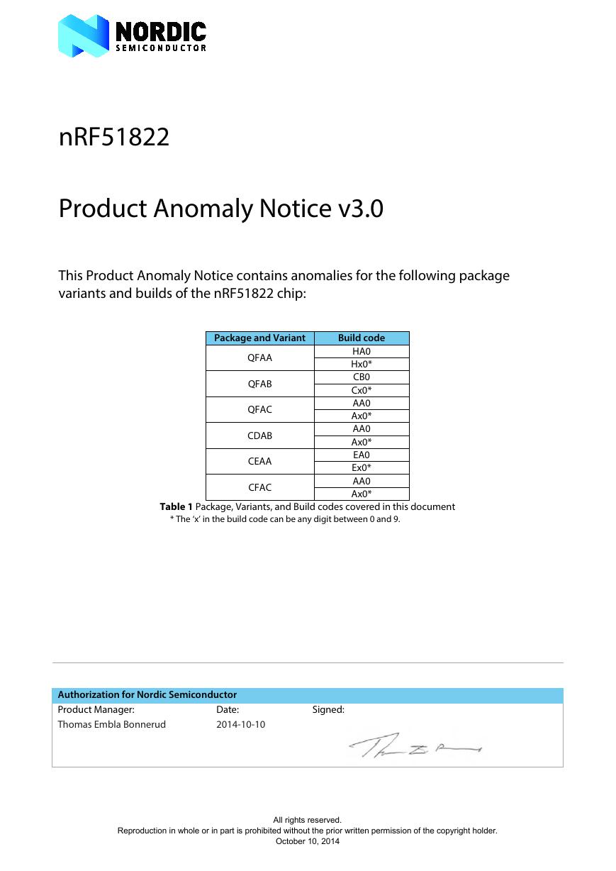
This Product Anomaly Notice contains anomalies for the following package
variants and builds of the nRF51822 chip:
Package and Variant
Build code
QFAA
QFAB
QFAC
CDAB
CEAA
CFAC
HA0
Hx0*
CB0
Cx0*
AA0
Ax0*
AA0
Ax0*
EA0
Ex0*
AA0
Ax0*
Table 1 Package, Variants, and Build codes covered in this document
* The ‘x’ in the build code can be any digit between 0 and 9.
Authorization for Nordic Semiconductor
Date:
Product Manager:
Thomas Embla Bonnerud
2014-10-10
Signed:
Reproduction in whole or in part is prohibited without the prior written permission of the copyright holder.
All rights reserved.
October 10, 2014
�
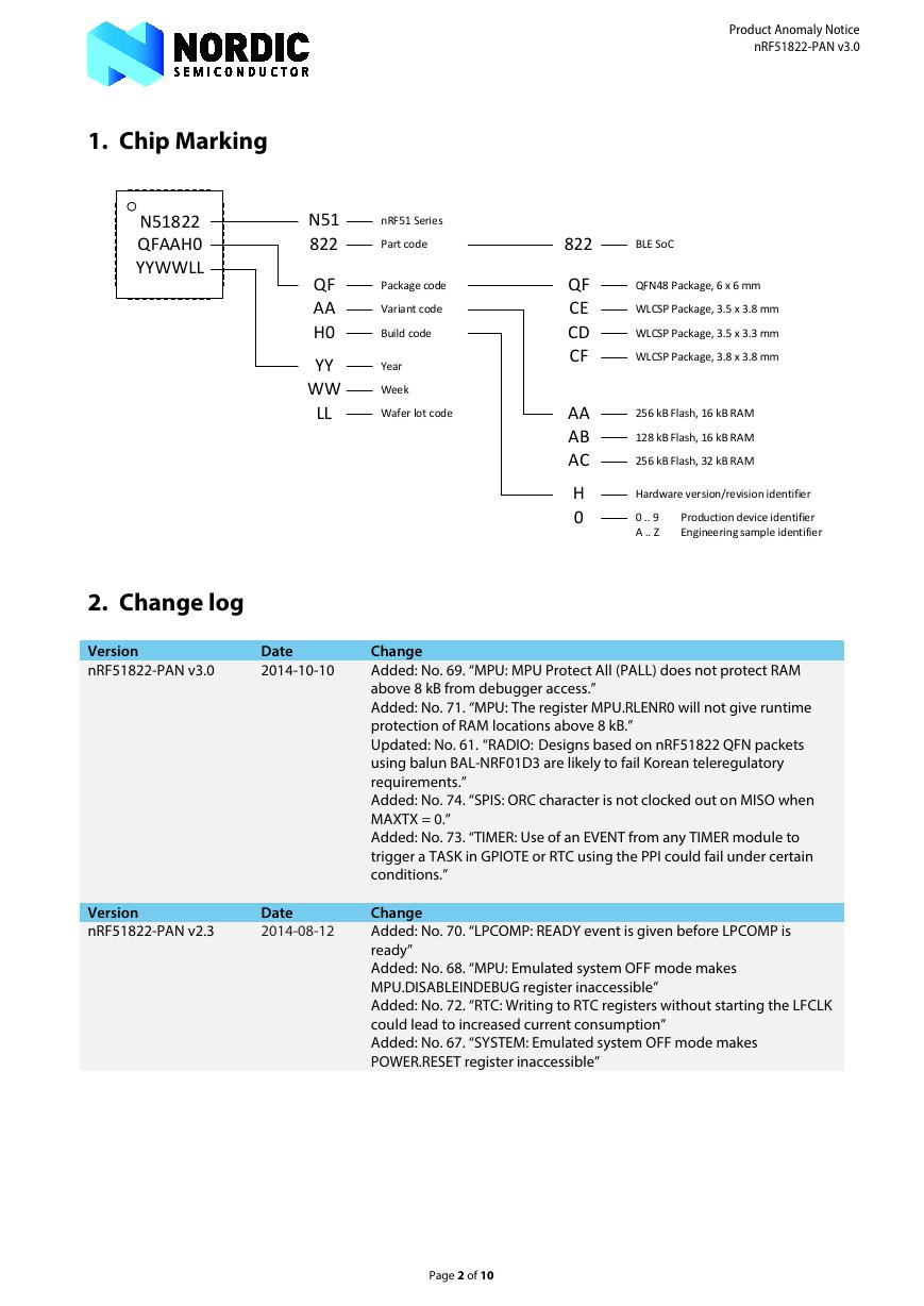
1. Chip Marking
N51822
QFAAH0
YYWWLL
N51
822
QF
AA
H0
YY
WW
LL
nRF51 Series
Part code
Package code
Variant code
Build code
Year
Week
Wafer lot code
Product Anomaly Notice
nRF51822-PAN v3.0
822
BLE SoC
QF
CE
CD
CF
AA
AB
AC
H
0
QFN48 Package, 6 x 6 mm
WLCSP Package, 3.5 x 3.8 mm
WLCSP Package, 3.5 x 3.3 mm
WLCSP Package, 3.8 x 3.8 mm
256 kB Flash, 16 kB RAM
128 kB Flash, 16 kB RAM
256 kB Flash, 32 kB RAM
Hardware version/revision identifier
0 .. 9
A .. Z
Production device identifier
Engineering sample identifier
2. Change log
Version
nRF51822-PAN v3.0
Date
2014-10-10
Version
nRF51822-PAN v2.3
Date
2014-08-12
Change
Added: No. 69. “MPU: MPU Protect All (PALL) does not protect RAM
above 8 kB from debugger access.”
Added: No. 71. “MPU: The register MPU.RLENR0 will not give runtime
protection of RAM locations above 8 kB.”
Updated: No. 61. “RADIO: Designs based on nRF51822 QFN packets
using balun BAL-NRF01D3 are likely to fail Korean teleregulatory
requirements.”
Added: No. 74. “SPIS: ORC character is not clocked out on MISO when
MAXTX = 0.”
Added: No. 73. “TIMER: Use of an EVENT from any TIMER module to
trigger a TASK in GPIOTE or RTC using the PPI could fail under certain
conditions.”
Change
Added: No. 70. “LPCOMP: READY event is given before LPCOMP is
ready”
Added: No. 68. “MPU: Emulated system OFF mode makes
MPU.DISABLEINDEBUG register inaccessible”
Added: No. 72. “RTC: Writing to RTC registers without starting the LFCLK
could lead to increased current consumption”
Added: No. 67. “SYSTEM: Emulated system OFF mode makes
POWER.RESET register inaccessible”
Page 2 of 10
�
Product Anomaly Notice
nRF51822-PAN v3.0
QFAA
QFAB
CDAB
CEAA
X
X
X
X
X
X
X
X
X
QFAC
CFAC
New/
Inherited1
X
Inherited
X
X
X
X
X
X
New
New
Inherited
Inherited
New and
inherited
Inherited
New
Inherited
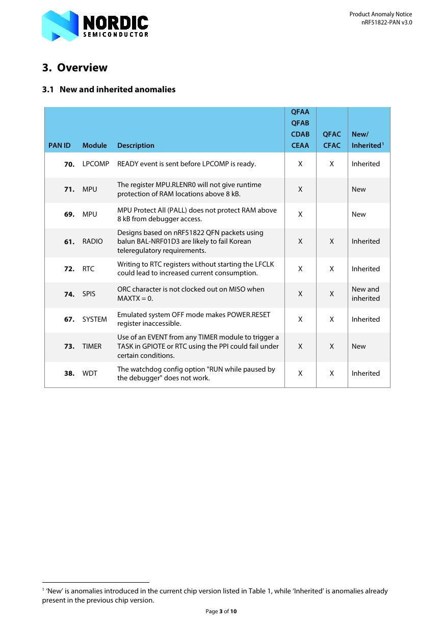
3. Overview
3.1 New and inherited anomalies
PAN ID Module Description
70. LPCOMP READY event is sent before LPCOMP is ready.
71. MPU
69. MPU
61. RADIO
72. RTC
74. SPIS
The register MPU.RLENR0 will not give runtime
protection of RAM locations above 8 kB.
MPU Protect All (PALL) does not protect RAM above
8 kB from debugger access.
Designs based on nRF51822 QFN packets using
balun BAL-NRF01D3 are likely to fail Korean
teleregulatory requirements.
Writing to RTC registers without starting the LFCLK
could lead to increased current consumption.
ORC character is not clocked out on MISO when
MAXTX = 0.
67. SYSTEM
Emulated system OFF mode makes POWER.RESET
register inaccessible.
73. TIMER
Use of an EVENT from any TIMER module to trigger a
TASK in GPIOTE or RTC using the PPI could fail under
certain conditions.
38. WDT
The watchdog config option "RUN while paused by
the debugger" does not work.
1 ‘New’ is anomalies introduced in the current chip version listed in Table 1, while ‘Inherited’ is anomalies already
present in the previous chip version.
Page 3 of 10
�
Product Anomaly Notice
nRF51822-PAN v3.0
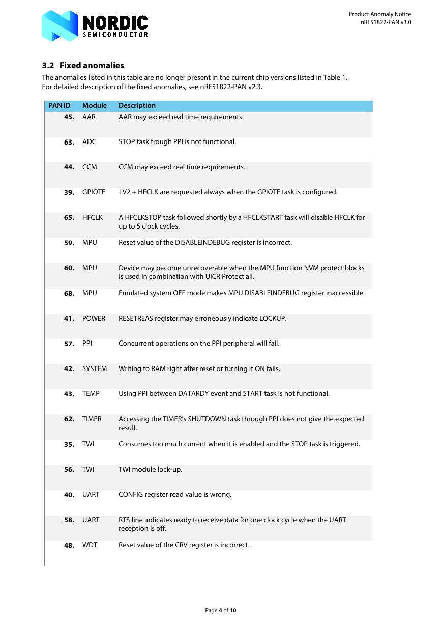
3.2 Fixed anomalies
The anomalies listed in this table are no longer present in the current chip versions listed in Table 1.
For detailed description of the fixed anomalies, see nRF51822-PAN v2.3.
Description
AAR may exceed real time requirements.
PAN ID Module
45. AAR
63. ADC
STOP task trough PPI is not functional.
44. CCM
CCM may exceed real time requirements.
39. GPIOTE
1V2 + HFCLK are requested always when the GPIOTE task is configured.
65. HFCLK
A HFCLKSTOP task followed shortly by a HFCLKSTART task will disable HFCLK for
up to 5 clock cycles.
59. MPU
Reset value of the DISABLEINDEBUG register is incorrect.
60. MPU
Device may become unrecoverable when the MPU function NVM protect blocks
is used in combination with UICR Protect all.
68. MPU
Emulated system OFF mode makes MPU.DISABLEINDEBUG register inaccessible.
41. POWER
RESETREAS register may erroneously indicate LOCKUP.
57. PPI
Concurrent operations on the PPI peripheral will fail.
42. SYSTEM Writing to RAM right after reset or turning it ON fails.
43. TEMP
Using PPI between DATARDY event and START task is not functional.
62. TIMER
Accessing the TIMER’s SHUTDOWN task through PPI does not give the expected
result.
35. TWI
Consumes too much current when it is enabled and the STOP task is triggered.
56. TWI
TWI module lock-up.
40. UART
CONFIG register read value is wrong.
58. UART
RTS line indicates ready to receive data for one clock cycle when the UART
reception is off.
48. WDT
Reset value of the CRV register is incorrect.
Page 4 of 10
�
4. New and inherited anomalies
Product Anomaly Notice
nRF51822-PAN v3.0
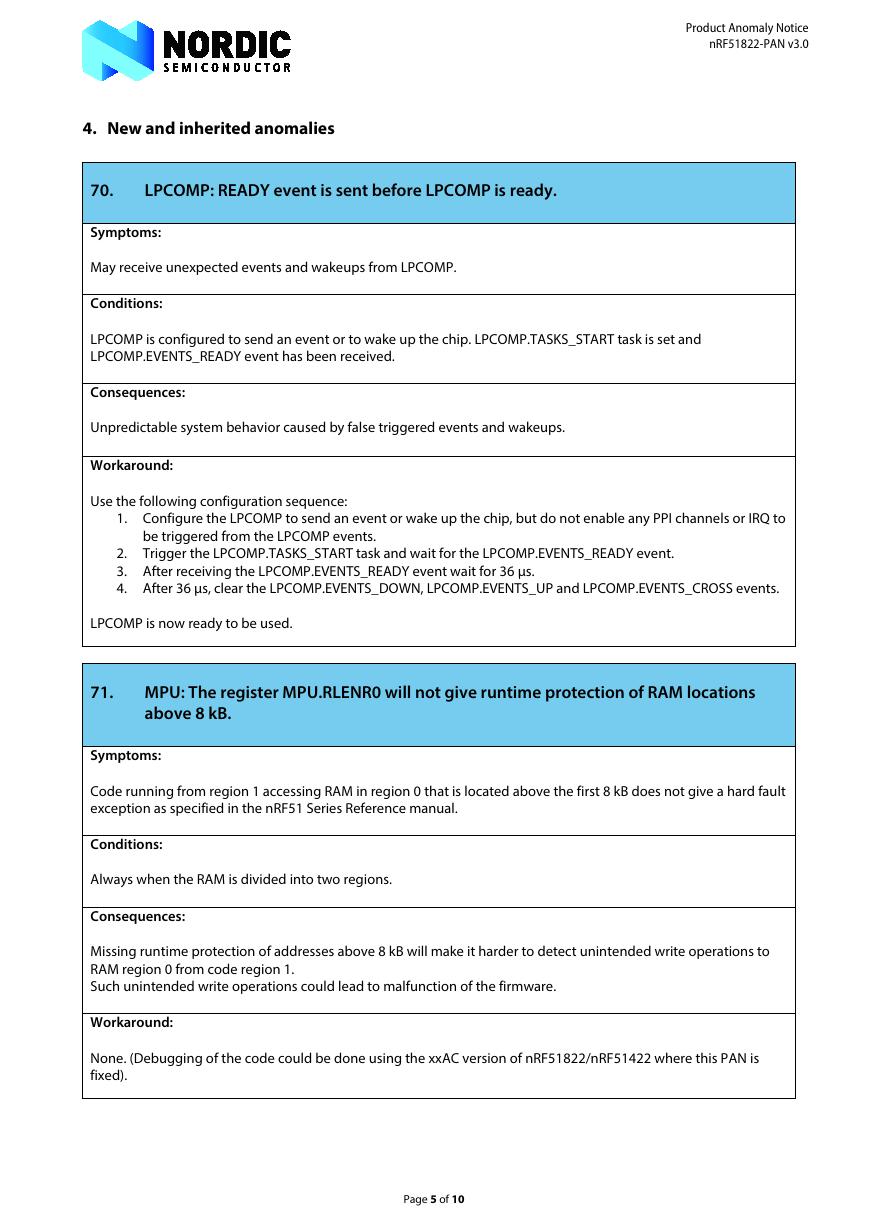
LPCOMP: READY event is sent before LPCOMP is ready.
70.
Symptoms:
May receive unexpected events and wakeups from LPCOMP.
Conditions:
LPCOMP is configured to send an event or to wake up the chip. LPCOMP.TASKS_START task is set and
LPCOMP.EVENTS_READY event has been received.
Consequences:
Unpredictable system behavior caused by false triggered events and wakeups.
Workaround:
Use the following configuration sequence:
1. Configure the LPCOMP to send an event or wake up the chip, but do not enable any PPI channels or IRQ to
be triggered from the LPCOMP events.
2. Trigger the LPCOMP.TASKS_START task and wait for the LPCOMP.EVENTS_READY event.
3. After receiving the LPCOMP.EVENTS_READY event wait for 36 µs.
4. After 36 µs, clear the LPCOMP.EVENTS_DOWN, LPCOMP.EVENTS_UP and LPCOMP.EVENTS_CROSS events.
LPCOMP is now ready to be used.
71. MPU: The register MPU.RLENR0 will not give runtime protection of RAM locations
above 8 kB.
Symptoms:
Code running from region 1 accessing RAM in region 0 that is located above the first 8 kB does not give a hard fault
exception as specified in the nRF51 Series Reference manual.
Conditions:
Always when the RAM is divided into two regions.
Consequences:
Missing runtime protection of addresses above 8 kB will make it harder to detect unintended write operations to
RAM region 0 from code region 1.
Such unintended write operations could lead to malfunction of the firmware.
Workaround:
None. (Debugging of the code could be done using the xxAC version of nRF51822/nRF51422 where this PAN is
fixed).
Page 5 of 10
�
Product Anomaly Notice
nRF51822-PAN v3.0
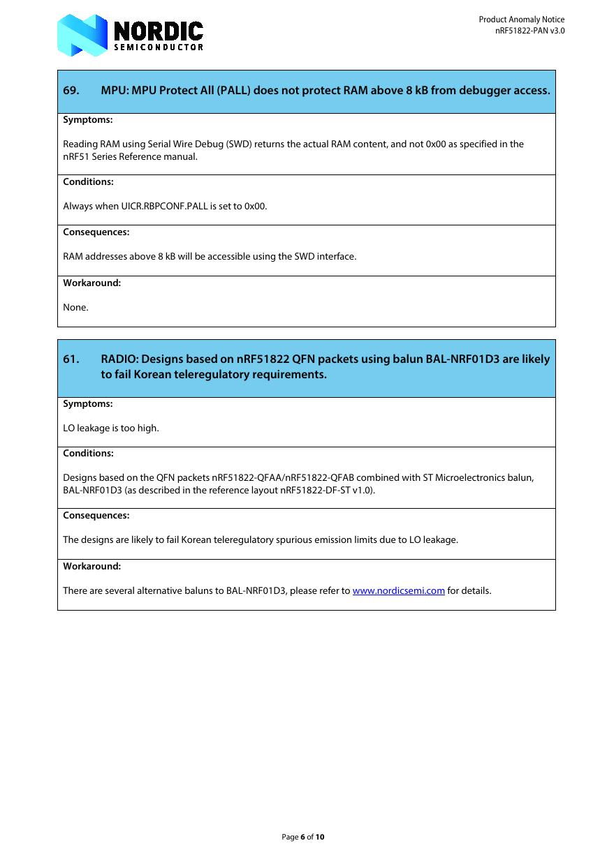
69. MPU: MPU Protect All (PALL) does not protect RAM above 8 kB from debugger access.
Symptoms:
Reading RAM using Serial Wire Debug (SWD) returns the actual RAM content, and not 0x00 as specified in the
nRF51 Series Reference manual.
Conditions:
Always when UICR.RBPCONF.PALL is set to 0x00.
Consequences:
RAM addresses above 8 kB will be accessible using the SWD interface.
Workaround:
None.
61.
RADIO: Designs based on nRF51822 QFN packets using balun BAL-NRF01D3 are likely
to fail Korean teleregulatory requirements.
Symptoms:
LO leakage is too high.
Conditions:
Designs based on the QFN packets nRF51822-QFAA/nRF51822-QFAB combined with ST Microelectronics balun,
BAL-NRF01D3 (as described in the reference layout nRF51822-DF-ST v1.0).
Consequences:
The designs are likely to fail Korean teleregulatory spurious emission limits due to LO leakage.
Workaround:
There are several alternative baluns to BAL-NRF01D3, please refer to www.nordicsemi.com for details.
Page 6 of 10
�
Product Anomaly Notice
nRF51822-PAN v3.0
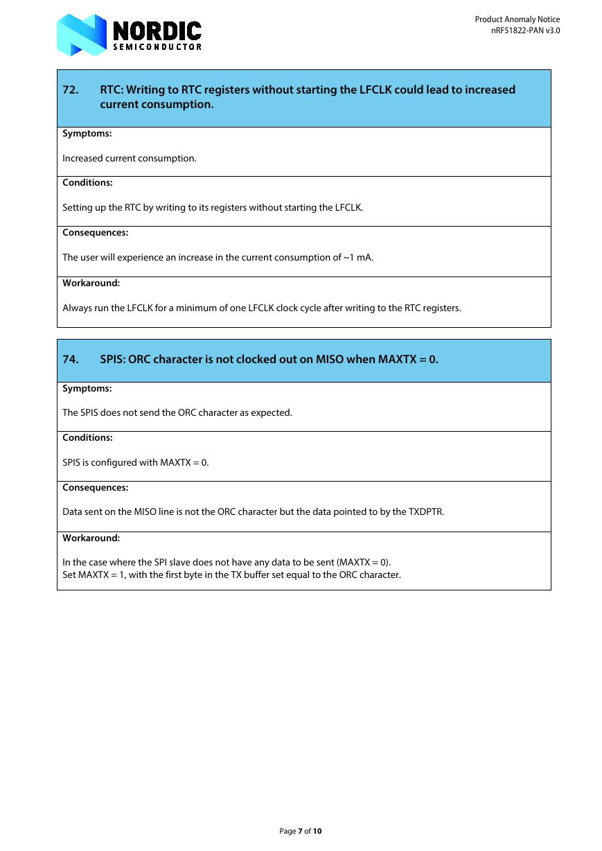
RTC: Writing to RTC registers without starting the LFCLK could lead to increased
current consumption.
72.
Symptoms:
Increased current consumption.
Conditions:
Setting up the RTC by writing to its registers without starting the LFCLK.
Consequences:
The user will experience an increase in the current consumption of ~1 mA.
Workaround:
Always run the LFCLK for a minimum of one LFCLK clock cycle after writing to the RTC registers.
SPIS: ORC character is not clocked out on MISO when MAXTX = 0.
74.
Symptoms:
The SPIS does not send the ORC character as expected.
Conditions:
SPIS is configured with MAXTX = 0.
Consequences:
Data sent on the MISO line is not the ORC character but the data pointed to by the TXDPTR.
Workaround:
In the case where the SPI slave does not have any data to be sent (MAXTX = 0).
Set MAXTX = 1, with the first byte in the TX buffer set equal to the ORC character.
Page 7 of 10
�
Product Anomaly Notice
nRF51822-PAN v3.0
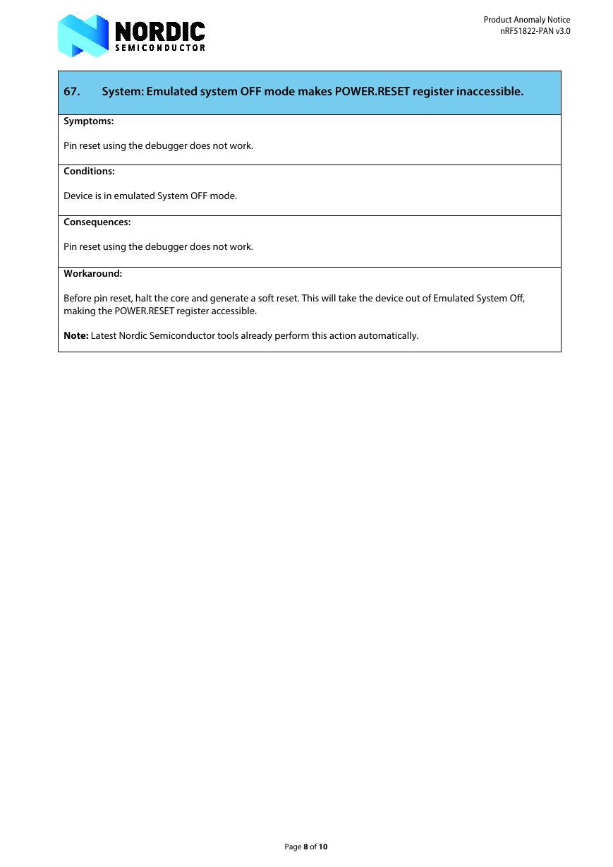
System: Emulated system OFF mode makes POWER.RESET register inaccessible.
67.
Symptoms:
Pin reset using the debugger does not work.
Conditions:
Device is in emulated System OFF mode.
Consequences:
Pin reset using the debugger does not work.
Workaround:
Before pin reset, halt the core and generate a soft reset. This will take the device out of Emulated System Off,
making the POWER.RESET register accessible.
Note: Latest Nordic Semiconductor tools already perform this action automatically.
Page 8 of 10
�


 V2版本原理图(Capacitive-Fingerprint-Reader-Schematic_V2).pdf
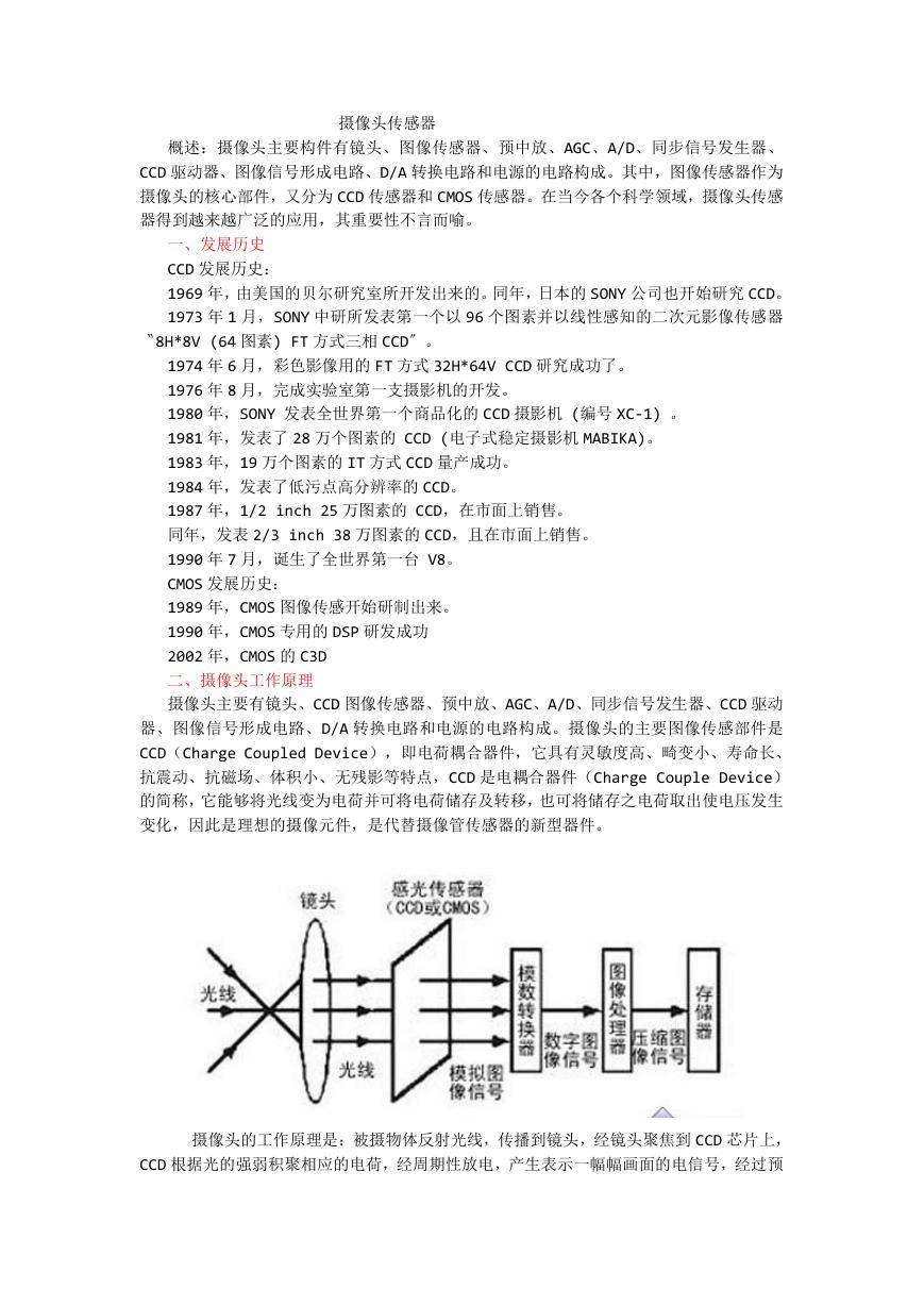 摄像头工作原理.doc
 VL53L0X简要说明(En.FLVL53L00216).pdf
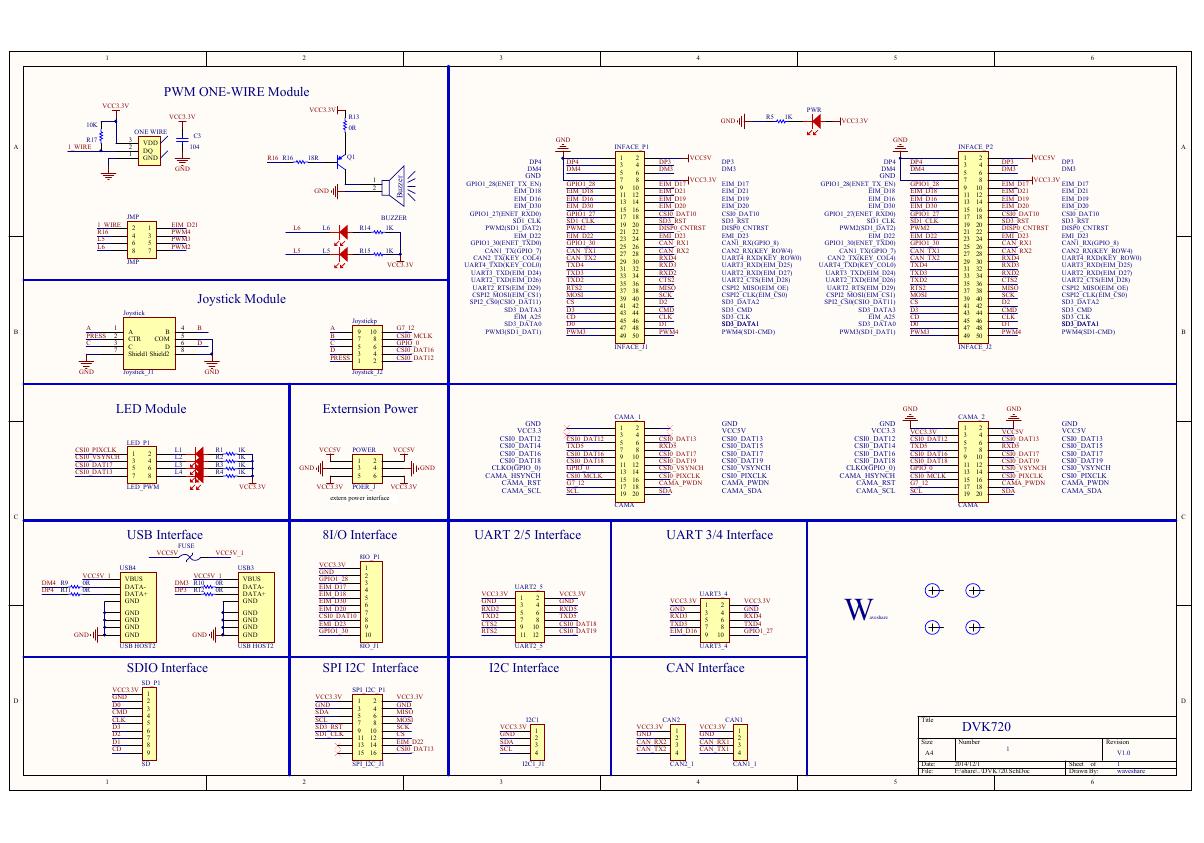 原理图(DVK720-Schematic).pdf
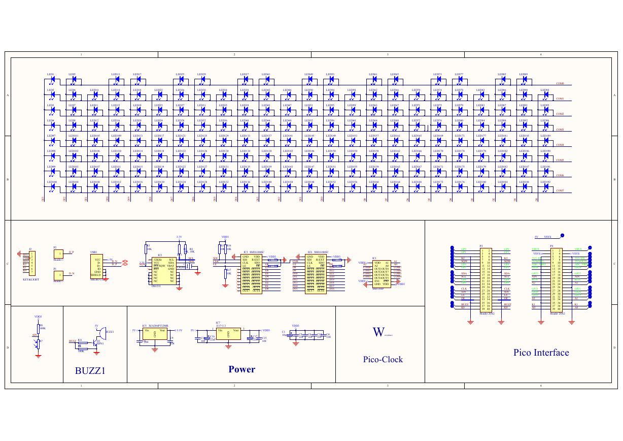 原理图(Pico-Clock-Green-Schdoc).pdf
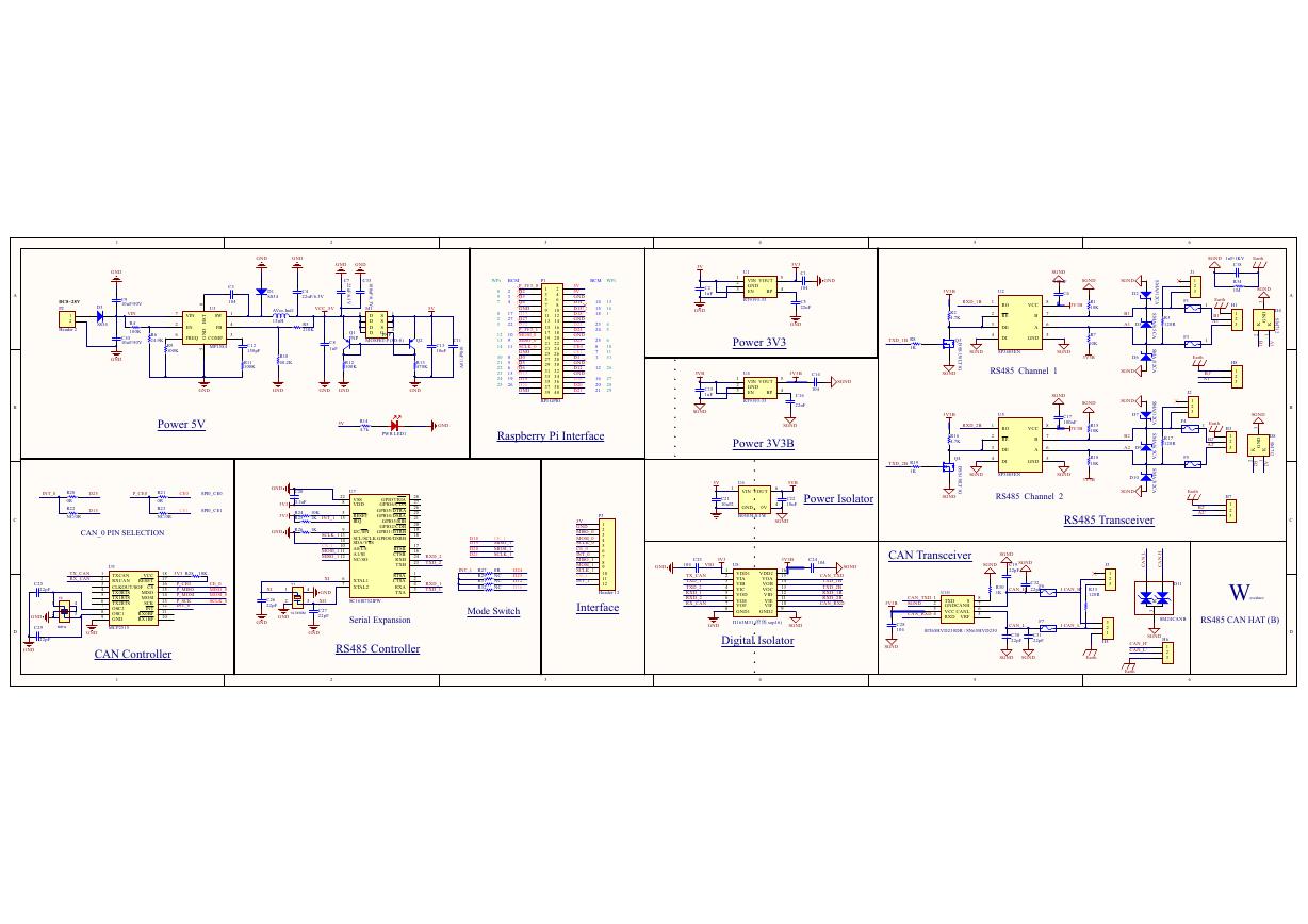 原理图(RS485-CAN-HAT-B-schematic).pdf
 File:SIM7500_SIM7600_SIM7800 Series_SSL_Application Note_V2.00.pdf
 ADS1263(Ads1262).pdf
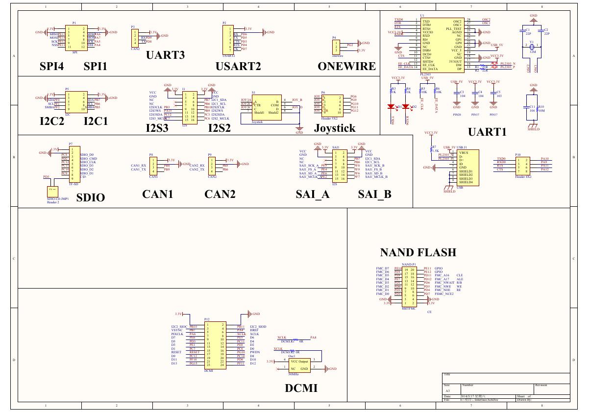 原理图(Open429Z-D-Schematic).pdf
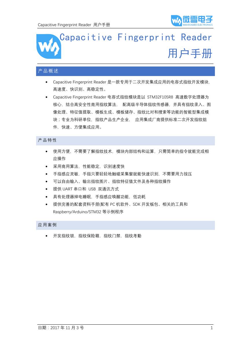 用户手册(Capacitive_Fingerprint_Reader_User_Manual_CN).pdf
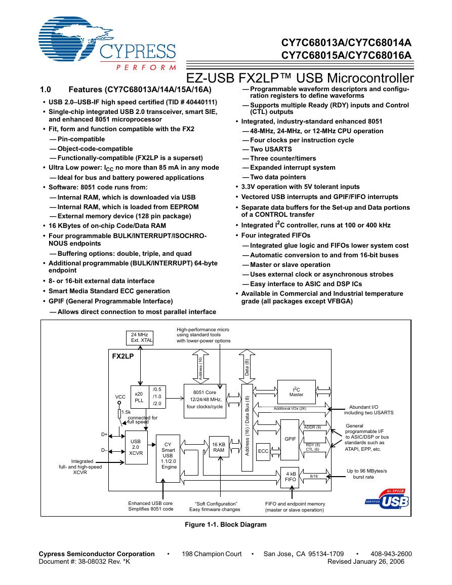 CY7C68013A(英文版)(CY7C68013A).pdf
 TechnicalReference_Dem.pdf