General Description
TSL2580, TSL2581
Light-to-Digital Converter
The TSL2580 and TSL2581 are very-high sensitivity
light-to-digital converters that transform light intensity to a
digital signal output capable of direct I²C (TSL2581) or SMBus
(TSL2580) interface. Each device combines one broadband
photodiode (visible plus infrared) and one infrared-responding
photodiode on a single CMOS integrated circuit capable of
providing a near-photopic response over an effective 16-bit
dynamic range (16-bit resolution). Two integrating ADCs
convert the photodiode currents to a digital output that
represents the irradiance measured on each channel. This
digital output can be input to a microprocessor where
illuminance (ambient light level) in lux is derived using an
empirical formula to approximate the human eye response. The
TSL2580 device permits an SMB-Alert style interrupt, and the
TSL2581 device supports a traditional level style interrupt that
remains asserted until the firmware clears it.
While useful for general purpose light sensing applications, the
TSL2580/81 devices are designed particularly for display panels
(LCD, OLED, etc.) with the purpose of extending battery life and
providing optimum viewing in diverse lighting conditions.
Display panel backlighting, which can account for up to 30 to
40 percent of total platform power, can be automatically
managed. Both devices are also ideal for controlling keyboard
illumination based upon ambient lighting conditions.
Illuminance information can further be used to manage
exposure control in digital cameras. The TSL2580/81 devices are
ideal in notebook/tablet PCs, LCD monitors, flat-panel
televisions, cell phones, and digital cameras. In addition, other
applications include street light control, security lighting,
sunlight harvesting, machine vision, and automotive
instrumentation clusters.
Ordering Information and Content Guide appear at end of
datasheet.
ams Datasheet
[v1-00] 2016-Apr-05
Page 1
Document Feedback
�
TSL2580, TSL2581 − General Description
Key Benefits & Features
The benefits and features of TSL2580, TSL2581, Light-to-Digital
Converter are listed below:
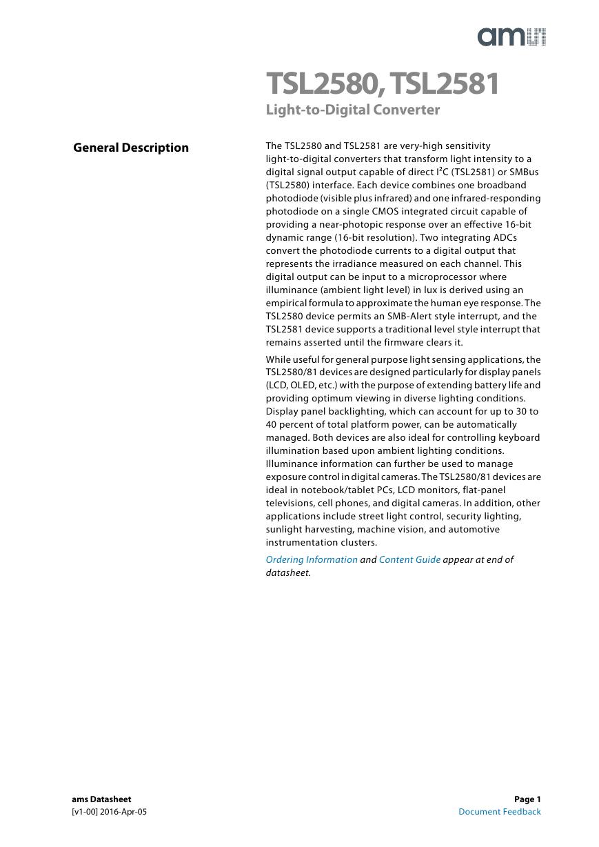
Figure 1:
Added Value Of Using TSL2580, TSL2581
Benefits
Features
• Enables Operation in IR Light Environments
• Patented Dual-Diode Architecture
• Enables Dark Room to High Lux Sunlight
Operation
• 1M:1 Dynamic Range
• Digital Interface is Less Susceptible to Noise
• SMBus Digital Interface
• Enables Low Standby Power Consumption
• 3μA Quiescent Current
• Reduces Board Space Requirements while
• Available in 1.25mm x 1.75mm Chipscale or 2mm x 2mm
Simplifying Designs
Dual Flat No-Lead (FN) Packages
• Approximately 30x More Sensitive Than the TSL2560/61
Device
• Approximates Human Eye Response
• Programmable ALS Interrupt Function with User-Defined
Upper and Lower Threshold Settings
• 16-Bit Digital Output with SMBus (TSL2580) at 100 kHz or
I²C (TSL2581) Fast-Mode at 400 kHz
• Programmable Analog Gain and Integration Time
Supporting 1,000,000-to-1 Dynamic Range
• Automatically Rejects 50/60-Hz Lighting Ripple
Applications
TSL2580, TSL2581, Light-to-Digital Converter is ideal for:
• Ambient Light Sensor (ALS) for Smart Phones, Digital
Photo Frames, and Portable Navigation Systems
• ALS for LED Signs, Laptop Computers, and LCD TVs
Page 2
Document Feedback
ams Datasheet
[v1-00] 2016-Apr-05
�
TSL2580, TSL2581 − General Description
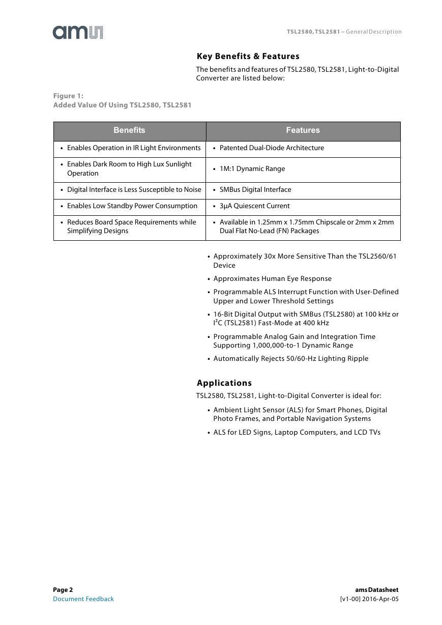
Figure 2:
TSL2580, TSL2581 Block Diagram
Block Diagram
The functional blocks of this device are shown below:
Channel 0
Visible and IR
Channel 1
IR Only
Integrating
A/D Converter
VDD = 2.7 V to 3.6 V
ADDR SEL
Address Select
Command
Register
ADC
Register
Interrupt
Two-Wire Serial Interface
INT
SCL
SDA
ams Datasheet
[v1-00] 2016-Apr-05
Page 3
Document Feedback
�
Pin Assignments
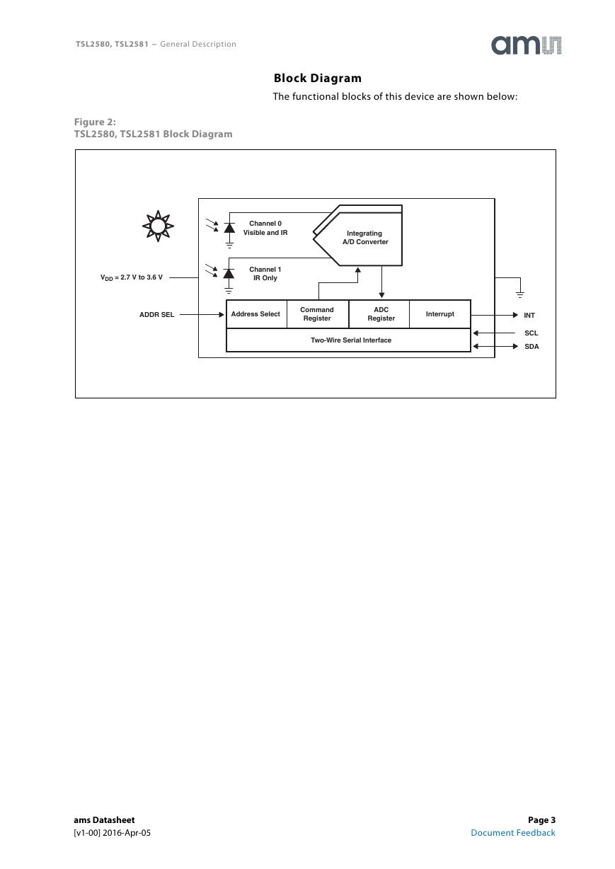
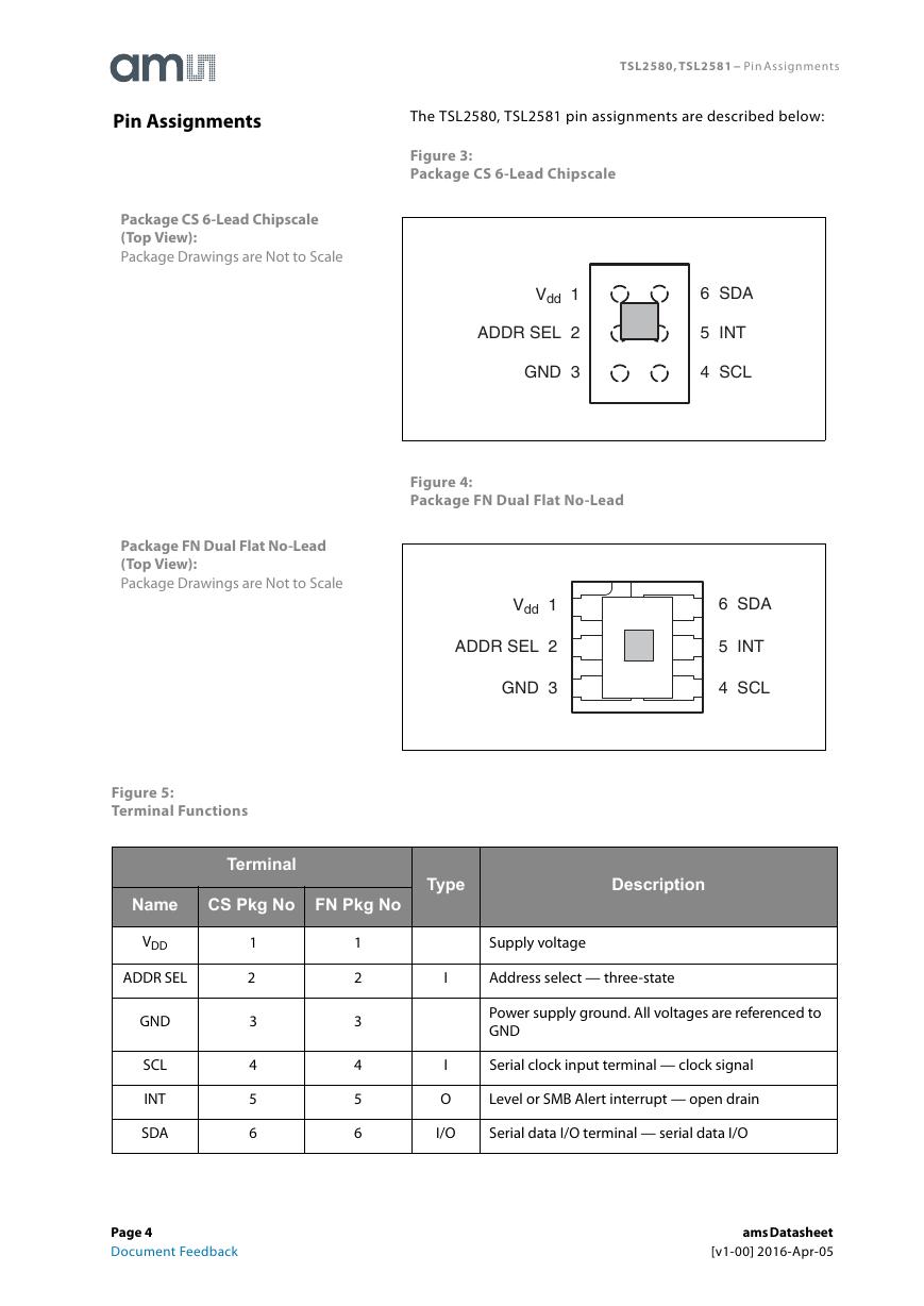
The TSL2580, TSL2581 pin assignments are described below:
Figure 3:
Package CS 6-Lead Chipscale
TSL2580, TSL2581 − Pin Assignments
Package CS 6-Lead Chipscale
(Top View):
Package Drawings are Not to Scale
Vdd 1
ADDR SEL 2
GND 3
6 SDA
5 INT
4 SCL
Figure 4:
Package FN Dual Flat No-Lead
Package FN Dual Flat No-Lead
(Top View):
Package Drawings are Not to Scale
Vdd 1
ADDR SEL 2
GND 3
6 SDA
5 INT
4 SCL
Figure 5:
Terminal Functions
Terminal
Name
CS Pkg No FN Pkg No
Type
Description
VDD
ADDR SEL
GND
SCL
INT
SDA
1
2
3
4
5
6
Page 4
Document Feedback
1
2
3
4
5
6
Supply voltage
I
Address select — three-state
Power supply ground. All voltages are referenced to
GND
I
O
Serial clock input terminal — clock signal
Level or SMB Alert interrupt — open drain
I/O
Serial data I/O terminal — serial data I/O
ams Datasheet
[v1-00] 2016-Apr-05
�
TSL2580, TSL2581 − Pin Assignments
Detailed Description
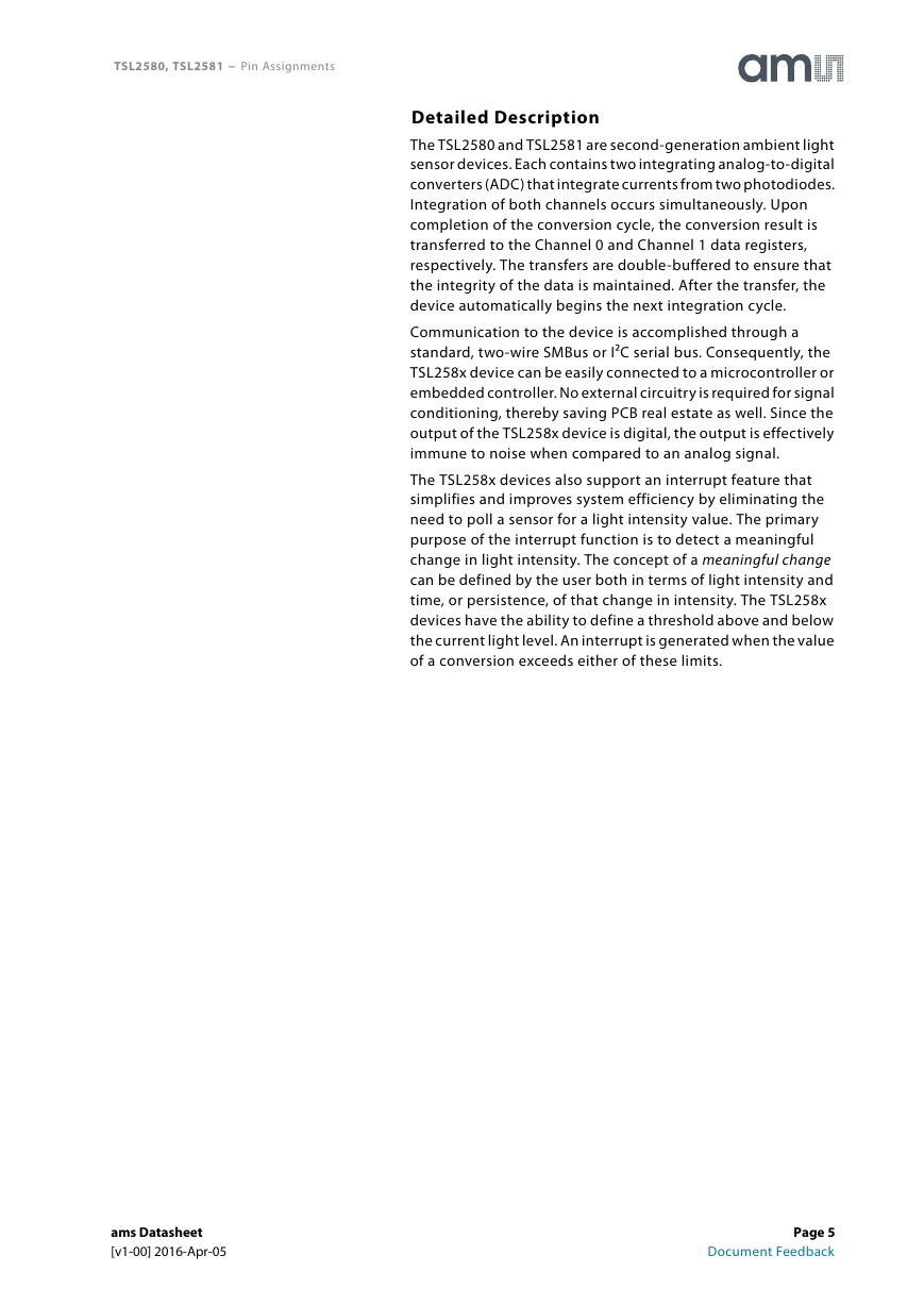
The TSL2580 and TSL2581 are second-generation ambient light
sensor devices. Each contains two integrating analog-to-digital
converters (ADC) that integrate currents from two photodiodes.
Integration of both channels occurs simultaneously. Upon
completion of the conversion cycle, the conversion result is
transferred to the Channel 0 and Channel 1 data registers,
respectively. The transfers are double-buffered to ensure that
the integrity of the data is maintained. After the transfer, the
device automatically begins the next integration cycle.
Communication to the device is accomplished through a
standard, two-wire SMBus or I²C serial bus. Consequently, the
TSL258x device can be easily connected to a microcontroller or
embedded controller. No external circuitry is required for signal
conditioning, thereby saving PCB real estate as well. Since the
output of the TSL258x device is digital, the output is effectively
immune to noise when compared to an analog signal.
The TSL258x devices also support an interrupt feature that
simplifies and improves system efficiency by eliminating the
need to poll a sensor for a light intensity value. The primary
purpose of the interrupt function is to detect a meaningful
change in light intensity. The concept of a meaningful change
can be defined by the user both in terms of light intensity and
time, or persistence, of that change in intensity. The TSL258x
devices have the ability to define a threshold above and below
the current light level. An interrupt is generated when the value
of a conversion exceeds either of these limits.
ams Datasheet
[v1-00] 2016-Apr-05
Page 5
Document Feedback
�
Absolute Maximum Ratings
TSL2580, TSL2581 − Absolute Maximum Ratings
Stresses beyond those listed under Absolute Maximum Ratings
may cause permanent damage to the device. These are stress
ratings only, and functional operation of the device at these or
any other conditions beyond those indicated under
Recommended Operating Conditions is not implied. Exposure
to absolute-maximum-rated conditions for extended periods
may affect device reliability.
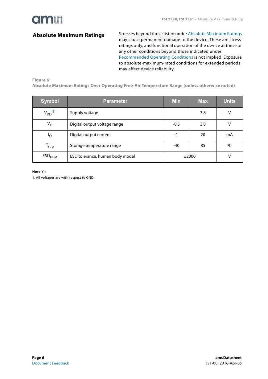
Figure 6:
Absolute Maximum Ratings Over Operating Free-Air Temperature Range (unless otherwise noted)
Symbol
Parameter
Min
Max
Units
VDD
(1)
Supply voltage
VO
IO
Tstrg
Digital output voltage range
Digital output current
Storage temperature range
-0.5
-1
-40
3.8
3.8
20
85
ESDHBM
ESD tolerance, human body model
±2000
V
V
mA
ºC
V
Note(s):
1. All voltages are with respect to GND.
Page 6
Document Feedback
ams Datasheet
[v1-00] 2016-Apr-05
�
TSL2580, TSL2581 − Electrical Characteristics
Electrical Characteristics
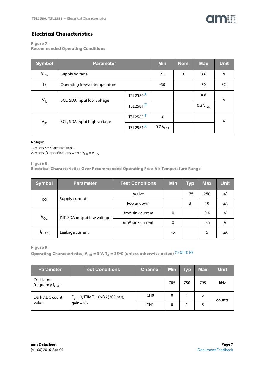
Figure 7:
Recommended Operating Conditions
Symbol
Parameter
Min
Nom
Max
Unit
VDD
TA
VIL
VIH
Supply voltage
Operating free-air temperature
SCL, SDA input low voltage
SCL, SDA input high voltage
3
2.7
-30
TSL2580(1)
TSL2581(2)
TSL2580(1)
2
TSL2581(2)
0.7 VDD
3.6
70
0.8
0.3 VDD
V
ºC
V
V
Note(s):
1. Meets SMB specifications.
2. Meets I²C specifications where VDD = VBUS.
Figure 8:
Electrical Characteristics Over Recommended Operating Free-Air Temperature Range
Symbol
Parameter
Test Conditions
Min
IDD
Supply current
VOL
ILEAK
INT, SDA output low voltage
Leakage current
Active
Power down
3mA sink current
6mA sink current
0
0
-5
Typ
175
3
Max
250
10
0.4
0.6
5
Unit
μA
μA
V
V
μA
Figure 9:
Operating Characteristics; VDD = 3 V, TA = 25ºC (unless otherwise noted) (1) (2) (3) (4)
Parameter
Test Conditions
Channel
Min
Typ Max
Unit
Oscillator
frequency fOSC
705
750
795
kHz
Dark ADC count
value
Ee = 0, ITIME = 0xB6 (200 ms),
gain=16x
CH0
CH1
0
0
1
1
5
5
counts
ams Datasheet
[v1-00] 2016-Apr-05
Page 7
Document Feedback
�
Parameter
Test Conditions
Channel
Min
Typ Max
Unit
TSL2580, TSL2581 − Electrical Characteristics
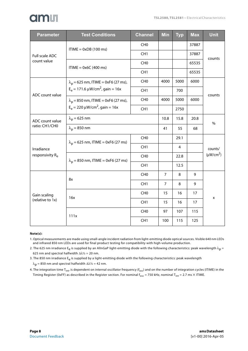
Full scale ADC
count value
ITIME = 0xDB (100 ms)
ITIME = 0x6C (400 ms)
ADC count value
ADC count value
ratio: CH1/CH0
Irradiance
responsivity Re
Gain scaling
(relative to 1x)
λp = 625 nm, ITIME = 0xF6 (27 ms),
Ee = 171.6 μW/cm2, gain = 16x
λp = 850 nm, ITIME = 0xF6 (27 ms),
Ee = 220 μW/cm2, gain = 16x
λp = 625 nm
λp = 850 nm
λp = 625 nm, ITIME = 0xF6 (27 ms)
λp = 850 nm, ITIME = 0xF6 (27 ms)
8x
16x
111x
CH0
CH1
CH0
CH1
CH0
CH1
CH0
CH1
CH0
CH1
CH0
CH1
CH0
CH1
CH0
CH1
CH0
CH1
37887
37887
65535
65535
4000
5000
6000
700
4000
5000
6000
2750
10.8
15.8
20.8
41
7
7
15
15
97
100
55
29.1
4
22.8
12.5
8
8
16
16
107
115
68
9
9
17
17
115
125
counts
counts
%
counts/
(μW/cm2)
x
Note(s):
1. Optical measurements are made using small-angle incident radiation from light-emitting diode optical sources. Visible 640 nm LEDs
and infrared 850 nm LEDs are used for final product testing for compatibility with high-volume production.
2. The 625 nm irradiance Ee is supplied by an AlInGaP light-emitting diode with the following characteristics: peak wavelength λp =
625 nm and spectral halfwidth Δλ½ = 20 nm.
3. The 850 nm irradiance Ee is supplied by a light-emitting diode with the following characteristics: peak wavelength
λp = 850 nm and spectral halfwidth Δλ½ = 42 nm.
4. The integration time Tint, is dependent on internal oscillator frequency (fosc) and on the number of integration cycles (ITIME) in the
Timing Register (0xFF) as described in the Register section. For nominal fosc = 750 kHz, nominal Tint = 2.7 ms × ITIME.
Page 8
Document Feedback
ams Datasheet
[v1-00] 2016-Apr-05
�


 V2版本原理图(Capacitive-Fingerprint-Reader-Schematic_V2).pdf
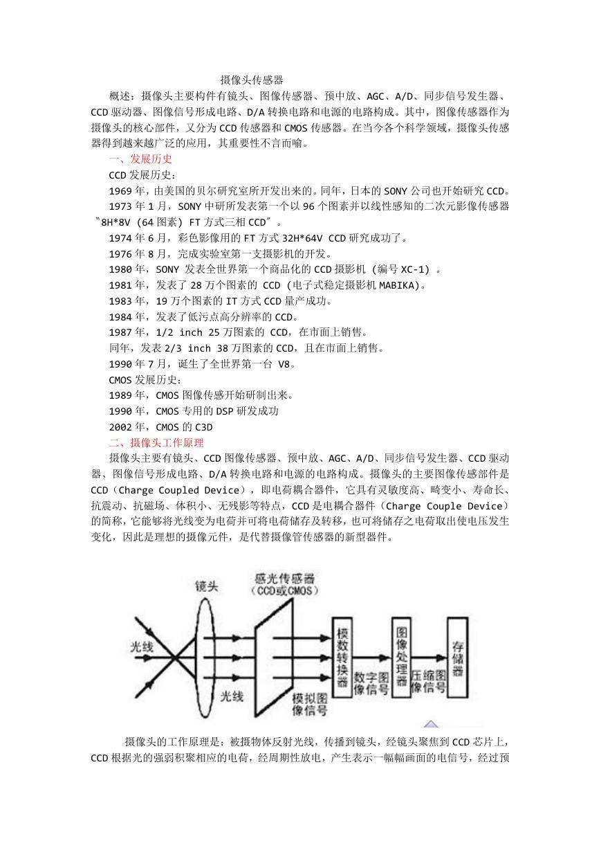 摄像头工作原理.doc
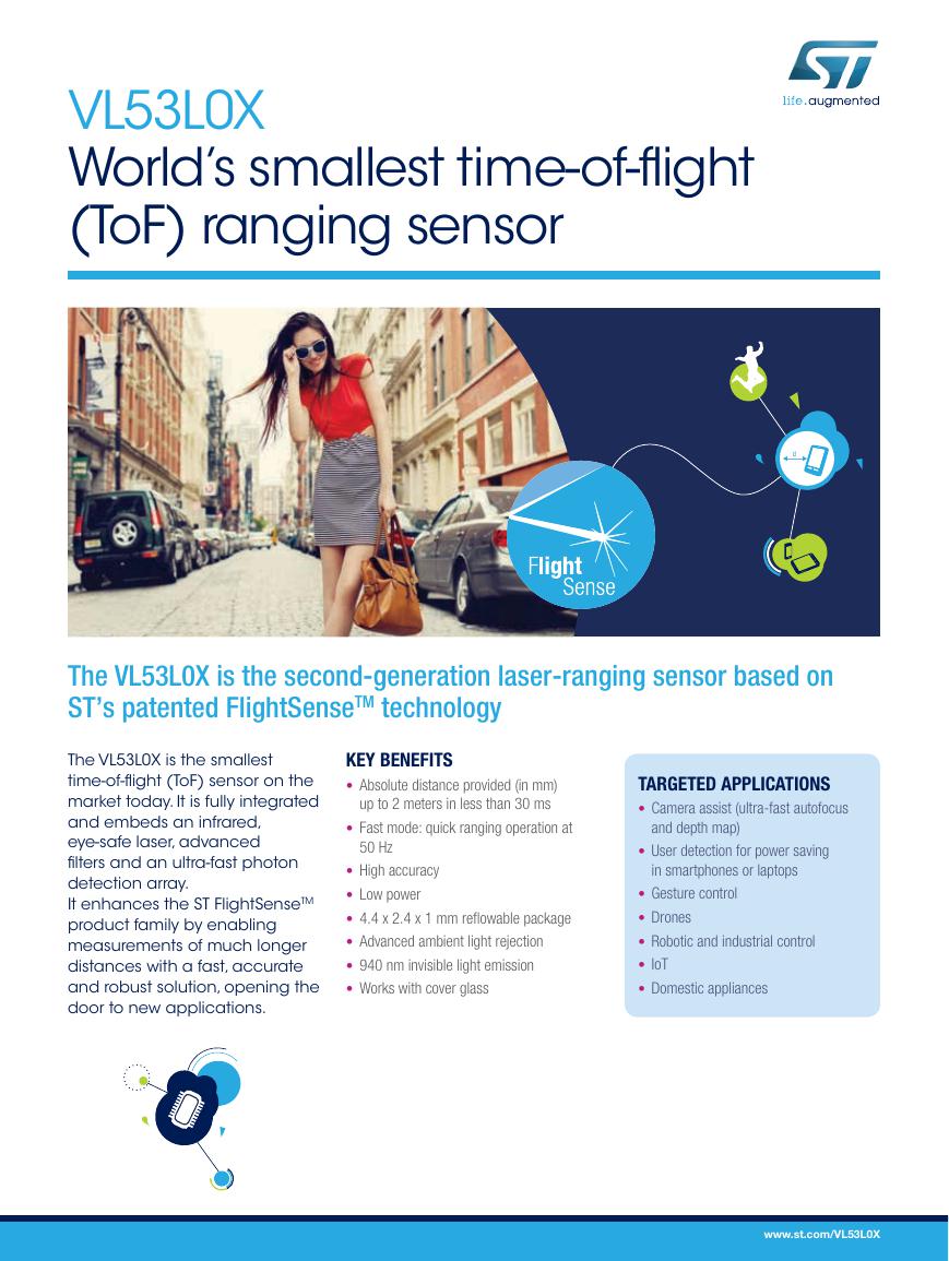 VL53L0X简要说明(En.FLVL53L00216).pdf
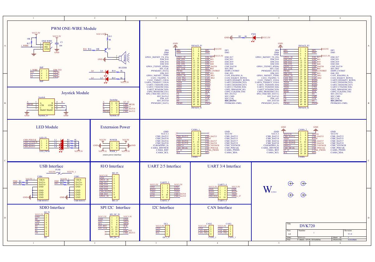 原理图(DVK720-Schematic).pdf
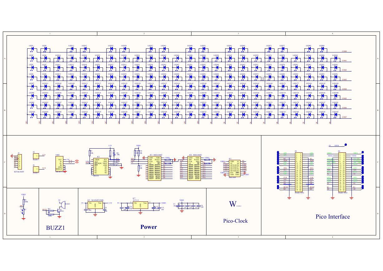 原理图(Pico-Clock-Green-Schdoc).pdf
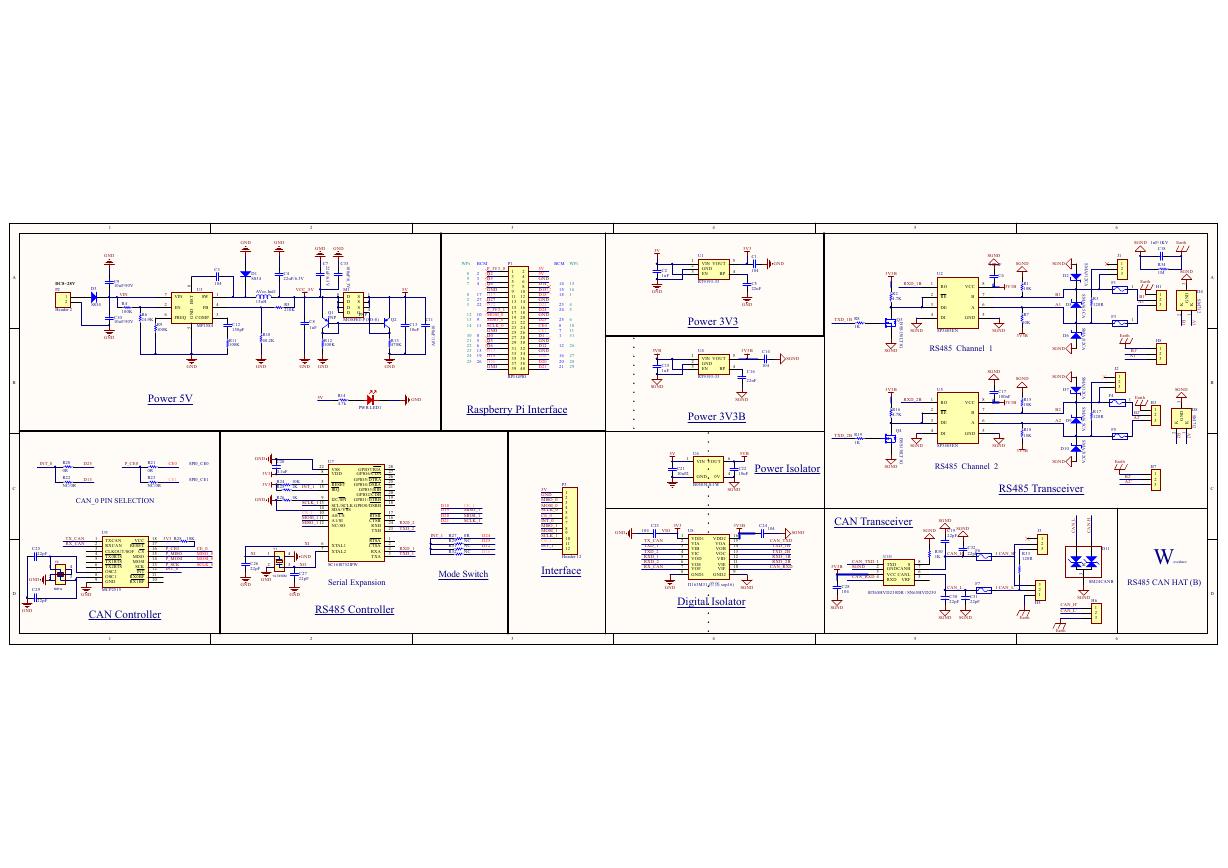 原理图(RS485-CAN-HAT-B-schematic).pdf
 File:SIM7500_SIM7600_SIM7800 Series_SSL_Application Note_V2.00.pdf
 ADS1263(Ads1262).pdf
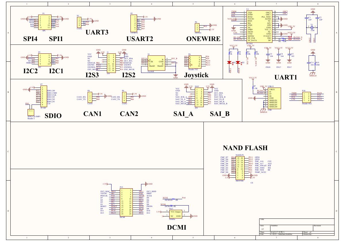 原理图(Open429Z-D-Schematic).pdf
 用户手册(Capacitive_Fingerprint_Reader_User_Manual_CN).pdf
 CY7C68013A(英文版)(CY7C68013A).pdf
 TechnicalReference_Dem.pdf