Application Note for FT5426-5526 CTPM
Application Note for FT5426 - 5526
CTPM
Application Note for FT5426 - 5526CTPM
Project name
Touch panel
Document ref
Version
Release date
Owner
Classification
Distribution List
Approval
[Document ref]
0.1
2015.9.06
B.F.Lu
This document contains information proprietary to FocalTech Systems, Ltd., and may
not be reproduced, disclosed or used in whole or part without the express written
permission of FocalTech Systems, Ltd.
Copyright © 2015, FocalTech Systems, Ltd
All rights reserved
3/F,Kingdom Sci-Tech Building,
5th Gaoxinnan Avenue, Hi-Tech Park,
Nanshan District ,Shenzhen, Gungdong, P.R. China
ZIP :518057
T +86 755 26588222
F +86 755 26712499
E support@focaltech-systems.com
www.focaltech-systems.com
THIS DOCUMENT CONTAINS INFORMATION PROPRIETARY TO FOCALTECH SYSTEMS, LTD., AND MAY NOT BE
REPRODUCED, DISCLOSED OR USED IN W HOLE OR PART W ITHOUT WRITTEN PERMISSION OF FOCALTECH SYSTEMS,
LTD.
�
Application Note for FT5426-5526 CTPM
Author
Lu bingfeng
Approved by
THIS DOCUMENT CONTAINS INFORMATION PROPRIETARY TO FOCALTECH SYSTEMS, LTD., AND MAY NOT BE
REPRODUCED, DISCLOSED OR USED IN W HOLE OR PART W ITHOUT WRITTEN PERMISSION OF FOCALTECH SYSTEMS,
LTD.
Revision History
Date
Version
List of changes
2015.09.06
0.1
Initial draft.
�
Application Note for FT5426-5526 CTPM
目录
1
1.1
CTPM interface to Host ............................................................................................................................................. 1
I2C Read/Write Interface description .................................................................................................................... 1
1.1.1 Host write data to slave .................................................................................................................................... 1
1.1.2 Host read data from slave ................................................................................................................................ 2
Interrupt signal from CTPM to Host ...................................................................................................................... 2
Reset signal from Host to CTPM........................................................................................................................... 3
Standard Application Circuit ...................................................................................................................................... 1
FT5426DQ8 typical application schematic............................................................................................................. 1
FT5526EEZ typical application schematic ............................................................................................................ 2
CTPM Register Mapping .......................................................................................................................................... 1
Working Mode ..................................................................................................................................................... 1
DEVICE_MODE.................................................................................................................................................. 3
GEST_ID ............................................................................................................................................................. 3
TD_STATUS ....................................................................................................................................................... 3
Pn_XH (n:1-5) ...................................................................................................................................................... 3
Pn_XL (n:1-5) ...................................................................................................................................................... 3
Pn_YH (n:1-5) ...................................................................................................................................................... 4
Pn_YL (n:1-2) ...................................................................................................................................................... 4
Pn_WEIGHT (n:1-5) ............................................................................................................................................ 4
Pn_MISC (n:1-5) .................................................................................................................................................. 5
Communication between host and CTPM .................................................................................................................. 5
Communication Contents ...................................................................................................................................... 5
I2C Example Code ............................................................................................................................................... 5
1.2
1.3
2
2.1
2.2
3
3.1
3.2
3.3
3.4
3.5
3.6
3.7
3.8
3.9
3.10
4
4.1
4.2
Terminology
CTP – Capacitive touch panel
CTPM – Capacitive touch panel module
TX – Transmitter
RX – Receiver
THIS DOCUMENT CONTAINS INFORMATION PROPRIETARY TO FOCALTECH SYSTEMS, LTD., AND MAY NOT BE
REPRODUCED, DISCLOSED OR USED IN W HOLE OR PART W ITHOUT WRITTEN PERMISSION OF FOCALTECH SYSTEMS,
LTD.
�
Application Note for FT5426-5526 CTPM
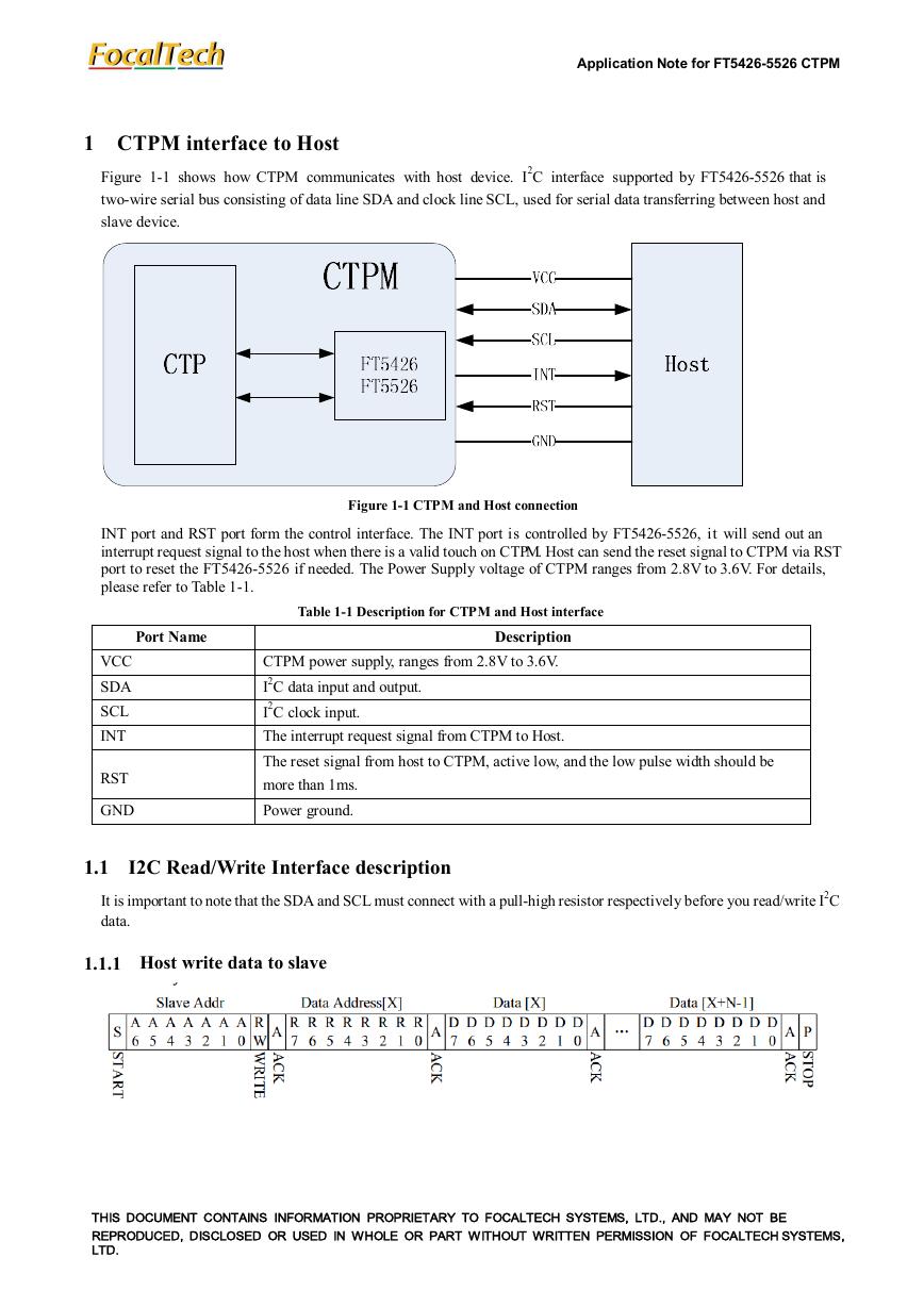
1 CTPM interface to Host
Figure 1-1 shows how CTPM communicates with host device. I2C interface supported by FT5426-5526 that is
two-wire serial bus consisting of data line SDA and clock line SCL, used for serial data transferring between host and
slave device.
Figure 1-1 CTPM and Host connection
INT port and RST port form the control interface. The INT port is controlled by FT5426-5526, it will send out an
interrupt request signal to the host when there is a valid touch on CTPM. Host can send the reset signal to CTPM via RST
port to reset the FT5426-5526 if needed. The Power Supply voltage of CTPM ranges from 2.8V to 3.6V. For details,
please refer to Table 1-1.
Port Name
VCC
SDA
SCL
INT
RST
GND
Table 1-1 Description for CTPM and Host interface
Description
CTPM power supply, ranges from 2.8V to 3.6V.
I2C data input and output.
I2C clock input.
The interrupt request signal from CTPM to Host.
The reset signal from host to CTPM, active low, and the low pulse width should be
more than 1ms.
Power ground.
1.1 I2C Read/Write Interface description
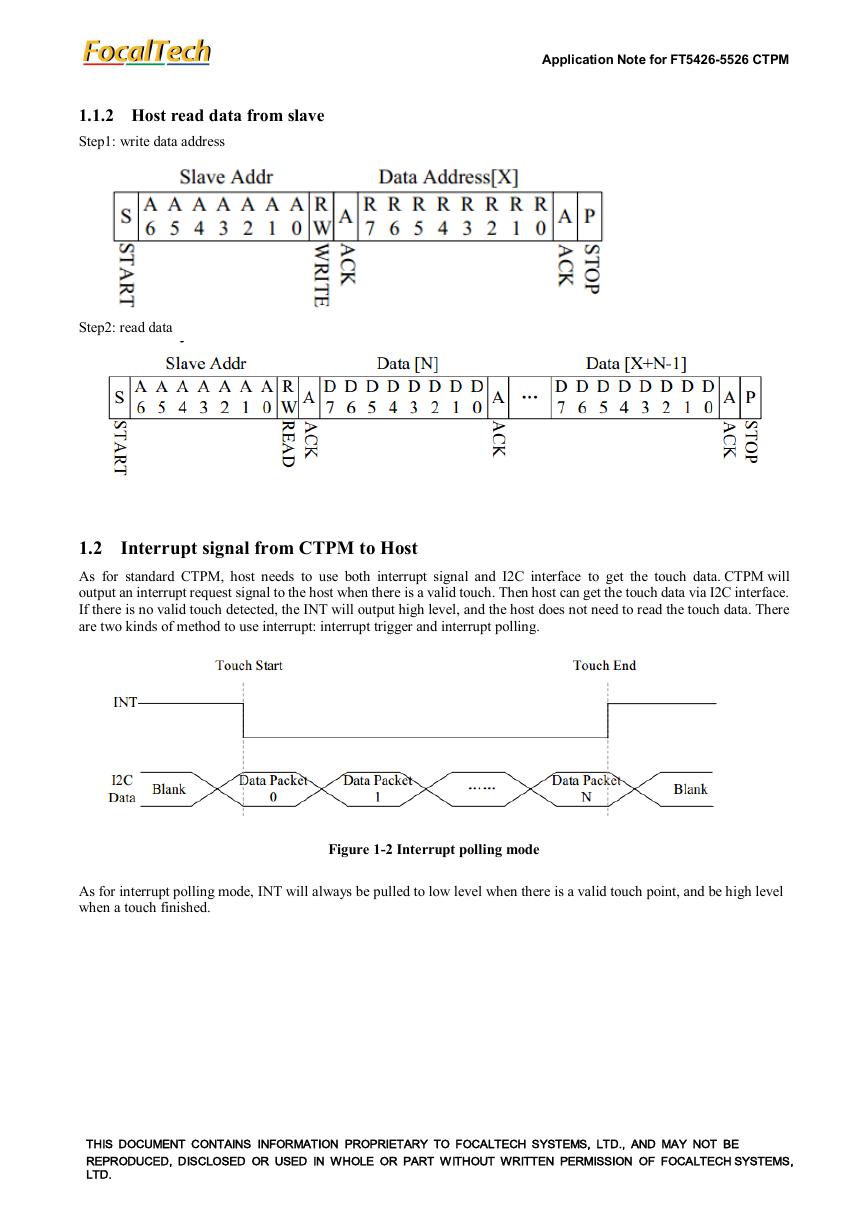
It is important to note that the SDA and SCL must connect with a pull-high resistor respectively before you read/write I2C
data.
1.1.1 Host write data to slave
THIS DOCUMENT CONTAINS INFORMATION PROPRIETARY TO FOCALTECH SYSTEMS, LTD., AND MAY NOT BE
REPRODUCED, DISCLOSED OR USED IN W HOLE OR PART W ITHOUT WRITTEN PERMISSION OF FOCALTECH SYSTEMS,
LTD.
�
Application Note for FT5426-5526 CTPM
1.1.2 Host read data from slave
Step1: write data address
Step2: read data
1.2 Interrupt signal from CTPM to Host
As for standard CTPM, host needs to use both interrupt signal and I2C interface to get the touch data. CTPM will
output an interrupt request signal to the host when there is a valid touch. Then host can get the touch data via I2C interface.
If there is no valid touch detected, the INT will output high level, and the host does not need to read the touch data. There
are two kinds of method to use interrupt: interrupt trigger and interrupt polling.
Figure 1-2 Interrupt polling mode
As for interrupt polling mode, INT will always be pulled to low level when there is a valid touch point, and be high level
when a touch finished.
THIS DOCUMENT CONTAINS INFORMATION PROPRIETARY TO FOCALTECH SYSTEMS, LTD., AND MAY NOT BE
REPRODUCED, DISCLOSED OR USED IN W HOLE OR PART W ITHOUT WRITTEN PERMISSION OF FOCALTECH SYSTEMS,
LTD.
�
Application Note for FT5426-5526 CTPM
Figure 1-3 Interrupt trigger mode
While for interrupt trigger mode, INT signal will be set to low if there is a touch detected. But whenever an update of valid
touch data, CTPM will produce a valid pulse on INT port for INT signal, and host can read the touch data periodically
according to the frequency of this pulse. In this mode, the pulse frequency is the touch data updating rate
1.3 Reset signal from Host to CTPM.
Host can send the reset signal via RST port to reset FT5426-5526. The reset signal should not be set to low while in normal
working mode. The RST port can also be used to active the CTPM in hibernate mode. Note that the reset pulse width
should be more than 1ms.
THIS DOCUMENT CONTAINS INFORMATION PROPRIETARY TO FOCALTECH SYSTEMS, LTD., AND MAY NOT BE
REPRODUCED, DISCLOSED OR USED IN W HOLE OR PART W ITHOUT WRITTEN PERMISSION OF FOCALTECH SYSTEMS,
LTD.
�
Application Note for FT5426-5526 CTPM
2 Standard Application Circuit
Table 2-1 is a brief summary of the FT5426-5526 application features.
Table 2-1 Brief features of FT5426-5526
IC Type
Operating Voltage(V)
Channel
Panel Size
Touch points
Interface
Report rate
Package (mm)
FT5426DQ8
2.8 ~ 3.6
28 TX + 16 RX
FT5526EEZ
2.8 ~ 3.6
35 TX + 21 RX
≤8”
10
I2C
>100Hz
≤10.1”
10
I2C
>100Hz
QFN 56L 6x6x0.6mm
Pitch =0.35mm
QFN 68L 8x8x0.8mm
Pitch =0.4mm
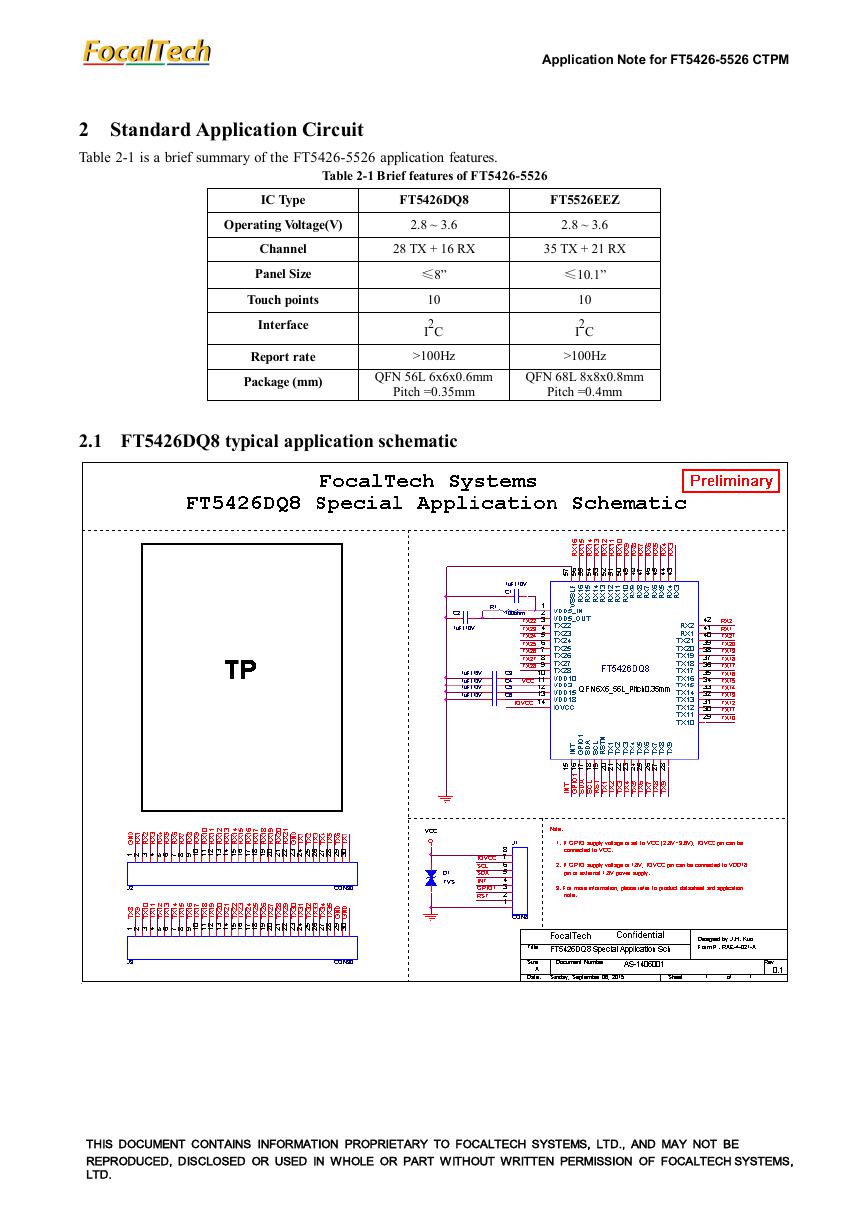
2.1 FT5426DQ8 typical application schematic
THIS DOCUMENT CONTAINS INFORMATION PROPRIETARY TO FOCALTECH SYSTEMS, LTD., AND MAY NOT BE
REPRODUCED, DISCLOSED OR USED IN W HOLE OR PART W ITHOUT WRITTEN PERMISSION OF FOCALTECH SYSTEMS,
LTD.
�
Application Note for FT5426-5526 CTPM
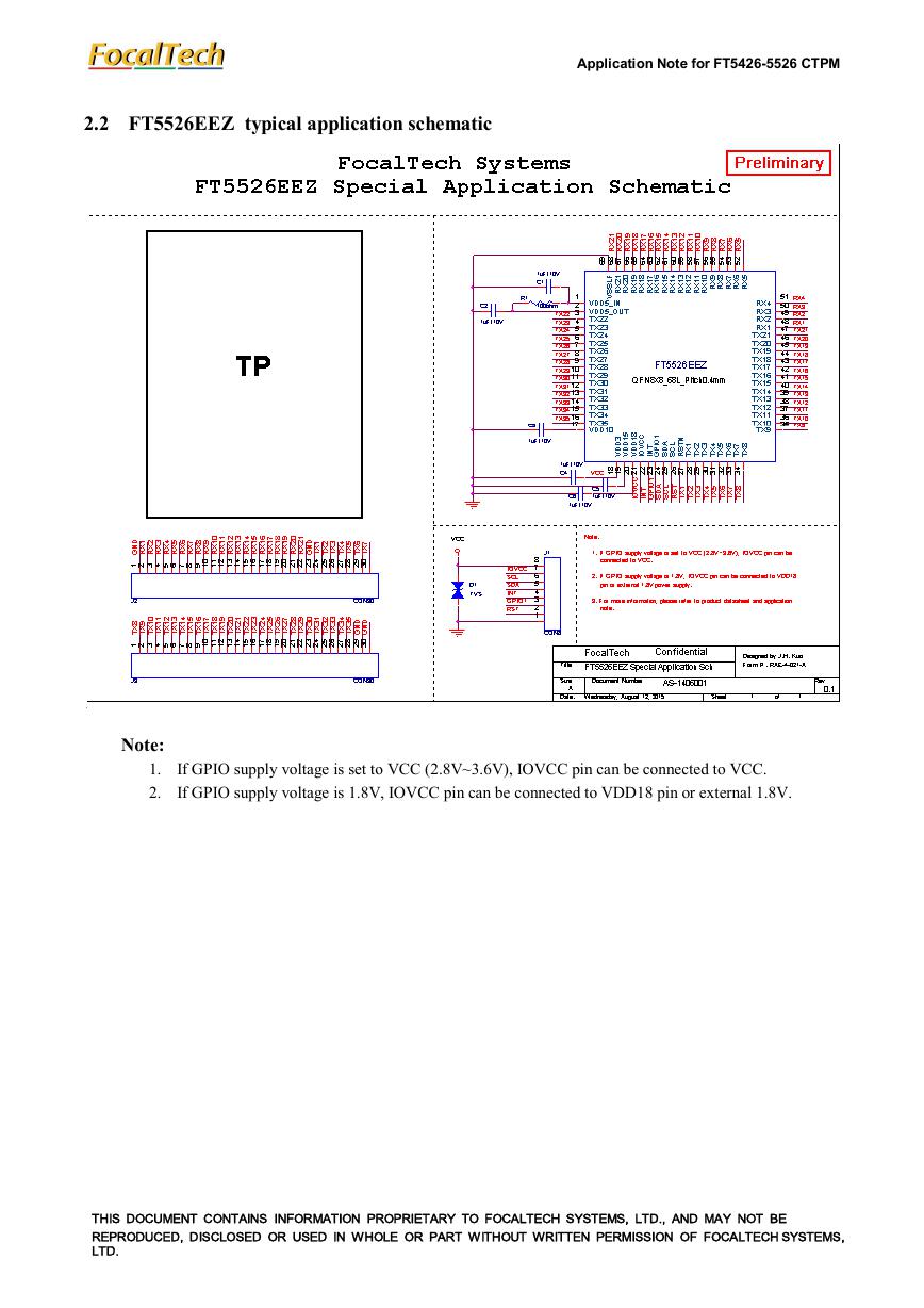
2.2 FT5526EEZ typical application schematic
Note:
1.
2.
If GPIO supply voltage is set to VCC (2.8V~3.6V), IOVCC pin can be connected to VCC.
If GPIO supply voltage is 1.8V, IOVCC pin can be connected to VDD18 pin or external 1.8V.
THIS DOCUMENT CONTAINS INFORMATION PROPRIETARY TO FOCALTECH SYSTEMS, LTD., AND MAY NOT BE
REPRODUCED, DISCLOSED OR USED IN W HOLE OR PART W ITHOUT WRITTEN PERMISSION OF FOCALTECH SYSTEMS,
LTD.
�




 V2版本原理图(Capacitive-Fingerprint-Reader-Schematic_V2).pdf
 摄像头工作原理.doc
 VL53L0X简要说明(En.FLVL53L00216).pdf
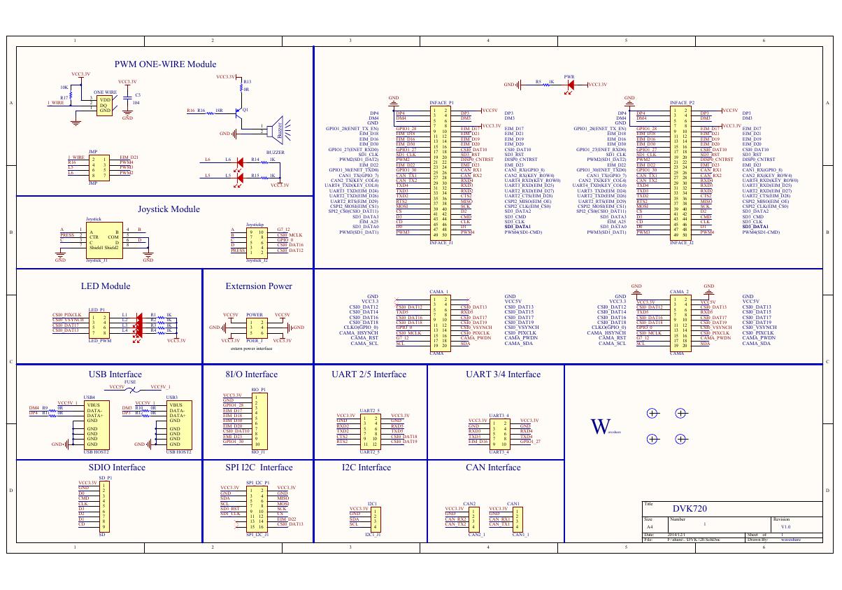 原理图(DVK720-Schematic).pdf
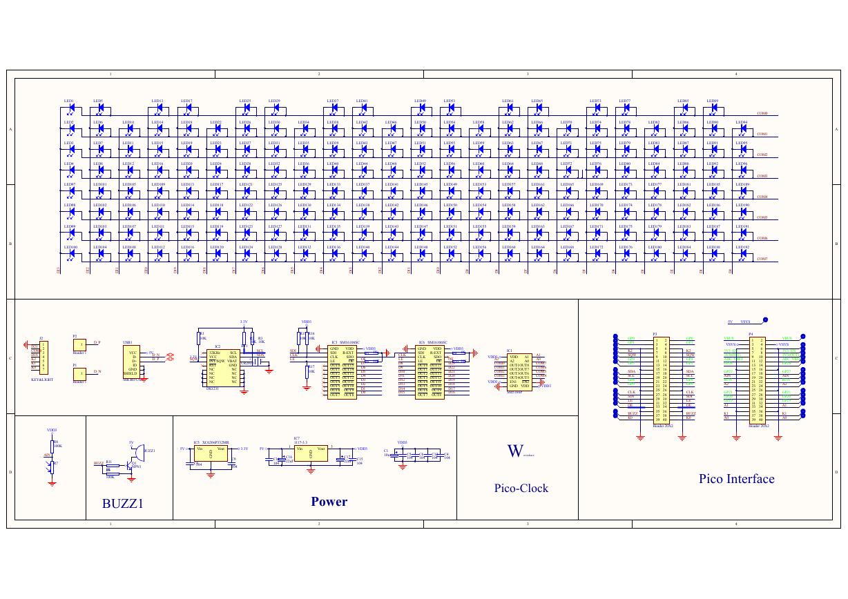 原理图(Pico-Clock-Green-Schdoc).pdf
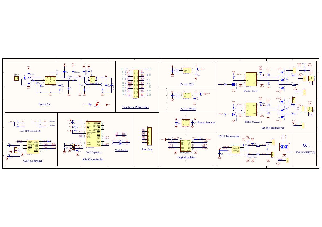 原理图(RS485-CAN-HAT-B-schematic).pdf
 File:SIM7500_SIM7600_SIM7800 Series_SSL_Application Note_V2.00.pdf
 ADS1263(Ads1262).pdf
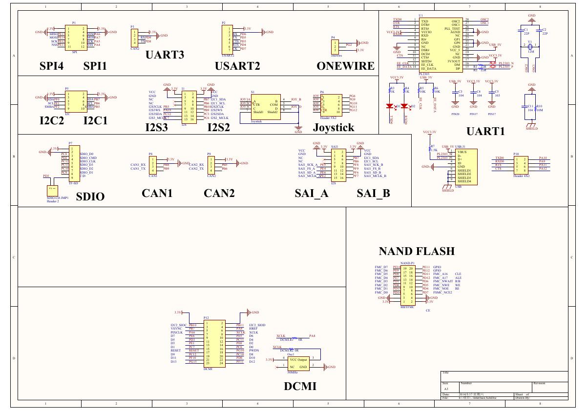 原理图(Open429Z-D-Schematic).pdf
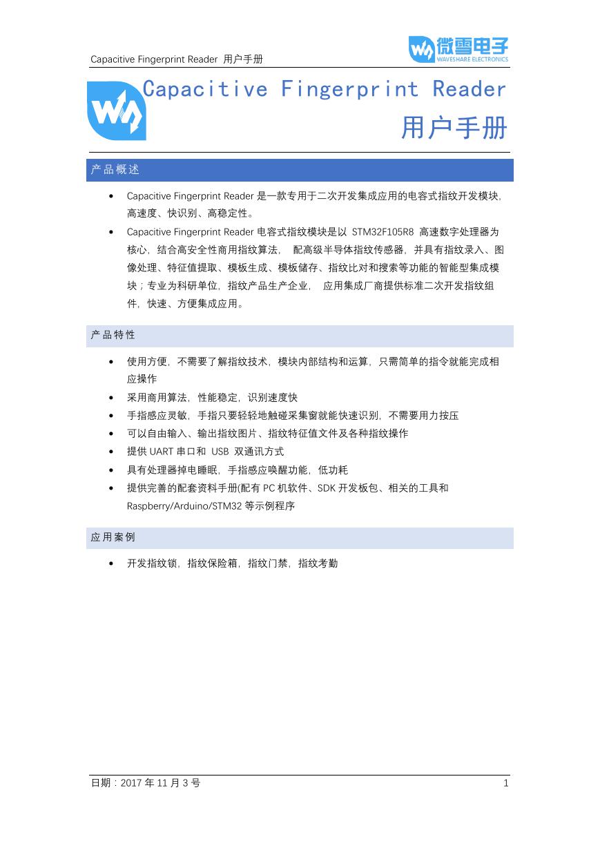 用户手册(Capacitive_Fingerprint_Reader_User_Manual_CN).pdf
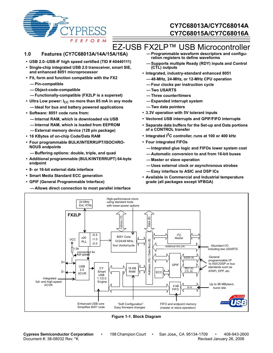 CY7C68013A(英文版)(CY7C68013A).pdf
 TechnicalReference_Dem.pdf