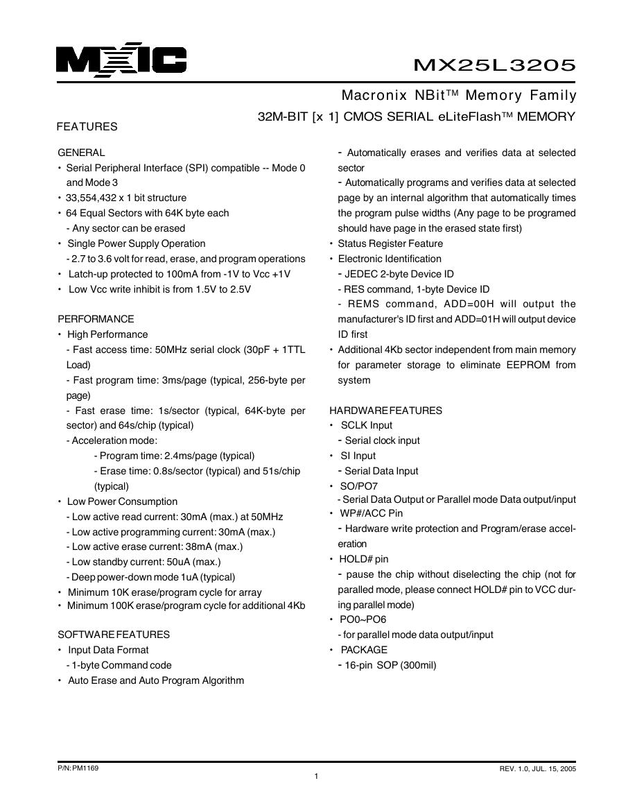
MX25L3205
Macronix NBitTM Memory Family
32M-BIT [x 1] CMOS SERIAL eLiteFlashTM MEMORY
FEATURES
GENERAL
• Serial Peripheral Interface (SPI) compatible -- Mode 0
and Mode 3
33,554,432 x 1 bit structure
64 Equal Sectors with 64K byte each
- Any sector can be erased
Single Power Supply Operation
- 2.7 to 3.6 volt for read, erase, and program operations
Latch-up protected to 100mA from -1V to Vcc +1V
Low Vcc write inhibit is from 1.5V to 2.5V
PERFORMANCE
High Performance
- Fast access time: 50MHz serial clock (30pF + 1TTL
Load)
- Fast program time: 3ms/page (typical, 256-byte per
page)
- Fast erase time: 1s/sector (typical, 64K-byte per
sector) and 64s/chip (typical)
- Acceleration mode:
- Program time: 2.4ms/page (typical)
- Erase time: 0.8s/sector (typical) and 51s/chip
(typical)
Low Power Consumption
- Low active read current: 30mA (max.) at 50MHz
- Low active programming current: 30mA (max.)
- Low active erase current: 38mA (max.)
- Low standby current: 50uA (max.)
- Deep power-down mode 1uA (typical)
Minimum 10K erase/program cycle for array
Minimum 100K erase/program cycle for additional 4Kb
SOFTWARE FEATURES
Input Data Format
- 1-byte Command code
Auto Erase and Auto Program Algorithm
- Automatically erases and verifies data at selected
sector
- Automatically programs and verifies data at selected
page by an internal algorithm that automatically times
the program pulse widths (Any page to be programed
should have page in the erased state first)
• Status Register Feature
Electronic Identification
- JEDEC 2-byte Device ID
- RES command, 1-byte Device ID
- REMS command, ADD=00H will output the
manufacturer's ID first and ADD=01H will output device
ID first
Additional 4Kb sector independent from main memory
for parameter storage to eliminate EEPROM from
system
HARDWARE FEATURES
SCLK Input
- Serial clock input
SI Input
- Serial Data Input
SO/PO7
- Serial Data Output or Parallel mode Data output/input
WP#/ACC Pin
- Hardware write protection and Program/erase accel-
eration
HOLD# pin
- pause the chip without diselecting the chip (not for
paralled mode, please connect HOLD# pin to VCC dur-
ing parallel mode)
PO0~PO6
- for parallel mode data output/input
PACKAGE
- 16-pin SOP (300mil)
P/N: PM1169
1
REV. 1.0, JUL. 15, 2005
�
MX25L3205
GENERAL DESCRIPTION
The MX25L3205 is a CMOS 33,554,432 bit serial
eLiteFlashTM Memory, which is configured as 4,194,304 x
8 internally. The MX25L3205 features a serial peripheral
interface and software protocol allowing operation on a
simple 3- wire bus. The three bus signals are a clock input
(SCLK), a serial data input (SI), and a serial data output
(SO). SPI access to the device is enabled by CS# input.
The MX25L3205 provide sequential read operation on
whole chip. User may start to read from any byte of the
array. While the end of the array is reached, the device will
wrap around to the beginning of the array and continuously
outputs data until CS# goes high.
After program/erase command is issued, auto program/
erase algorithms which program/erase and verify the
specified page locations will be executed. Program com-
mand is executed on a page (256 bytes) basis, and erase
command is executed on both chip and sector (64K bytes)
basis.
To provide user with ease of interface, a status register is
included to indicate the status of the chip. The status read
command can be issued to detect completion and error
flag status of a program or erase operation.
To increase user's factory throughputs, a parallel mode is
provided. The performance of read/program is dramatically
improved than serial mode on programmer machine.
When the device is not in operation and CS# is high, it is
put in standby mode and draws less than 50uA DC current.
The additional 4Kb sector with 100K erase/program endur-
ance cycles is suitable for parameter storage and replaces
the EEPROM on system.
The MX25L3205 utilizes MXIC's proprietary memory cell
which reliably stores memory contents even after 10K
program and erase cycles.
PIN CONFIGURATIONS
PIN DESCRIPTION
16-PIN SOP (300 mil)
HOLD#
VCC
NC
PO2
PO1
PO0
CS#
SO/PO7
1
2
3
4
5
6
7
8
16
15
14
13
12
11
10
9
SCLK
SI
PO6
PO5
PO4
PO3
GND
WP#/ACC
SYMBOL
CS#
SI
SO/PO7(1) Serial Data Output or Parallel Data
DESCRIPTION
Chip Select
Serial Data Input
output/input
Clock Input
SCLK
HOLD#(2) Hold, to pause the serial communication
(HOLD# is not for parallel mode)
WP#/ACC Write Protection: connect to GND;
12V for program/erase acceleration:
connect to 12V
+ 3.3V Power Supply
Ground
VCC
GND
PO0~PO6 Parallel data output/input (PO0~PO6 can
NC
be connected to NC in serial mode)
No Internal Connection
Note:
1. PO0~PO7 are not provided on 8-LAND SON package.
2. HOLD# is recommended to connect to VCC during
parallel mode.
P/N: PM1169
2
REV. 1.0, JUL. 15, 2005
�
BLOCK DIAGRAM
MX25L3205
Address
Generator
Memory Array
-
X
D
e
c
o
d
e
r
a
d
d
i
t
i
o
n
a
l
4
K
b
SI
Data
Register
Y-Decoder
SRAM
Buffer
CS#, ACC,
WP#,HOLD#
Mode
Logic
State
Machine
HV
Generator
SCLK
Clock Generator
Sense
Amplifier
Output
Buffer
SO
P/N: PM1169
3
REV. 1.0, JUL. 15, 2005
�
MX25L3205
To avoid unexpected changes by system power supply
transition, the Power-On Reset and an internal timer
(tPUW) can protect the device.
Before the Program, Erase, and Write Status Register
execution, instruction length will be checked on follow-
ing the clock pulse number to be multiple of eight base.
Write Enable (WREN) instruction must set to Write
Enable Latch (WEL) bit before writing other instructions
to modify data. The WEL bit will return to reset state by
following situations:
- Power-up
- Write Disable (WRDI) instruction completion
- Write Status Register (WRSR) instruction completion
- Page Program (PP) instruction completion
- Sector Erase (SE) instruction completion
- Chip Erase (CE) instruction completion
The Software Protected Mode (SPM) use (BP2, BP1,
BP0) bits to allow part of memory to be protected as
read only.
The Hardware Protected Mode (HPM) use WP# to
protect the (BP2, BP1, BP0) bits and SRWD bit.
Deep-Power Down Mode also protects the device by
ignoring all instructions except Release from Deep-
Power Down (RDP) instruction and RES instruction.
DATA PROTECTION
The MX25L3205 are designed to offer protection against
accidental erasure or programming caused by spurious
system level signals that may exist during power
transition. During power up the device automatically resets
the state machine in the Read mode. In addition, with its
control register architecture, alteration of the memory
contents only occurs after successful completion of
specific command sequences. The device also
incorporates several features to prevent inadvertent write
cycles resulting from VCC power-up and power-down
transition or system noise.
Power-On Reset and an internal timer (tPUW) can
provide protection against inadvertant changes while
the power supply is outside the operating specification.
Program, Erase and Write Status Register instructions
are checked that they consist of a number of clock
pulses that is a multiple of eight, before they are
accepted for execution.
All instructions that modify data must be preceded by
a Write Enable (WREN) instruction to set the Write
Enable Latch (WEL) bit . This bit is returned to its reset
state by the following events:
- Power-up
- Write Disable (WRDI) instruction completion
- Write Status Register (WRSR) instruction completion
- Page Program (PP) instruction completion
- Sector Erase (SE) instruction completion
- Chip Erase (CE) instruction completion
The Block Protect (BP2, BP1, BP0) bits allow part of
the memory to be configured as readonly. This is the
Software Protected Mode (SPM).
The Write Protect (WP#) signal allows the Block
Protect (BP2, BP1, BP0) bits and Status Register
Write Disable (SRWD) bit to be protected. This is the
Hardware Protected Mode (HPM).
In addition to the low power consumption feature, the
Deep Power-down mode offers extra software protec-
tion from inadvertent Write, Program and Erase in-
structions, as all instructions are ignored except one
particular instruction (the Release from Deep
Powerdown instruction).
P/N: PM1169
4
REV. 1.0, JUL. 15, 2005
�
MX25L3205
Table 1. Protected Area Sizes
Status bit
BP2
BP1
BP0
0
0
0
0
1
1
1
1
0
0
1
1
0
0
1
1
0
1
0
1
0
1
0
1
Protection Area
32Mb
None
Upper 64th (Sector 63)
Upper 32nd (two sectors: 62 and 63)
Upper sixteenth (four sectors: 60 to 63)
Upper eighth (eight sectors: 56 to 63)
Upper quarter (sixteen sectors: 48 to 63)
Upper half (thirty-two sectors: 32 to 63)
All
Note:
1. The device is ready to accept a Chip Erase instruction if, and only if, all Block Protect (BP2, BP1, BP0) are 0.
P/N: PM1169
5
REV. 1.0, JUL. 15, 2005
�
MX25L3205
HOLD FEATURE
HOLD# pin signal goes low to hold any serial communications with the device. The HOLD feature will not stop the operation
of write status register, programming, or erasing in progress.
The operation of HOLD requires Chip Select(CS#) keeping low and starts on falling edge of HOLD# pin signal while Serial
Clock (SCLK) signal is being low (if Serial Clock signal is not being low, HOLD operation will not start until Serial Clock
signal being low). The HOLD condition ends on the rising edge of HOLD# pin signal while Serial Clock(SCLK) signal is
being low( if Serial Clock signal is not being low, HOLD operation will not end until Serial Clock being low), see Figure 1.
Figure 1. Hold Condition Operation
SCLK
HOLD#
Hold
Condition
(standard use)
Hold
Condition
(non-standard use)
The Serial Data Output (SO) is high impedance, both Serial Data Input (SI) and Serial Clock (SCLK) are don't care during
the HOLD operation. If Chip Select (CS#) signal goes high during HOLD operation, it has the effect on resetting the internal
logic of the device. It is necessary to drive HOLD# signal to high, and then to drive CS# to low for restarting communication
with the device.
The HOLD operation is not recommended to use during parallel mode.
PROGRAM/ERASE ACCELERATION
To activate the program/erase acceleration function requires ACC pin connecting to 12V voltage (see Figure 2), and then
to be followed by the normal program/erase process. By utilizing the program/erase acceleration operation, the
performances are improved as shown on table of "ERASE AND PROGRAM PERFORMACE".
Figure 2. ACCELERATED PROGRAM TIMING DIAGRAM
VHH
12V
VIL or VIH
ACC
tVHH
Note: tVHH (VHH Rise and Fall Time) min. 250ns
VIL or VIH
tVHH
P/N: PM1169
6
REV. 1.0, JUL. 15, 2005
�
Table 2. COMMAND DEFINITION
MX25L3205
COMMAND WREN
(write
(byte)
Enable)
06 Hex
WRDI
(write
disable)
04 Hex
RDID
(read ident-
ification)
9F Hex
READ
WRSR
RDSR
(read status (write status (read data) (fast read Mode
register)
05 Hex
register)
01 Hex
Fast Read Parallel
55 Hex
03 Hex
AD1
AD2
AD3
data)
0B Hex
AD1
AD2
AD3
x
1st
2nd
3rd
4th
5th
Action
sets the
(WEL)
write
enable
latch bit
to read out
the status
reset the output the
(WEL)
write
enable
latch bit
manufacturer
ID and 2-byte register
device ID
to write new n bytes
values to the read out
status register until
CS# goes
high
Enter and
stay in
Parallel
Mode until
power off
COMMAND SE
(byte)
CE
(Chip
PP
(Page
DP
(Deep
EN4K
(Enter
(Sector
Erase) Erase) Program) Power 4Kb
RDP
(Release
from Deep
EX4K
(Exit
4Kb
sector) Power-down)
RES(Read REMS (Read
Electronic Electronic
ID)
Manufacturer
& Device ID)
90 Hex
Down) sector)
B9 Hex A5 Hex B5 Hex AB Hex
60 or
20 or
D8 Hex C7 Hex
AD1
AD2
AD3
02 Hex
AD1
AD2
AD3
1st
2nd
3rd
4th
5th
Action
AB Hex
x
x
x
x
x
ADD (1)
Output the
manufacturer
ID and device
ID
Exit
the
Enter
the
additional additional
4Kb
sector
4Kb
sector
(1) ADD=00H will output the manufacturer's ID first and ADD=01H will output device ID first
P/N: PM1169
7
REV. 1.0, JUL. 15, 2005
�
Table 3. Memory Organization
MX25L3205
Sector Address Range
63
62
61
60
59
58
57
56
55
54
53
52
51
50
49
48
47
46
45
44
43
42
41
40
39
38
37
36
35
34
33
32
3F0000h
3E0000h
3D0000h
3C0000h
3B0000h
3A0000h
390000h
380000h
370000h
360000h
350000h
340000h
330000h
320000h
310000h
300000h
2F0000h
2E0000h
2D0000h
2C0000h
2B0000h
2A0000h
290000h
280000h
270000h
260000h
250000h
240000h
230000h
220000h
210000h
200000h
3FFFFFh
3EFFFFh
3DFFFFh
3CFFFFh
3BFFFFh
3AFFFFh
39FFFFh
38FFFFh
37FFFFh
36FFFFh
35FFFFh
34FFFFh
33FFFFh
32FFFFh
31FFFFh
30FFFFh
2FFFFFh
2EFFFFh
2DFFFFh
2CFFFFh
2BFFFFh
2AFFFFh
29FFFFh
28FFFFh
27FFFFh
26FFFFh
25FFFFh
24FFFFh
23FFFFh
22FFFFh
21FFFFh
20FFFFh
Sector Address Range
31
30
29
28
27
26
25
24
23
22
21
20
19
18
17
16
15
14
13
12
11
10
9
8
7
6
5
4
3
2
1
0
1F0000h
1E0000h
1D0000h
1C0000h
1B0000h
1A0000h
190000h
180000h
170000h
160000h
150000h
140000h
130000h
120000h
110000h
100000h
0F0000h
0E0000h
0D0000h
0C0000h
0B0000h
0A0000h
090000h
080000h
070000h
060000h
050000h
040000h
030000h
020000h
010000h
000000h
1FFFFFh
1EFFFFh
1DFFFFh
1CFFFFh
1BFFFFh
1AFFFFh
19FFFFh
18FFFFh
17FFFFh
16FFFFh
15FFFFh
14FFFFh
13FFFFh
12FFFFh
11FFFFh
10FFFFh
0FFFFFh
0EFFFFh
0DFFFFh
0CFFFFh
0BFFFFh
0AFFFFh
09FFFFh
08FFFFh
07FFFFh
06FFFFh
05FFFFh
04FFFFh
03FFFFh
02FFFFh
01FFFFh
00FFFFh
P/N: PM1169
8
REV. 1.0, JUL. 15, 2005
�


 V2版本原理图(Capacitive-Fingerprint-Reader-Schematic_V2).pdf
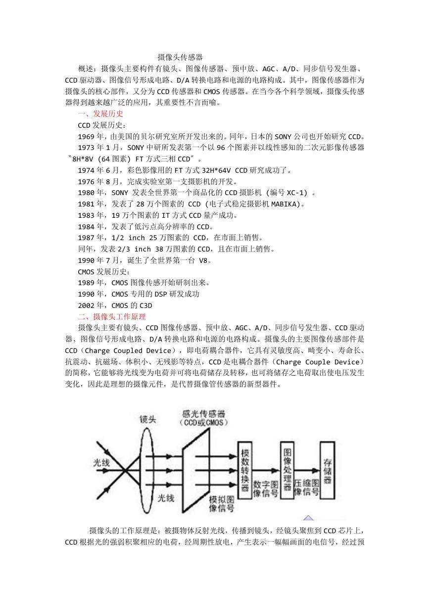 摄像头工作原理.doc
 VL53L0X简要说明(En.FLVL53L00216).pdf
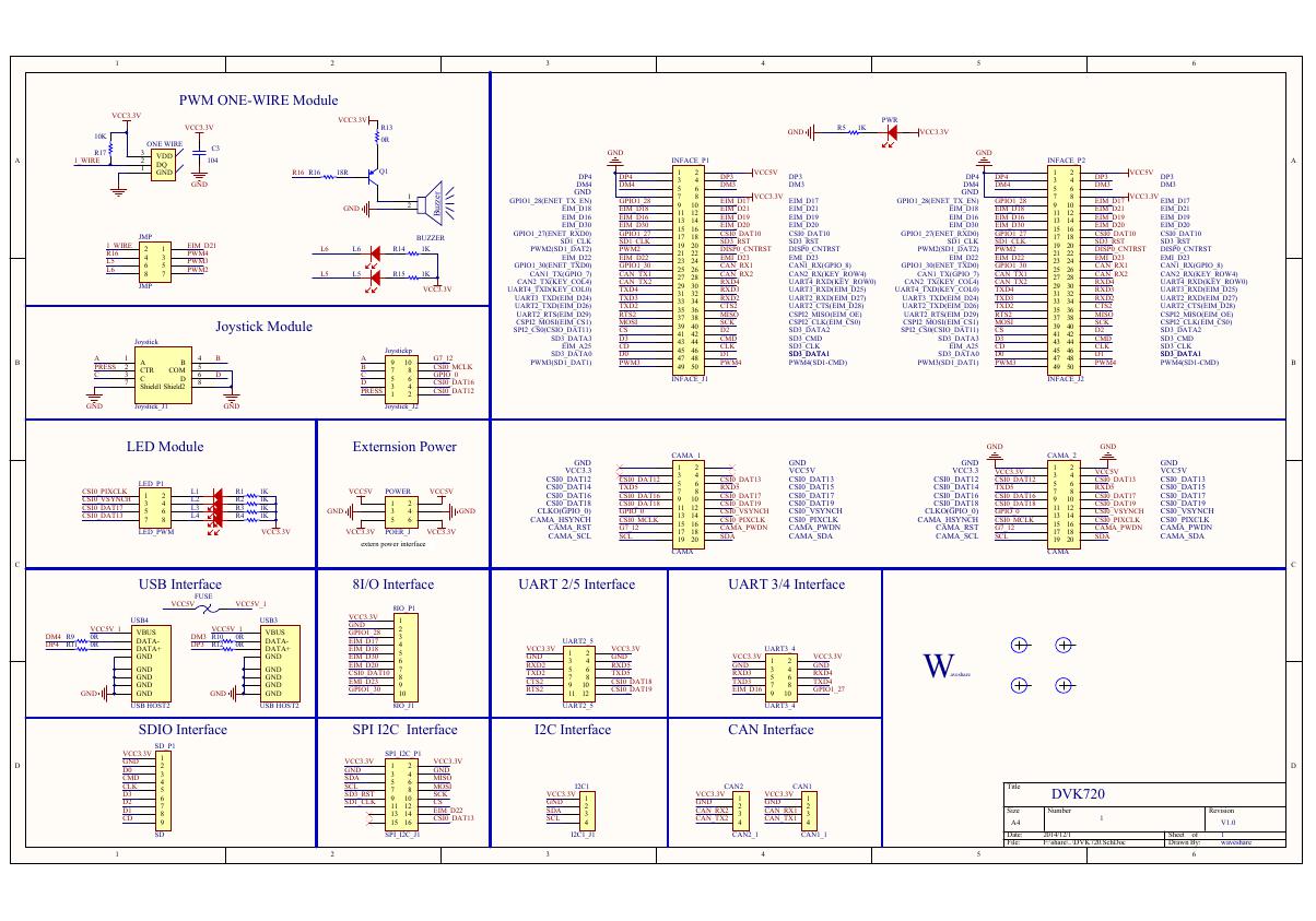 原理图(DVK720-Schematic).pdf
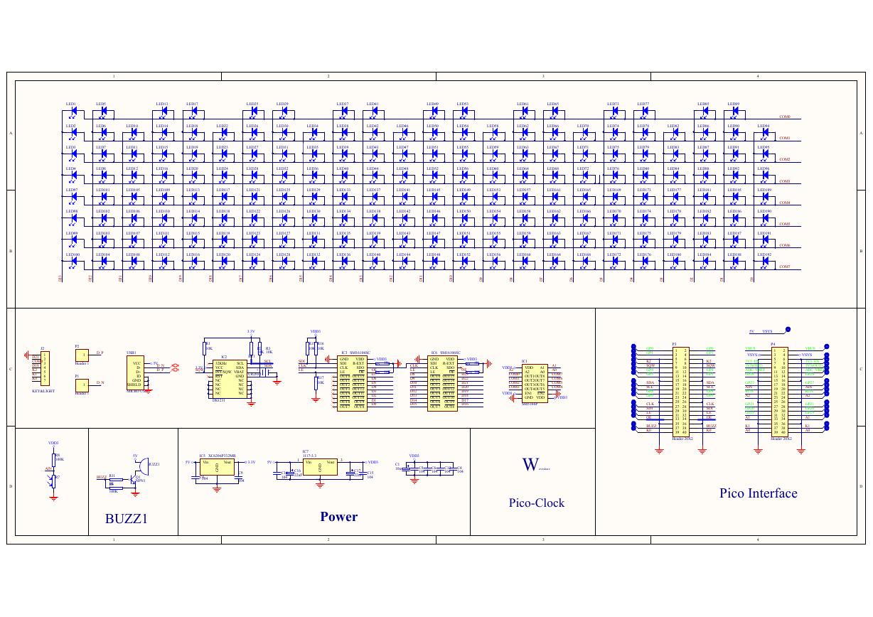 原理图(Pico-Clock-Green-Schdoc).pdf
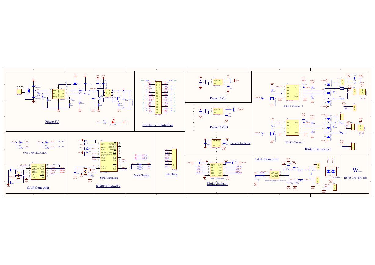 原理图(RS485-CAN-HAT-B-schematic).pdf
 File:SIM7500_SIM7600_SIM7800 Series_SSL_Application Note_V2.00.pdf
 ADS1263(Ads1262).pdf
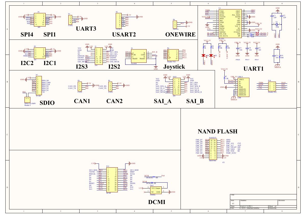 原理图(Open429Z-D-Schematic).pdf
 用户手册(Capacitive_Fingerprint_Reader_User_Manual_CN).pdf
 CY7C68013A(英文版)(CY7C68013A).pdf
 TechnicalReference_Dem.pdf