logo资料库

SIM868_Series_Hardware_Design_V1.06.pdf

第1页 / 共72页
第2页 / 共72页
第3页 / 共72页
第4页 / 共72页
第5页 / 共72页
第6页 / 共72页
第7页 / 共72页
第8页 / 共72页
资料共72页,剩余部分请下载后查看
Introduction
SIM868 Overview
SIM868 Key Features
Operating Modes
Functional Diagram
Package Information
Pin Out Diagram
Pin Description
Package Dimensions
Application Modes of SIM868
All-in-one Mode
Stand-alone Mode
Application Interface of GSM
Power Supply of GSM
Reference Circuit of GSM Power Supply
Power on/off GSM Part
Power on GSM
Power off GSM
Power off GSM by the PWRKEY Pin
Power off GSM by AT Command
Restart GSM by PWRKEY:
Power Saving Mode of GSM
Minimum Functionality Mode of GSM Part
Sleep Mode 1 (AT+CSCLK=1)
Wake Up GSM from Sleep Mode 1
Sleep Mode 2 (AT+CSCLK=2)
Wake Up GSM from Sleep Mode 2
Serial Port of GSM
Function of Serial Port
Serial Interfaces
Debug Interface
Software Upgrade of GSM
UART1_RI Behaviors
Audio Interfaces
Speaker Interfaces Configuration
Microphone Interfaces Configuration
Audio Electronic Characteristic
TDD Noise of GSM
SIM Card Interface
SIM Card Application
SIM Card Design Guide
Design Considerations for SIM Card Holder
SD Interface
I2C Bus
ADC
Network Status Indication
Operating Status Indication
RF Synchronization Signal
Antenna Interface of GSM
Bluetooth Antenna Interface
Bluetooth Low Energy (BLE)
Application Interface of GNSS
GNSS Overview
Power Supply of GNSS
Backup Power of GNSS
Power on/off GNSS
Serial Port of GNSS
Software Upgrade of GNSS
1PPS Output
Antenna Interface
Passive Antenna
Active Antenna
Operation Modes of GNSS
A-GPS
Easy Mode
EPO
Fast-Fix
Multi-tone AIC
SBAS
PCB Layout
Pin Assignment
Principle of PCB Layout
Antenna Interface
Power Supply
SIM Card Interface
Audio Interface
Electrical, Reliability and Radio Characteristics
Absolute Maximum Ratings
Recommended Operating Conditions
Digital Interface Characteristics
SIM Card Interface Characteristics
SIM_VDD Characteristics
VDD_EXT Characteristics
Current Consumption(GSM_VBAT=4.0V)
Electro-Static Discharge
Radio Characteristics
Module RF Output Power
Module RF Receive Sensitivity
Module Operating Frequencies
Manufacturing
Top and Bottom View of SIM868
Typical Solder Reflow Profile
The Moisture Sensitivity Level
Baking Requirements
Packaging
Appendix
Related Documents
Terms and Abbreviations
Safety Caution
SIM868_Series_Hardware_Design_V1.06 SIMCOM CONFIDENTIAL FILE
Smart Machine Smart Decision Document Title SIM868 Series Hardware Design Version Date Status V1.06 2017-07-13 Release Document Control ID SIM868_Series_Hardware_Design_V1.06 General Notes SIMCom offers this information as a service to its customers, to support application and engineering efforts that use the products designed by SIMCom. The information provided is based upon requirements specifically provided to SIMCom by the customers. SIMCom has not undertaken any independent search for additional relevant information, including any information that may be in the customer’s possession. Furthermore, system validation of this product designed by SIMCom within a larger electronic system remains the responsibility of the customer or the customer’s system integrator. All specifications supplied herein are subject to change. Copyright This document contains proprietary technical information which is the property of SIMCom Limited, copying of this document and giving it to others and the using or communication of the contents thereof, are forbidden without express authority. Offenders are liable to the payment of damages. All rights reserved in the event of grant of a patent or the registration of a utility model or design. All specification supplied herein are subject to change without notice at any time. Copyright © Shanghai SIMCom Wireless Solutions Ltd. 2017 SIM868_Series_Hardware_Design_V1.06 1 2017-07-13 SIMCOM CONFIDENTIAL FILE
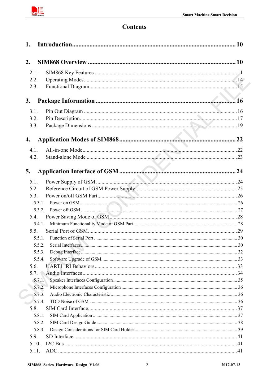
Smart Machine Smart Decision Contents 1. Introduction ........................................................................................................ 10 2. SIM868 Overview .............................................................................................. 10 2.1. SIM868 Key Features ......................................................................................................... 11 2.2. Operating Modes ................................................................................................................. 14 Functional Diagram............................................................................................................. 15 2.3. 3. Package Information ......................................................................................... 16 Pin Out Diagram ................................................................................................................. 16 3.1. Pin Description .................................................................................................................... 17 3.2. 3.3. Package Dimensions ........................................................................................................... 19 4. Application Modes of SIM868 .......................................................................... 22 4.1. All-in-one Mode .................................................................................................................. 22 Stand-alone Mode ............................................................................................................... 23 4.2. 5.4. 5. Application Interface of GSM .......................................................................... 24 5.1. Power Supply of GSM ........................................................................................................ 24 5.2. Reference Circuit of GSM Power Supply ........................................................................... 25 5.3. Power on/off GSM Part ....................................................................................................... 26 5.3.1. Power on GSM .................................................................................................................................... 26 5.3.2. Power off GSM ................................................................................................................................... 27 Power Saving Mode of GSM .............................................................................................. 28 5.4.1. Minimum Functionality Mode of GSM Part ....................................................................................... 28 Serial Port of GSM .............................................................................................................. 29 5.5.1. Function of Serial Port ........................................................................................................................ 30 5.5.2. Serial Interfaces ................................................................................................................................... 30 5.5.3. Debug Interface ................................................................................................................................... 32 5.5.4. Software Upgrade of GSM .................................................................................................................. 33 5.6. UART1_RI Behaviors ......................................................................................................... 33 5.7. Audio Interfaces .................................................................................................................. 34 5.7.1. Speaker Interfaces Configuration ........................................................................................................ 35 5.7.2. Microphone Interfaces Configuration ................................................................................................. 36 5.7.3. Audio Electronic Characteristic .......................................................................................................... 36 5.7.4. TDD Noise of GSM ............................................................................................................................ 36 SIM Card Interface.............................................................................................................. 37 5.8.1. SIM Card Application ......................................................................................................................... 37 5.8.2. SIM Card Design Guide ...................................................................................................................... 38 5.8.3. Design Considerations for SIM Card Holder ...................................................................................... 39 SD Interface ........................................................................................................................ 41 5.9. 5.10. I2C Bus ............................................................................................................................... 41 5.11. ADC .................................................................................................................................... 41 5.5. 5.8. SIM868_Series_Hardware_Design_V1.06 2 2017-07-13 SIMCOM CONFIDENTIAL FILE
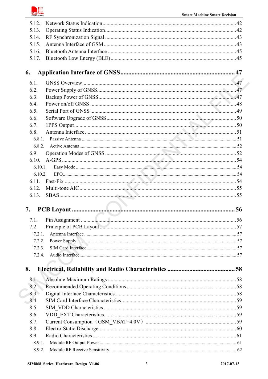
Smart Machine Smart Decision 5.12. Network Status Indication ................................................................................................... 42 5.13. Operating Status Indication ................................................................................................. 42 5.14. RF Synchronization Signal ................................................................................................. 43 5.15. Antenna Interface of GSM .................................................................................................. 43 5.16. Bluetooth Antenna Interface ............................................................................................... 45 5.17. Bluetooth Low Energy (BLE) ............................................................................................. 45 6. Application Interface of GNSS ......................................................................... 47 6.1. GNSS Overview .................................................................................................................. 47 6.2. Power Supply of GNSS....................................................................................................... 47 6.3. Backup Power of GNSS ...................................................................................................... 47 6.4. Power on/off GNSS ............................................................................................................ 48 Serial Port of GNSS ............................................................................................................ 49 6.5. 6.6. Software Upgrade of GNSS ................................................................................................ 50 6.7. 1PPS Output ........................................................................................................................ 50 6.8. Antenna Interface ................................................................................................................ 51 6.8.1. Passive Antenna .................................................................................................................................. 51 6.8.2. Active Antenna .................................................................................................................................... 52 6.9. Operation Modes of GNSS ................................................................................................. 52 6.10. A-GPS ................................................................................................................................. 54 Easy Mode ....................................................................................................................................... 54 EPO .................................................................................................................................................. 54 6.11. Fast-Fix ............................................................................................................................... 54 6.12. Multi-tone AIC .................................................................................................................... 55 6.13. SBAS ................................................................................................................................... 55 6.10.1. 6.10.2. 7. PCB Layout ........................................................................................................ 56 Pin Assignment ................................................................................................................... 56 7.1. 7.2. Principle of PCB Layout ..................................................................................................... 57 7.2.1. Antenna Interface ................................................................................................................................ 57 7.2.2. Power Supply ...................................................................................................................................... 57 7.2.3. SIM Card Interface .............................................................................................................................. 57 7.2.4. Audio Interface .................................................................................................................................... 57 8. Electrical, Reliability and Radio Characteristics ........................................... 58 8.1. Absolute Maximum Ratings ............................................................................................... 58 8.2. Recommended Operating Conditions ................................................................................. 58 8.3. Digital Interface Characteristics .......................................................................................... 58 8.4. SIM Card Interface Characteristics ..................................................................................... 59 8.5. SIM_VDD Characteristics .................................................................................................. 59 8.6. VDD_EXT Characteristics.................................................................................................. 59 8.7. Current Consumption(GSM_VBAT=4.0V) ................................................................... 59 8.8. Electro-Static Discharge ...................................................................................................... 60 8.9. Radio Characteristics .......................................................................................................... 61 8.9.1. Module RF Output Power ................................................................................................................... 61 8.9.2. Module RF Receive Sensitivity ........................................................................................................... 62 SIM868_Series_Hardware_Design_V1.06 3 2017-07-13 SIMCOM CONFIDENTIAL FILE
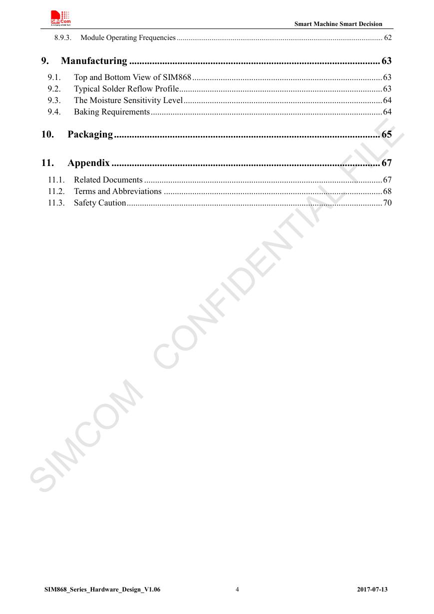
Smart Machine Smart Decision 8.9.3. Module Operating Frequencies ........................................................................................................... 62 9. Manufacturing ................................................................................................... 63 Top and Bottom View of SIM868 ....................................................................................... 63 9.1. 9.2. Typical Solder Reflow Profile ............................................................................................. 63 9.3. The Moisture Sensitivity Level ........................................................................................... 64 9.4. Baking Requirements .......................................................................................................... 64 10. Packaging ......................................................................................................... 65 11. Appendix .......................................................................................................... 67 11.1. Related Documents ............................................................................................................. 67 11.2. Terms and Abbreviations .................................................................................................... 68 11.3. Safety Caution ..................................................................................................................... 70 SIM868_Series_Hardware_Design_V1.06 4 2017-07-13 SIMCOM CONFIDENTIAL FILE
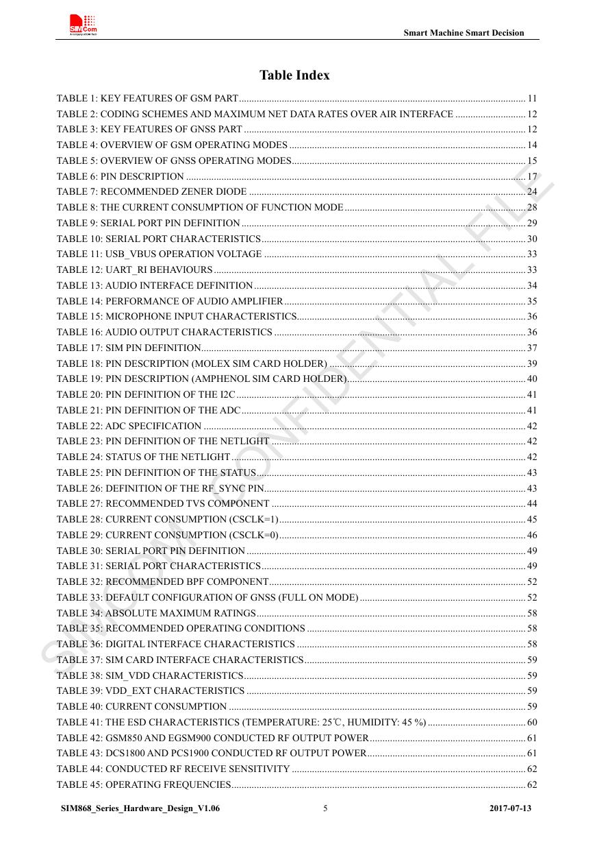
Smart Machine Smart Decision Table Index TABLE 1: KEY FEATURES OF GSM PART .................................................................................................................. 11 TABLE 2: CODING SCHEMES AND MAXIMUM NET DATA RATES OVER AIR INTERFACE ............................ 12 TABLE 3: KEY FEATURES OF GNSS PART ................................................................................................................ 12 TABLE 4: OVERVIEW OF GSM OPERATING MODES .............................................................................................. 14 TABLE 5: OVERVIEW OF GNSS OPERATING MODES ............................................................................................. 15 TABLE 6: PIN DESCRIPTION ....................................................................................................................................... 17 TABLE 7: RECOMMENDED ZENER DIODE .............................................................................................................. 24 TABLE 8: THE CURRENT CONSUMPTION OF FUNCTION MODE ........................................................................ 28 TABLE 9: SERIAL PORT PIN DEFINITION ................................................................................................................. 29 TABLE 10: SERIAL PORT CHARACTERISTICS ......................................................................................................... 30 TABLE 11: USB_VBUS OPERATION VOLTAGE ........................................................................................................ 33 TABLE 12: UART_RI BEHAVIOURS ............................................................................................................................ 33 TABLE 13: AUDIO INTERFACE DEFINITION ............................................................................................................ 34 TABLE 14: PERFORMANCE OF AUDIO AMPLIFIER ................................................................................................ 35 TABLE 15: MICROPHONE INPUT CHARACTERISTICS........................................................................................... 36 TABLE 16: AUDIO OUTPUT CHARACTERISTICS .................................................................................................... 36 TABLE 17: SIM PIN DEFINITION ................................................................................................................................. 37 TABLE 18: PIN DESCRIPTION (MOLEX SIM CARD HOLDER) .............................................................................. 39 TABLE 19: PIN DESCRIPTION (AMPHENOL SIM CARD HOLDER) ....................................................................... 40 TABLE 20: PIN DEFINITION OF THE I2C ................................................................................................................... 41 TABLE 21: PIN DEFINITION OF THE ADC ................................................................................................................. 41 TABLE 22: ADC SPECIFICATION ................................................................................................................................ 42 TABLE 23: PIN DEFINITION OF THE NETLIGHT ..................................................................................................... 42 TABLE 24: STATUS OF THE NETLIGHT ..................................................................................................................... 42 TABLE 25: PIN DEFINITION OF THE STATUS ........................................................................................................... 43 TABLE 26: DEFINITION OF THE RF_SYNC PIN........................................................................................................ 43 TABLE 27: RECOMMENDED TVS COMPONENT ..................................................................................................... 44 TABLE 28: CURRENT CONSUMPTION (CSCLK=1) .................................................................................................. 45 TABLE 29: CURRENT CONSUMPTION (CSCLK=0) .................................................................................................. 46 TABLE 30: SERIAL PORT PIN DEFINITION ............................................................................................................... 49 TABLE 31: SERIAL PORT CHARACTERISTICS ......................................................................................................... 49 TABLE 32: RECOMMENDED BPF COMPONENT ...................................................................................................... 52 TABLE 33: DEFAULT CONFIGURATION OF GNSS (FULL ON MODE) .................................................................. 52 TABLE 34: ABSOLUTE MAXIMUM RATINGS ........................................................................................................... 58 TABLE 35: RECOMMENDED OPERATING CONDITIONS ....................................................................................... 58 TABLE 36: DIGITAL INTERFACE CHARACTERISTICS ........................................................................................... 58 TABLE 37: SIM CARD INTERFACE CHARACTERISTICS ........................................................................................ 59 TABLE 38: SIM_VDD CHARACTERISTICS ................................................................................................................ 59 TABLE 39: VDD_EXT CHARACTERISTICS ............................................................................................................... 59 TABLE 40: CURRENT CONSUMPTION ...................................................................................................................... 59 TABLE 41: THE ESD CHARACTERISTICS (TEMPERATURE: 25℃, HUMIDITY: 45 %) ....................................... 60 TABLE 42: GSM850 AND EGSM900 CONDUCTED RF OUTPUT POWER .............................................................. 61 TABLE 43: DCS1800 AND PCS1900 CONDUCTED RF OUTPUT POWER ............................................................... 61 TABLE 44: CONDUCTED RF RECEIVE SENSITIVITY ............................................................................................. 62 TABLE 45: OPERATING FREQUENCIES ..................................................................................................................... 62 SIM868_Series_Hardware_Design_V1.06 5 2017-07-13 SIMCOM CONFIDENTIAL FILE
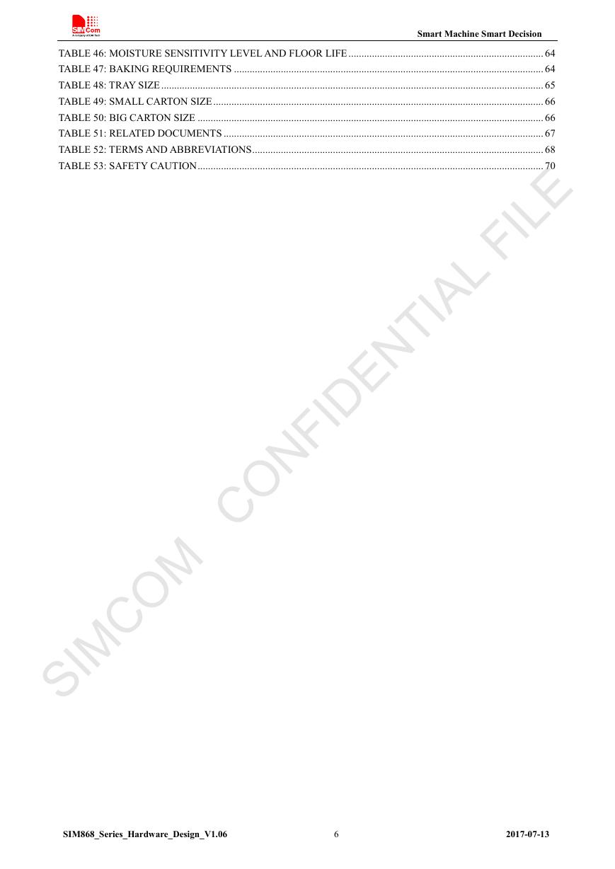
Smart Machine Smart Decision TABLE 46: MOISTURE SENSITIVITY LEVEL AND FLOOR LIFE ........................................................................... 64 TABLE 47: BAKING REQUIREMENTS ....................................................................................................................... 64 TABLE 48: TRAY SIZE ................................................................................................................................................... 65 TABLE 49: SMALL CARTON SIZE ............................................................................................................................... 66 TABLE 50: BIG CARTON SIZE ..................................................................................................................................... 66 TABLE 51: RELATED DOCUMENTS ........................................................................................................................... 67 TABLE 52: TERMS AND ABBREVIATIONS ................................................................................................................ 68 TABLE 53: SAFETY CAUTION ..................................................................................................................................... 70 SIM868_Series_Hardware_Design_V1.06 6 2017-07-13 SIMCOM CONFIDENTIAL FILE
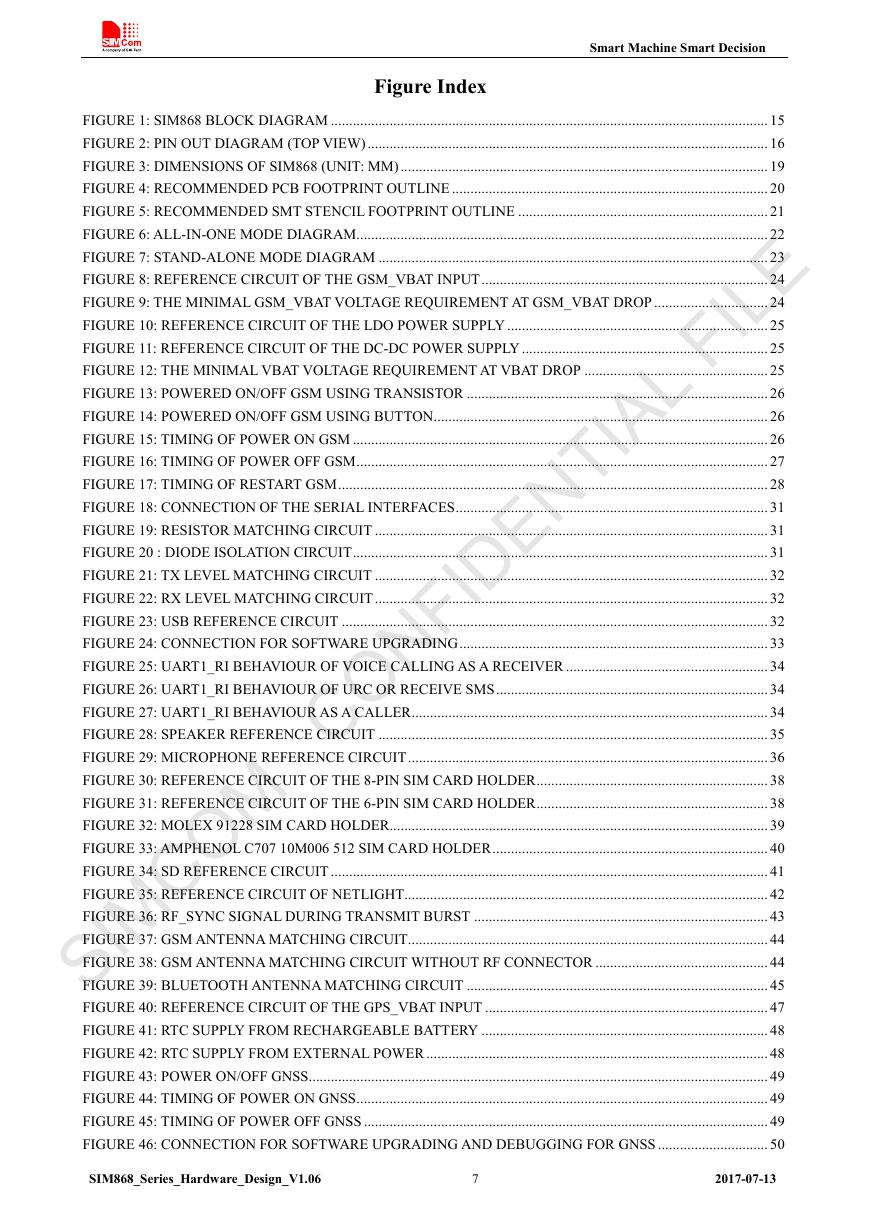
Smart Machine Smart Decision Figure Index FIGURE 1: SIM868 BLOCK DIAGRAM ....................................................................................................................... 15 FIGURE 2: PIN OUT DIAGRAM (TOP VIEW) ............................................................................................................. 16 FIGURE 3: DIMENSIONS OF SIM868 (UNIT: MM) .................................................................................................... 19 FIGURE 4: RECOMMENDED PCB FOOTPRINT OUTLINE ...................................................................................... 20 FIGURE 5: RECOMMENDED SMT STENCIL FOOTPRINT OUTLINE .................................................................... 21 FIGURE 6: ALL-IN-ONE MODE DIAGRAM................................................................................................................ 22 FIGURE 7: STAND-ALONE MODE DIAGRAM .......................................................................................................... 23 FIGURE 8: REFERENCE CIRCUIT OF THE GSM_VBAT INPUT .............................................................................. 24 FIGURE 9: THE MINIMAL GSM_VBAT VOLTAGE REQUIREMENT AT GSM_VBAT DROP ............................... 24 FIGURE 10: REFERENCE CIRCUIT OF THE LDO POWER SUPPLY ....................................................................... 25 FIGURE 11: REFERENCE CIRCUIT OF THE DC-DC POWER SUPPLY ................................................................... 25 FIGURE 12: THE MINIMAL VBAT VOLTAGE REQUIREMENT AT VBAT DROP .................................................. 25 FIGURE 13: POWERED ON/OFF GSM USING TRANSISTOR .................................................................................. 26 FIGURE 14: POWERED ON/OFF GSM USING BUTTON ........................................................................................... 26 FIGURE 15: TIMING OF POWER ON GSM ................................................................................................................. 26 FIGURE 16: TIMING OF POWER OFF GSM ................................................................................................................ 27 FIGURE 17: TIMING OF RESTART GSM ..................................................................................................................... 28 FIGURE 18: CONNECTION OF THE SERIAL INTERFACES ..................................................................................... 31 FIGURE 19: RESISTOR MATCHING CIRCUIT ........................................................................................................... 31 FIGURE 20 : DIODE ISOLATION CIRCUIT ................................................................................................................. 31 FIGURE 21: TX LEVEL MATCHING CIRCUIT ........................................................................................................... 32 FIGURE 22: RX LEVEL MATCHING CIRCUIT ........................................................................................................... 32 FIGURE 23: USB REFERENCE CIRCUIT .................................................................................................................... 32 FIGURE 24: CONNECTION FOR SOFTWARE UPGRADING .................................................................................... 33 FIGURE 25: UART1_RI BEHAVIOUR OF VOICE CALLING AS A RECEIVER ....................................................... 34 FIGURE 26: UART1_RI BEHAVIOUR OF URC OR RECEIVE SMS .......................................................................... 34 FIGURE 27: UART1_RI BEHAVIOUR AS A CALLER ................................................................................................. 34 FIGURE 28: SPEAKER REFERENCE CIRCUIT .......................................................................................................... 35 FIGURE 29: MICROPHONE REFERENCE CIRCUIT .................................................................................................. 36 FIGURE 30: REFERENCE CIRCUIT OF THE 8-PIN SIM CARD HOLDER ............................................................... 38 FIGURE 31: REFERENCE CIRCUIT OF THE 6-PIN SIM CARD HOLDER ............................................................... 38 FIGURE 32: MOLEX 91228 SIM CARD HOLDER....................................................................................................... 39 FIGURE 33: AMPHENOL C707 10M006 512 SIM CARD HOLDER ........................................................................... 40 FIGURE 34: SD REFERENCE CIRCUIT ....................................................................................................................... 41 FIGURE 35: REFERENCE CIRCUIT OF NETLIGHT................................................................................................... 42 FIGURE 36: RF_SYNC SIGNAL DURING TRANSMIT BURST ................................................................................ 43 FIGURE 37: GSM ANTENNA MATCHING CIRCUIT.................................................................................................. 44 FIGURE 38: GSM ANTENNA MATCHING CIRCUIT WITHOUT RF CONNECTOR ............................................... 44 FIGURE 39: BLUETOOTH ANTENNA MATCHING CIRCUIT .................................................................................. 45 FIGURE 40: REFERENCE CIRCUIT OF THE GPS_VBAT INPUT ............................................................................. 47 FIGURE 41: RTC SUPPLY FROM RECHARGEABLE BATTERY .............................................................................. 48 FIGURE 42: RTC SUPPLY FROM EXTERNAL POWER ............................................................................................. 48 FIGURE 43: POWER ON/OFF GNSS............................................................................................................................. 49 FIGURE 44: TIMING OF POWER ON GNSS ................................................................................................................ 49 FIGURE 45: TIMING OF POWER OFF GNSS .............................................................................................................. 49 FIGURE 46: CONNECTION FOR SOFTWARE UPGRADING AND DEBUGGING FOR GNSS .............................. 50 SIM868_Series_Hardware_Design_V1.06 7 2017-07-13 SIMCOM CONFIDENTIAL FILE
分享到:
收藏