Omni
ision ®
Advanced Information
Preliminary Datasheet
OV9656 Color CMOS SXGA (1.3 MegaPixel) CAMERACHIPTM Sensor
with OmniPixel® Technology
Applications
General Description
The OV9656 CAMERACHIP™ image sensor is a low
voltage CMOS device that provides the full functionality of
a single-chip SXGA (1280x1024) camera and image
processor in a small footprint package. The OV9656
provides full-frame, sub-sampled, scaled or windowed
8-bit/10-bit images in a wide range of formats, controlled
through the Serial Camera Control Bus (SCCB) interface.
This product has an image array capable of operating at
up to 15 frames per second (fps) in SXGA resolution with
complete user control over image quality, formatting and
output data transfer. All required image processing
functions, including exposure control, gamma, white
balance, color saturation, hue control, white pixel
canceling, noise canceling, and more, are also
programmable through the SCCB interface. In addition,
OmniVision CAMERACHIP sensors use proprietary sensor
technology to improve image quality by reducing or
eliminating common lighting/electrical sources of image
contamination, such as fixed pattern noise, smearing,
etc., to produce a clean, fully stable color image.
Pb
Note: The OV9656 uses a lead-free
package.
Features
High sensitivity for low-light operation
Low operating voltage for embedded portable apps
Standard SCCB interface
•
•
•
• Output support for Raw RGB, RGB (GRB 4:2:2,
RGB565/555), YUV (4:2:2) and YCbCr (4:2:2)
formats
Supports image sizes: SXGA, VGA, CIF, and any
size scaling down from CIF to 40x30
VarioPixel® method for sub-sampling
Automatic image control functions including
Automatic Exposure Control (AEC), Automatic Gain
Control (AGC), Automatic White Balance (AWB),
Automatic Band Filter (ABF), and Automatic
Black-Level Calibration (ABLC)
Image quality controls including color saturation,
gamma, sharpness (edge enhancement), lens
correction, white pixel canceling, noise canceling,
and 50/60 Hz luminance detection
Supports LED and flash strobe mode
Supports scaling
•
•
•
•
•
•
Ordering Information
Product
Package
OV09656-VL1A (Color, lead-free)
28-pin CSP2
•
•
•
•
Cellular and Picture Phones
Toys
PC Multimedia
Digital Still Cameras
Key Specifications
Power Supply
Power
Requirements
Temperature
Range
Active Array Size 1280 x 1024
Core 1.8VDC + 10%
Analog 2.45 to 3.0VDC
I/O 1.7V to 3.3Va
Active 90 mW typical
Standby <20 µA
Operation -30°C to 70°C
Stable Image 0°C to 50°C
(15fps SXGA YUV format)
Output Formats (8-bit)
• YUV/YCbCr 4:2:2
• RGB565/555
• GRB 4:2:2
• Raw RGB Data
Maximum
Image
Transfer Rate
Lens Size 1/4"
Chief Ray Angle 25° non linear
SXGA 15 fps
VGA, CIF and
down scaling 30 fps
Sensitivity 1.1 V/(Lux • sec)
S/N Ratio 42 dB
Dynamic Range 50 dB
Scan Mode Progressive
Maximum Exposure Interval 1050 x tROW
Gamma Correction Programmable
Pixel Size 3.18 µm x 3.18 µm
Dark Current 15 mV/s at 60°C
Well Capacity 10 K e
Fixed Pattern Noise <0.03% of VPEAK-TO-PEAK
Image Area 4.17 mm x 3.29 mm
Package Dimensions 5145 µm x 6145 µm
a.
I/O power should be 2.45V or higher when using the internal
regulator for Core (1.8V); otherwise, it is necessary to provide
an external 1.8V for the Core power supply.
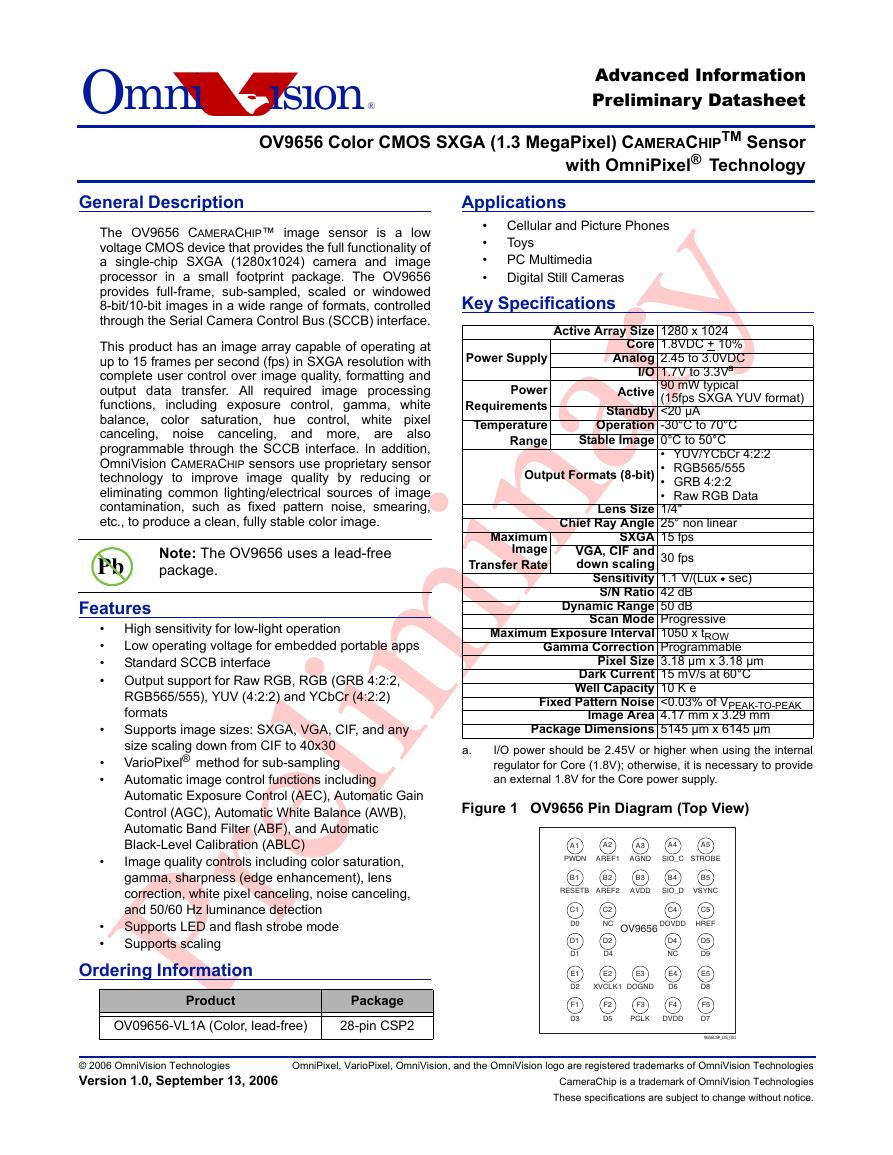
Figure 1 OV9656 Pin Diagram (Top View)
A1
A2
A3
A4
A5
PWDN AREF1
AGND
SIO_C
STROBE
B1
B2
B3
B4
B5
RESETB
AREF2
AVDD
SIO_D
VSYNC
C1
D0
D1
D1
E1
D2
F1
D3
C4
C5
DOVDD
HREF
OV9656
C2
NC
D2
D4
E2
F2
D5
D4
NC
E4
D6
F4
XVCLK1
DOGND
E3
F3
PCLK
DVDD
D5
D9
E5
D8
F5
D7
9656CSP_DS_001
© 2006 OmniVision Technologies
Version 1.0, September 13, 2006
OmniPixel, VarioPixel, OmniVision, and the OmniVision logo are registered trademarks of OmniVision Technologies
CameraChip is a trademark of OmniVision Technologies
These specifications are subject to change without notice.
�
OV9656
Color CMOS SXGA (1.3 MegaPixel) OmniPixel® CAMERACHIP™
Omni
ision
Functional Description
Image Sensor Array (1300 x 1028 active image array)
Analog Signal Processor
A/D Converters
Digital Signal Processor (DSP)
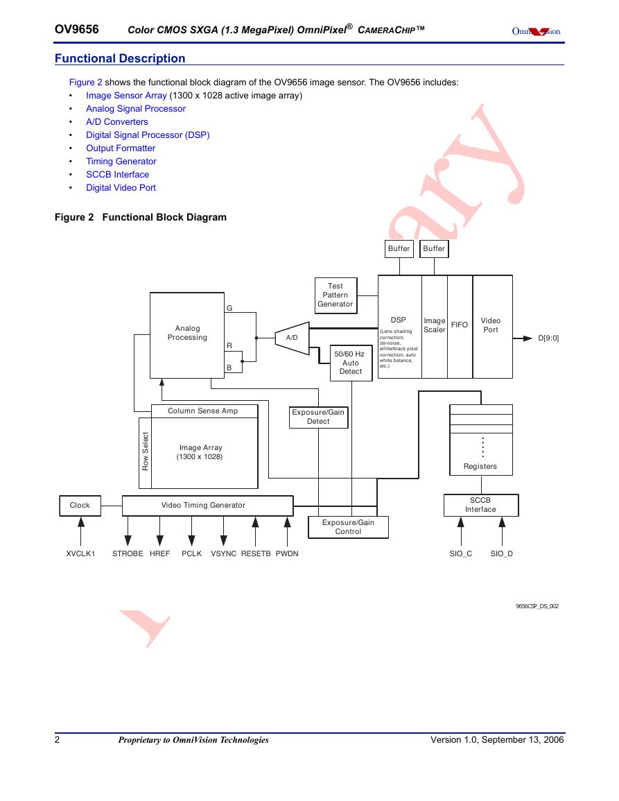
Figure 2 shows the functional block diagram of the OV9656 image sensor. The OV9656 includes:
•
•
•
•
• Output Formatter
Timing Generator
•
SCCB Interface
•
•
Digital Video Port
Figure 2 Functional Block Diagram
Buffer
Buffer
Analog
Processing
G
R
B
Test
Pattern
Generator
A/D
DSP
(Lens shading
correction,
de-noise,
white/black pixel
correction, auto
white balance,
etc.)
50/60 Hz
Auto
Detect
Image
Scaler
FIFO
Video
Port
D[9:0]
Column Sense Amp
Exposure/Gain
Detect
t
c
e
l
e
S
w
o
R
Image Array
(1300 x 1028)
Clock
Video Timing Generator
Exposure/Gain
Control
Registers
SCCB
Interface
XVCLK1
STROBE
HREF
PCLK
VSYNC
RESETB
PWDN
SIO_C
SIO_D
9656CSP_DS_002
2
Proprietary to OmniVision Technologies
Version 1.0, September 13, 2006
�
Omni
ision
Image Sensor Array
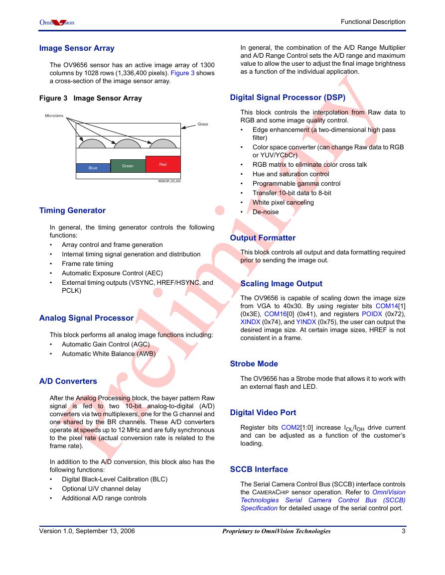
The OV9656 sensor has an active image array of 1300
columns by 1028 rows (1,336,400 pixels). Figure 3 shows
a cross-section of the image sensor array.
Functional Description
In general, the combination of the A/D Range Multiplier
and A/D Range Control sets the A/D range and maximum
value to allow the user to adjust the final image brightness
as a function of the individual application.
Figure 3 Image Sensor Array
Digital Signal Processor (DSP)
Microlens
Glass
Blue
Green
Red
9656CSP_DS_003
Timing Generator
In general, the timing generator controls the following
functions:
•
•
•
•
•
Array control and frame generation
Internal timing signal generation and distribution
Frame rate timing
Automatic Exposure Control (AEC)
External timing outputs (VSYNC, HREF/HSYNC, and
PCLK)
Analog Signal Processor
This block performs all analog image functions including:
•
•
Automatic Gain Control (AGC)
Automatic White Balance (AWB)
A/D Converters
is
to
fed
After the Analog Processing block, the bayer pattern Raw
signal
two 10-bit analog-to-digital (A/D)
converters via two multiplexers, one for the G channel and
one shared by the BR channels. These A/D converters
operate at speeds up to 12 MHz and are fully synchronous
to the pixel rate (actual conversion rate is related to the
frame rate).
In addition to the A/D conversion, this block also has the
following functions:
•
• Optional U/V channel delay
•
Digital Black-Level Calibration (BLC)
Additional A/D range controls
•
This block controls the interpolation from Raw data to
RGB and some image quality control.
•
Edge enhancement (a two-dimensional high pass
filter)
Color space converter (can change Raw data to RGB
or YUV/YCbCr)
RGB matrix to eliminate color cross talk
Hue and saturation control
Programmable gamma control
Transfer 10-bit data to 8-bit
•
•
•
•
• White pixel canceling
•
De-noise
Output Formatter
This block controls all output and data formatting required
prior to sending the image out.
Scaling Image Output
The OV9656 is capable of scaling down the image size
from VGA to 40x30. By using register bits COM14[1]
(0x3E), COM16[0] (0x41), and registers POIDX (0x72),
XINDX (0x74), and YINDX (0x75), the user can output the
desired image size. At certain image sizes, HREF is not
consistent in a frame.
Strobe Mode
The OV9656 has a Strobe mode that allows it to work with
an external flash and LED.
Digital Video Port
Register bits COM2[1:0] increase IOL/IOH drive current
and can be adjusted as a function of the customer’s
loading.
SCCB Interface
The Serial Camera Control Bus (SCCB) interface controls
the CAMERACHIP sensor operation. Refer to OmniVision
Technologies Serial Camera Control Bus
(SCCB)
Specification for detailed usage of the serial control port.
Version 1.0, September 13, 2006
Proprietary to OmniVision Technologies
3
�
OV9656
Color CMOS SXGA (1.3 MegaPixel) OmniPixel® CAMERACHIP™
Omni
ision
Pin Description
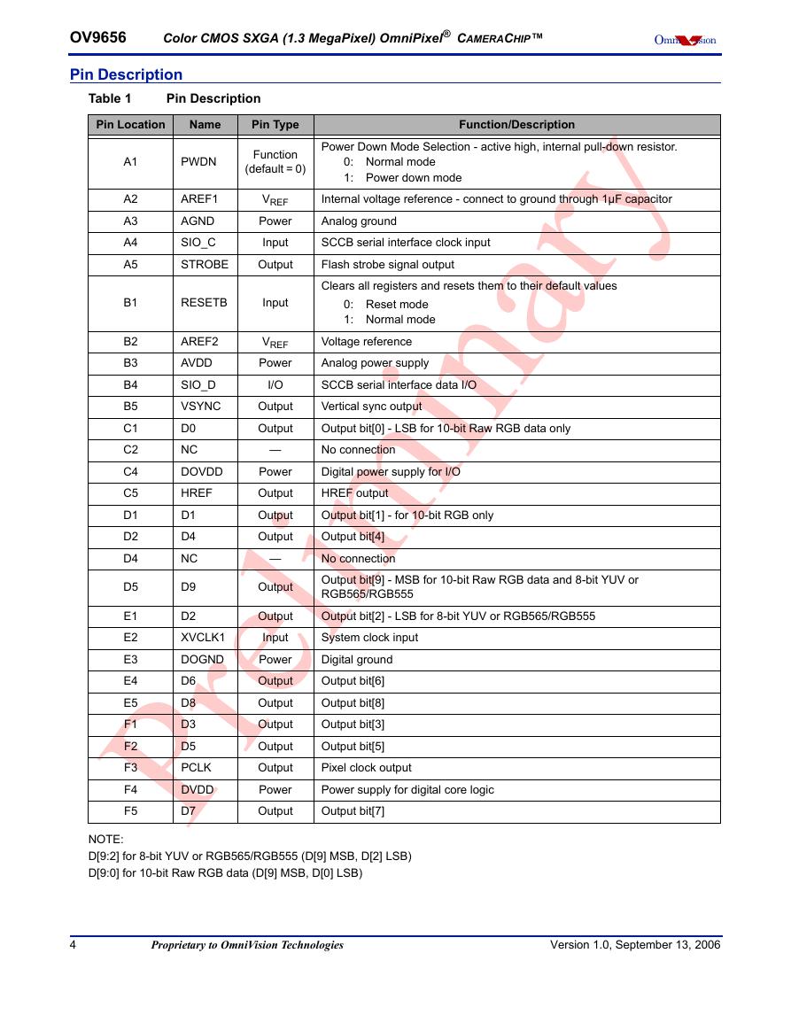
Table 1
Pin Description
Pin Location
Name
Pin Type
Function/Description
A1
A2
A3
A4
A5
B1
B2
B3
B4
B5
C1
C2
C4
C5
D1
D2
D4
D5
E1
E2
E3
E4
E5
F1
F2
F3
F4
F5
PWDN
AREF1
AGND
SIO_C
STROBE
Function
(default = 0)
VREF
Power
Input
Output
RESETB
Input
AREF2
AVDD
SIO_D
VSYNC
D0
NC
DOVDD
HREF
D1
D4
NC
D9
D2
XVCLK1
DOGND
D6
D8
D3
D5
PCLK
DVDD
D7
VREF
Power
I/O
Output
Output
—
Power
Output
Output
Output
—
Output
Output
Input
Power
Output
Output
Output
Output
Output
Power
Output
Power Down Mode Selection - active high, internal pull-down resistor.
0: Normal mode
1: Power down mode
Internal voltage reference - connect to ground through 1µF capacitor
Analog ground
SCCB serial interface clock input
Flash strobe signal output
Clears all registers and resets them to their default values
0: Reset mode
1: Normal mode
Voltage reference
Analog power supply
SCCB serial interface data I/O
Vertical sync output
Output bit[0] - LSB for 10-bit Raw RGB data only
No connection
Digital power supply for I/O
HREF output
Output bit[1] - for 10-bit RGB only
Output bit[4]
No connection
Output bit[9] - MSB for 10-bit Raw RGB data and 8-bit YUV or
RGB565/RGB555
Output bit[2] - LSB for 8-bit YUV or RGB565/RGB555
System clock input
Digital ground
Output bit[6]
Output bit[8]
Output bit[3]
Output bit[5]
Pixel clock output
Power supply for digital core logic
Output bit[7]
NOTE:
D[9:2] for 8-bit YUV or RGB565/RGB555 (D[9] MSB, D[2] LSB)
D[9:0] for 10-bit Raw RGB data (D[9] MSB, D[0] LSB)
4
Proprietary to OmniVision Technologies
Version 1.0, September 13, 2006
�
Omni
ision
Electrical Characteristics
Electrical Characteristics
Table 2
Ambient Storage Temperature
Absolute Maximum Ratings
Supply Voltages (with respect to Ground)
-40ºC to +95ºC
VDD-A
VDD-C
VDD-IO
4.5 V
3 V
3 V
All Input/Output Voltages (with respect to Ground)
Lead-free Temperature, Surface-mount process
-0.3V to VDD-IO+0.5V
245ºC
NOTE: Exceeding the Absolute Maximum ratings shown above invalidates all AC and DC electrical specifications and may
result in permanent device damage.
Table 3
DC Characteristics (-30°C < TA < 70°C)
Symbol
Parameter
Condition
Standby Current
DC supply voltage – Core
Active (Operating) Current
DC supply voltage – Analog
DC supply voltage – I/O power
VDD-A
VDD-C
VDD-IO
IDDA
IDDS-SCCB
IDDS-PWDN Standby Current
VIH
VIL
VOH
VOL
IOH
IOL
IL
a. VDD-A = 2.5V, VDD-C = 1.8V, VDD-IO = 2.5V
Input voltage HIGH
Input voltage LOW
Input/Output Leakage
Output voltage HIGH
Output voltage LOW
Output current HIGH
Output current LOW
Max
3.0
1.98
3.3
0.3 x VDD-IO
0.1 x VDD-IO
± 1
Unit
V
V
V
mA
mA
µA
V
V
V
V
mA
mA
µA
–
–
–
See Note a
See Note b
Min
2.45
1.62
1.7
Typ
2.5
1.8
–
20
1
10
CMOS
0.7 x VDD-IO
CMOS
0.9 x VDD-IO
See Note c
GND to VDD-IO
8
15
IDDA = ∑{IDD-IO+ IDD-C + IDD-A}, fCLK = 24MHz at 7.5 fps YUV output, no I/O loading
b. VDD-A = 2.5V, VDD-C = 1.8V, VDD-IO = 2.5V
IDDS-SCCB refers to a SCCB-initiated Standby, while IDDS-PWDN refers to a PWDN pin-initiated Standby
Standard Output Loading = 25pF, 1.2KΩ
c.
Version 1.0, September 13, 2006
Proprietary to OmniVision Technologies
5
�
OV9656
Color CMOS SXGA (1.3 MegaPixel) OmniPixel® CAMERACHIP™
Omni
ision
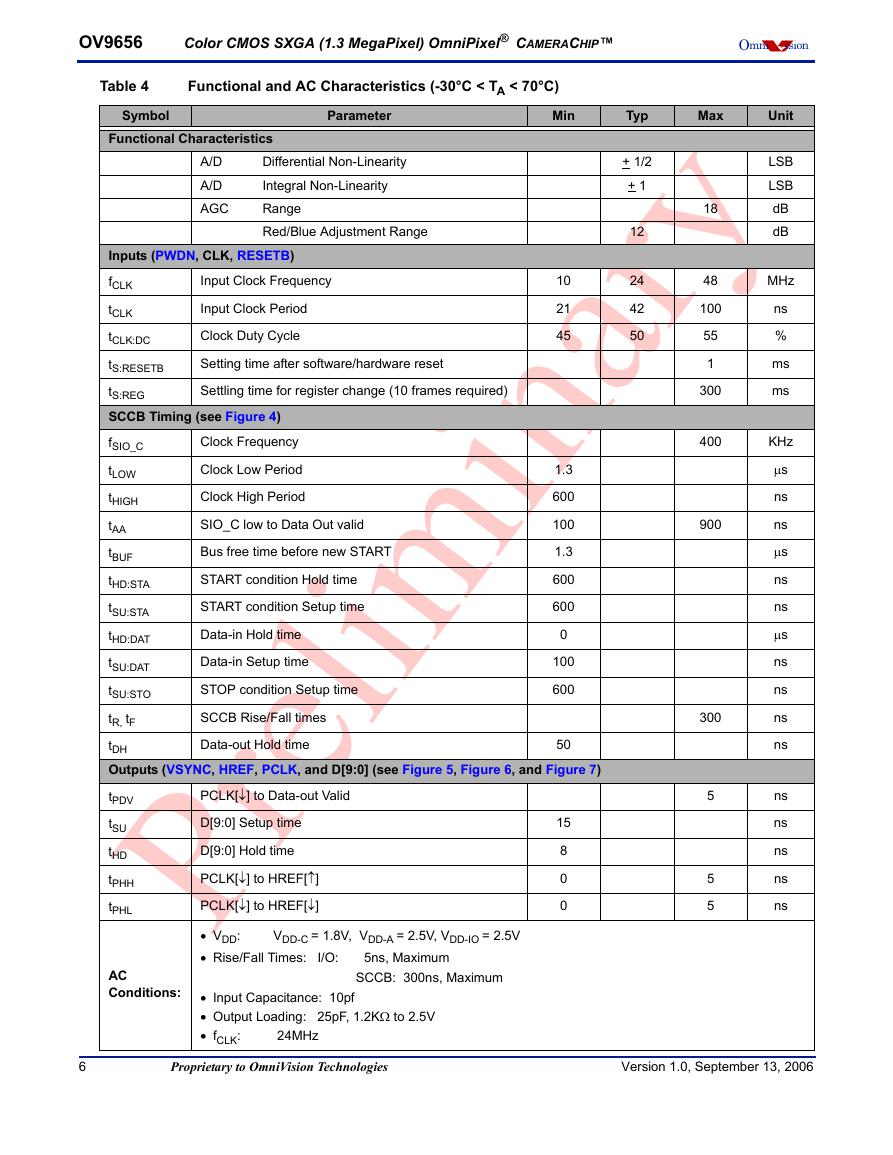
Table 4
Functional and AC Characteristics (-30°C < TA < 70°C)
Symbol
Parameter
Min
Typ
Max
Functional Characteristics
Unit
LSB
LSB
dB
dB
MHz
ns
%
ms
ms
KHz
μs
ns
ns
μs
ns
ns
μs
ns
ns
ns
ns
ns
ns
ns
ns
ns
A/D
A/D
AGC
Differential Non-Linearity
Integral Non-Linearity
Range
Red/Blue Adjustment Range
Clock High Period
10
21
45
0
100
600
Input Clock Period
Clock Duty Cycle
Clock Frequency
Clock Low Period
Input Clock Frequency
SIO_C low to Data Out valid
Bus free time before new START
Setting time after software/hardware reset
Settling time for register change (10 frames required)
Inputs (PWDN, CLK, RESETB)
fCLK
tCLK
tCLK:DC
tS:RESETB
tS:REG
SCCB Timing (see Figure 4)
fSIO_C
tLOW
tHIGH
tAA
tBUF
tHD:STA
tSU:STA
tHD:DAT
tSU:DAT
tSU:STO
tR, tF
tDH
Outputs (VSYNC, HREF, PCLK, and D[9:0] (see Figure 5, Figure 6, and Figure 7)
tPDV
tSU
tHD
tPHH
tPHL
START condition Setup time
STOP condition Setup time
START condition Hold time
PCLK[↓] to Data-out Valid
SCCB Rise/Fall times
PCLK[↓] to HREF[↓]
1.3
600
100
1.3
600
600
PCLK[↓] to HREF[↑]
Data-out Hold time
50
15
8
0
0
D[9:0] Setup time
D[9:0] Hold time
Data-in Hold time
Data-in Setup time
+ 1/2
+ 1
12
24
42
50
18
48
100
55
1
300
400
900
300
5
5
5
AC
Conditions:
• VDD: VDD-C = 1.8V, VDD-A = 2.5V, VDD-IO = 2.5V
• Rise/Fall Times: I/O: 5ns, Maximum
SCCB: 300ns, Maximum
• Input Capacitance: 10pf
• Output Loading: 25pF, 1.2KΩ to 2.5V
• fCLK: 24MHz
6
Proprietary to OmniVision Technologies
Version 1.0, September 13, 2006
�
Omni
ision
Timing Specifications
Timing Specifications
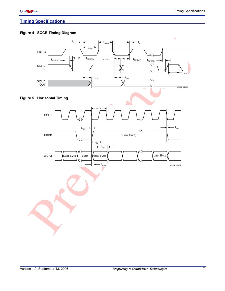
Figure 4 SCCB Timing Diagram
tF
tHIGH
tR
tLOW
tSU:STA
tHD:STA
tHD:DAT
tSU:DAT
tSU:STO
tAA
tDH
SIO_C
SIO_D
IN
SIO_D
OUT
Figure 5 Horizontal Timing
PCLK
HREF
tPHL
tPCLK
tSU
tHD
(Row Data)
tBUF
9656CSP_DS_004
tPHL
D[9:0]
Last Byte
Zero
First Byte
Last Byte
tPDV
9656CSP_DS_005
Version 1.0, September 13, 2006
Proprietary to OmniVision Technologies
7
�
OV9656
Color CMOS SXGA (1.3 MegaPixel) OmniPixel® CAMERACHIP™
Omni
ision
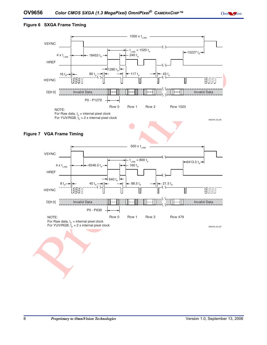
Figure 6 SXGA Frame Timing
4 x tLINE
18453 tP
1050 x tLINE
tLINE = 1520 tP
240 tP
15227 tP
16 tP
80 tP
1280 tP
117 tP
43 tP
VSYNC
HREF
HSYNC
D[9:0]
Invalid Data
Invalid Data
P0 - P1279
NOTE:
For Raw data, tP = internal pixel clock
For YUV/RGB, tP = 2 x internal pixel clock
Row 0
Row 1
Row 2
Row 1023
9656CSP_DS_006
Figure 7 VGA Frame Timing
4 x tLINE
6546.5 tP
500 x tLINE
tLINE = 800 tP
160 tP
6413.5 tP
8 tP
40 tP
640 tP
98.5 tP
21.5 tP
VSYNC
HREF
HSYNC
D[9:0]
Invalid Data
Invalid Data
P0 - P639
NOTE:
For Raw data, tP = internal pixel clock
For YUV/RGB, tP = 2 x internal pixel clock
Row 0
Row 1
Row 2
Row 479
9656CSP_DS_007
8
Proprietary to OmniVision Technologies
Version 1.0, September 13, 2006
�



 V2版本原理图(Capacitive-Fingerprint-Reader-Schematic_V2).pdf
 摄像头工作原理.doc
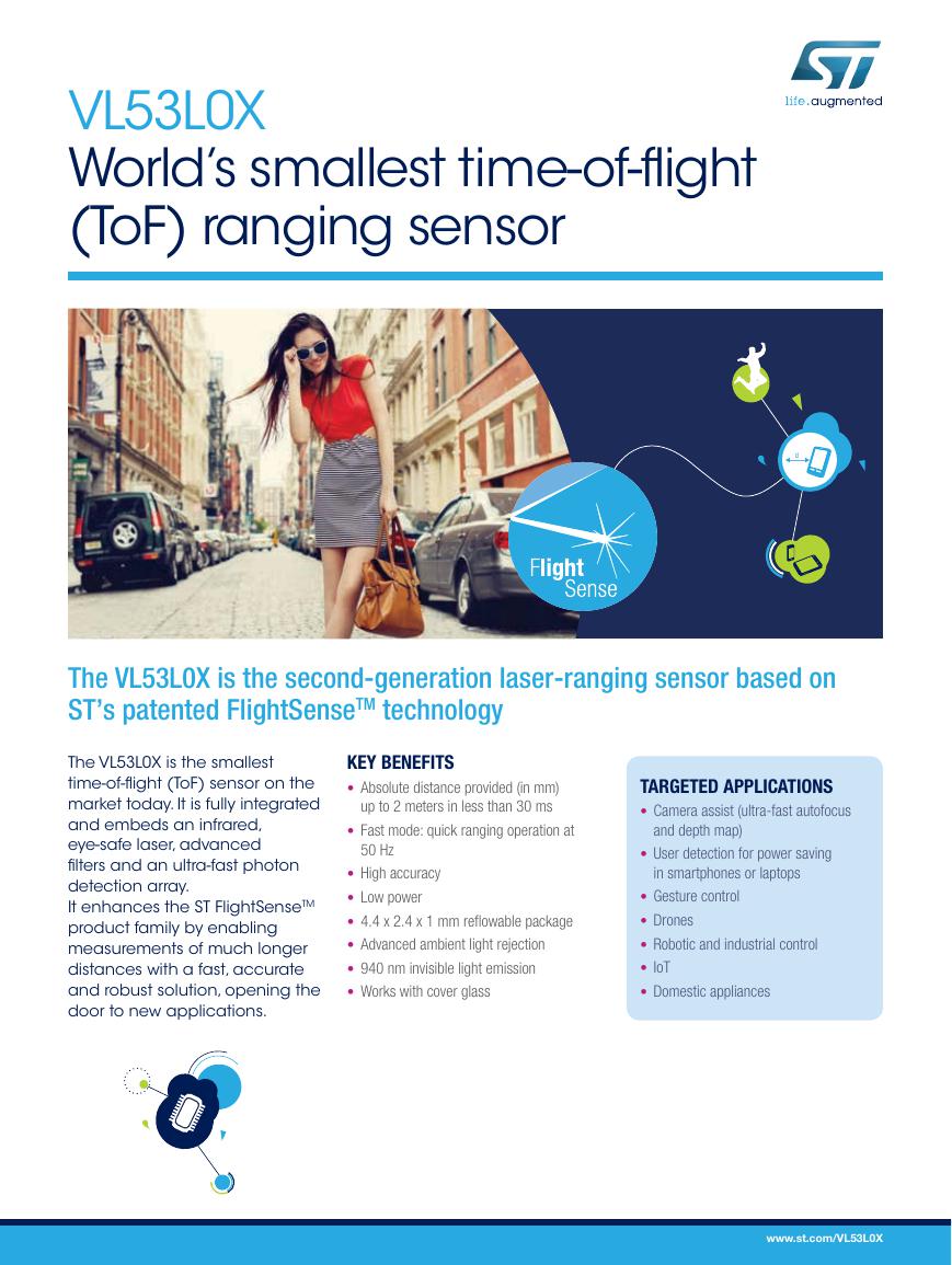 VL53L0X简要说明(En.FLVL53L00216).pdf
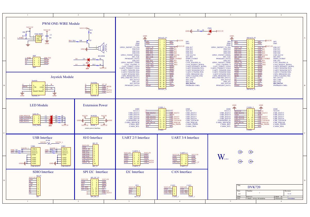 原理图(DVK720-Schematic).pdf
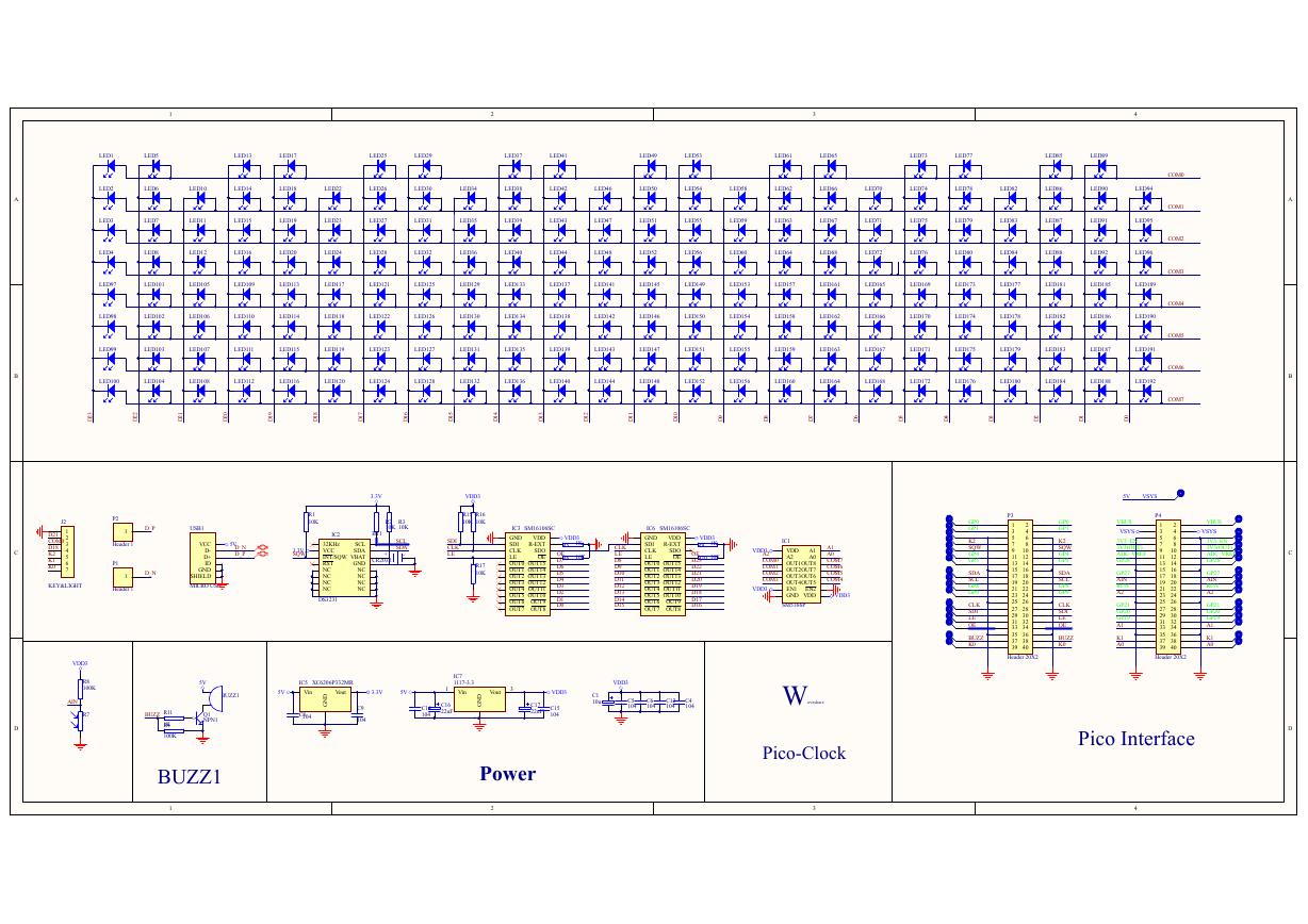 原理图(Pico-Clock-Green-Schdoc).pdf
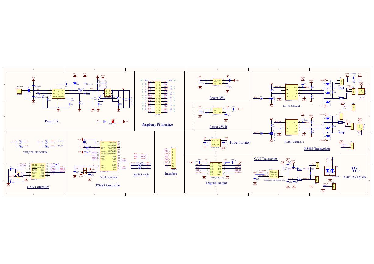 原理图(RS485-CAN-HAT-B-schematic).pdf
 File:SIM7500_SIM7600_SIM7800 Series_SSL_Application Note_V2.00.pdf
 ADS1263(Ads1262).pdf
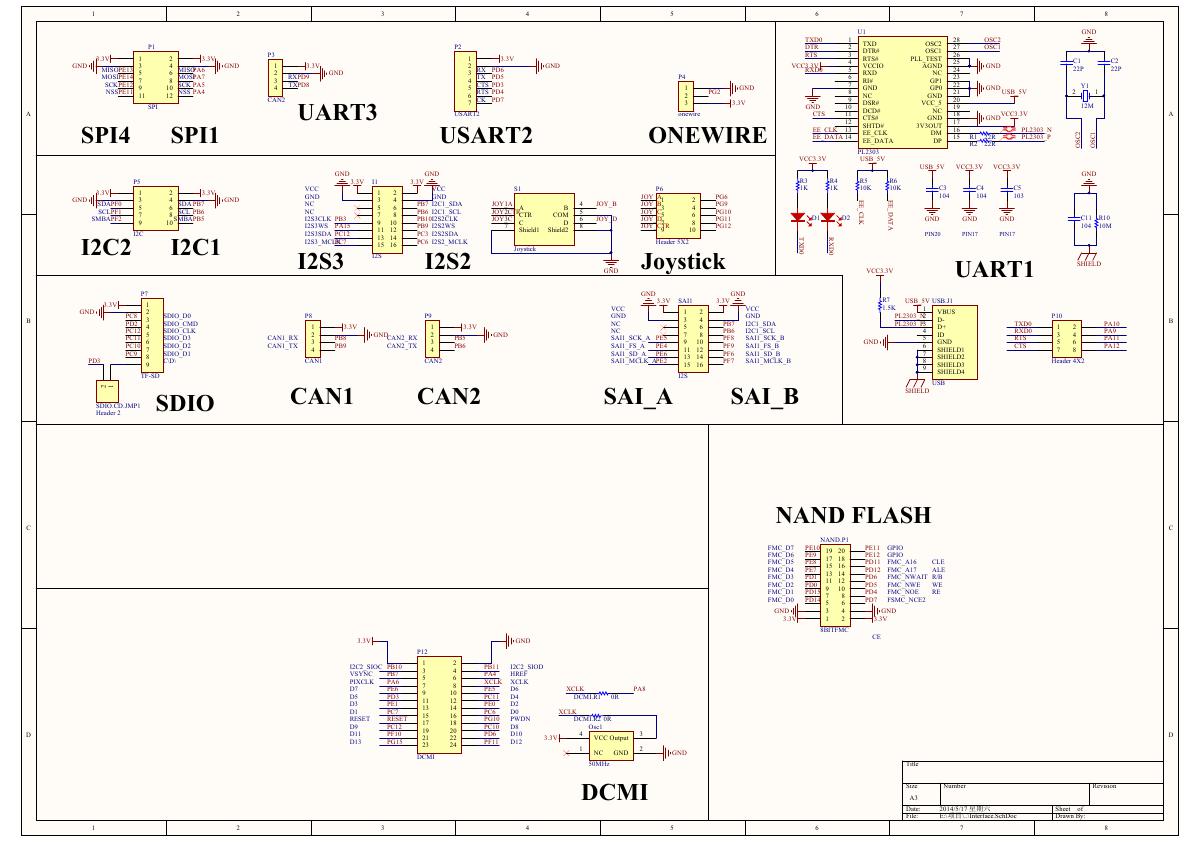 原理图(Open429Z-D-Schematic).pdf
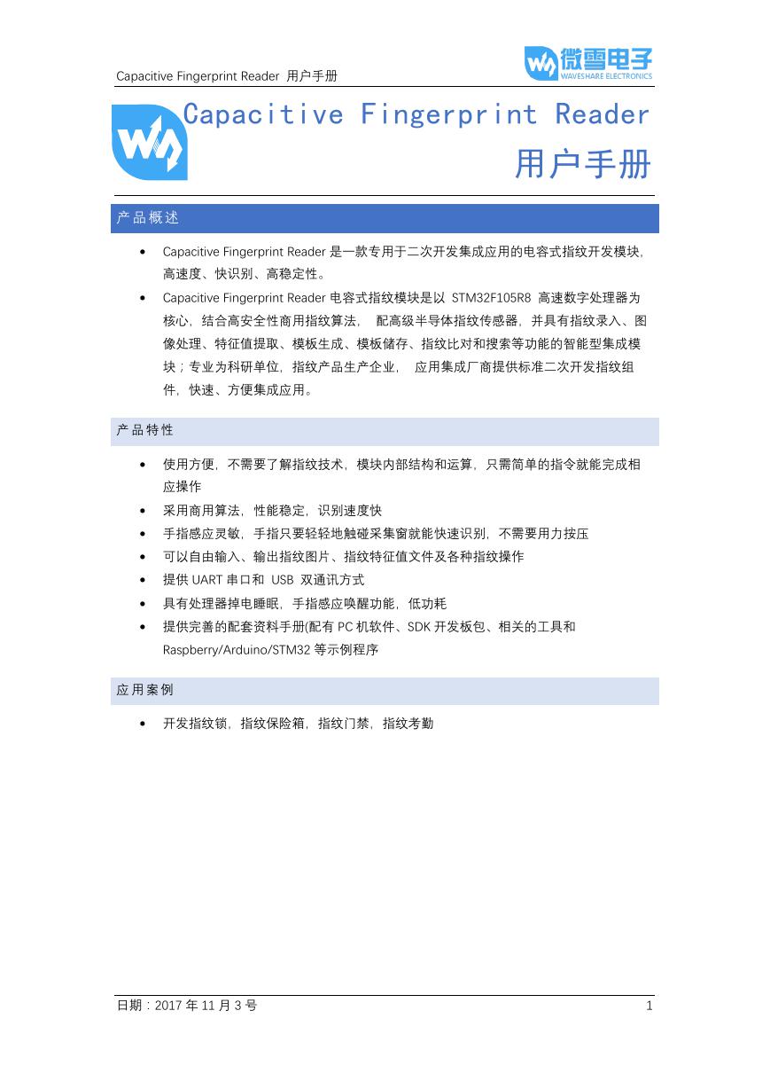 用户手册(Capacitive_Fingerprint_Reader_User_Manual_CN).pdf
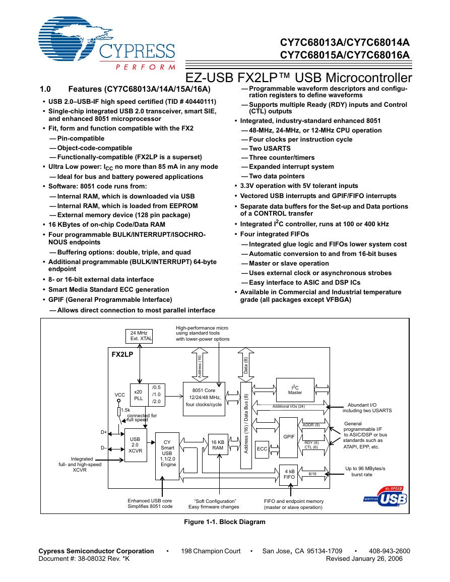 CY7C68013A(英文版)(CY7C68013A).pdf
 TechnicalReference_Dem.pdf