AW9523B
July 2019 V1.5
16 MULTI-FUNCTION LED DRIVER AND GPIO
CONTROLLER WITH I2C INTERFACE
GENERAL DESCRIPTION
AW9523B is a 16 multi-function LED driver and
GPIO controller. Any of the 16 I/O ports can be
configured as LED drive mode or GPIO mode.
Furthermore, any GPIO can be configured as an
input or an output independently.
After power on, all the 16 I/O ports are configured
as GPIO output as default, which default states are
set according to the I2C device address selection
inputs, AD0 and AD1. All I/O ports configured as
inputs are continuously monitored
for state
changes. State changes are indicated by the INTN
output. When AW9523B reads GPIO state through
the I2C interface, the interrupt is cleared. Interrupt
has 8μs deglitch.
When the I/O ports are configured as LED drive
mode, AW9523B can set the current of LED drive
between 0~IMAX by I2C interface, which is divided
by 256 steps linear dimming. The default maximum
current (IMAX) is 37mA, and IMAX can be changed
in GCR register.
AW9523B is available in QFN4mm×4mm×0.75mm
-24L package, and 2.5V~5.5V power supply.
FEATURES
16 multi-function I/O, each for LED drive
(current-source dimming) or GPIO mode
256 steps linear dimming in LED drive mode
Any GPIO can be configured as an input or an
output independently
Support interrupt, 8μs deglitch, low-level active
Standard I2C interface, AD1/AD0 select I2C
device address
SDA, SCL, RSTN, and all GPIO can accept in
1.8V logic input
Supply shutdown function, low-level active
2.5V~5.5V power supply
APPLICATIONS
Cell Phone
PDA/MP3/MP4/CD/Mini display
www.awinic.com.cn 1 Copyright © 2014 SHANGHAI AWINIC TECHNOLOGY CO., LTD
�
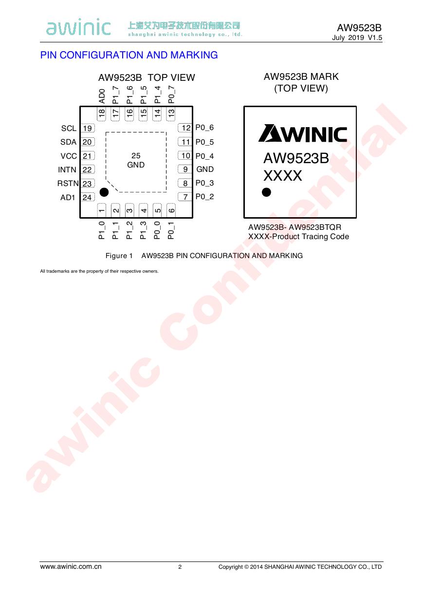
PIN CONFIGURATION AND MARKING
AW9523B
July 2019 V1.5
Figure 1 AW9523B PIN CONFIGURATION AND MARKING
All trademarks are the property of their respective owners.
www.awinic.com.cn 2 Copyright © 2014 SHANGHAI AWINIC TECHNOLOGY CO., LTD
P1_0123456P1_1P1_2P1_3P0_0P0_1131415161718192021222324P0_2P0_3GNDP0_4P0_5P0_6P0_7P1_4P1_5P1_6P1_7AD0SCLSDAVCCINTNRSTNAD1AW9523BXXXXAW9523B- AW9523BTQRXXXX-Product Tracing CodeAW9523B 78101112TOP VIEW25GND9AW9523B MARK(TOP VIEW)�
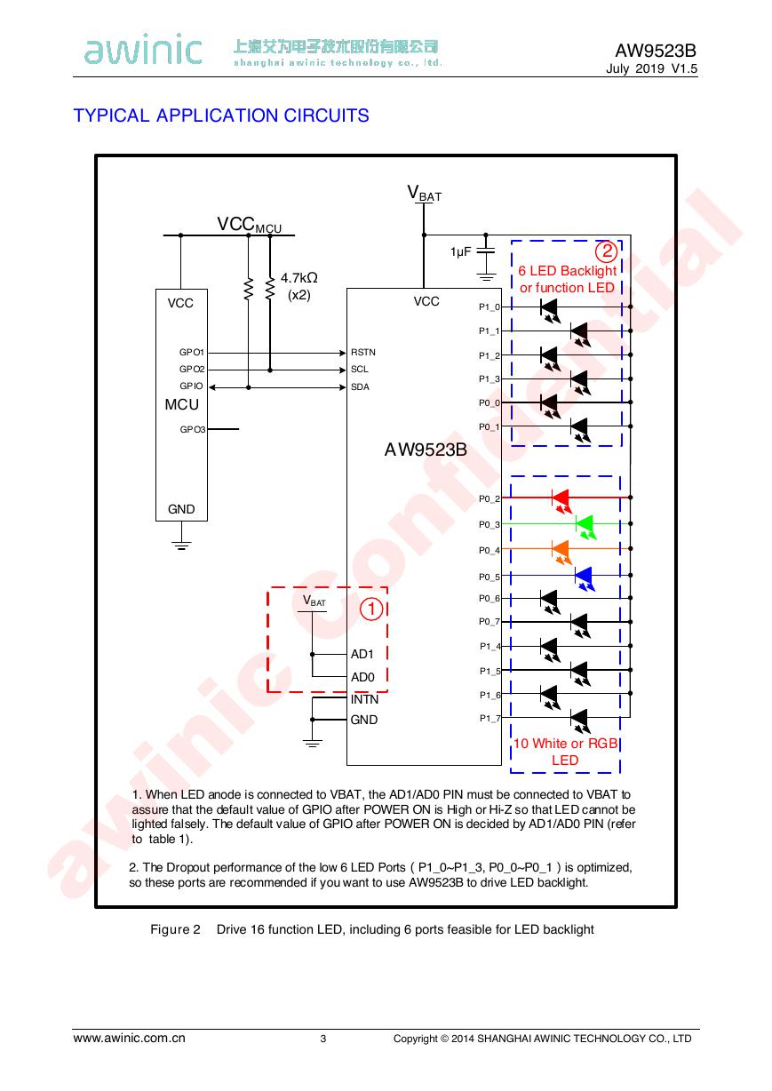
TYPICAL APPLICATION CIRCUITS
AW9523B
July 2019 V1.5
Figure 2 Drive 16 function LED, including 6 ports feasible for LED backlight
www.awinic.com.cn 3 Copyright © 2014 SHANGHAI AWINIC TECHNOLOGY CO., LTD
VCCRSTNP1_0VCCMCUSCLSDA4.7kΩ(x2)MCUVCCP1_1P1_2AW9523BP1_3P0_0P0_1P0_2P0_3P0_4P0_5P0_6P0_7GND1μFP1_4P1_5P1_6P1_7GPO1GPO2GPIOGPO3VBAT6 LED Backlight or function LED10 White or RGB LEDGNDINTNAD1AD01VBAT22. The Dropout performance of the low 6 LED Ports(P1_0~P1_3, P0_0~P0_1)is optimized, so these ports are recommended if you want to use AW9523B to drive LED backlight.1. When LED anode is connected to VBAT, the AD1/AD0 PIN must be connected to VBAT to assure that the default value of GPIO after POWER ON is High or Hi-Z so that LED cannot be lighted falsely. The default value of GPIO after POWER ON is decided by AD1/AD0 PIN (refer to table 1).�
AW9523B
July 2019 V1.5
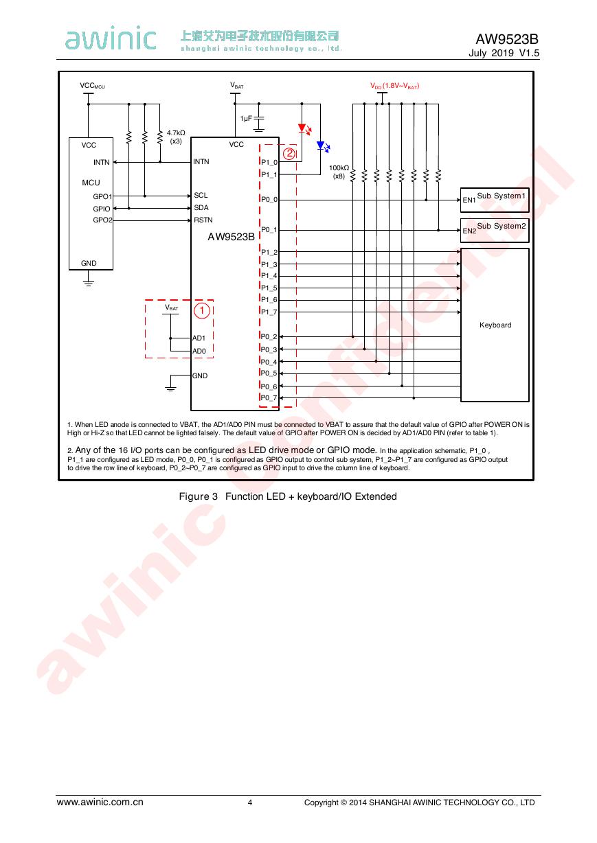
Figure 3 Function LED + keyboard/IO Extended
www.awinic.com.cn 4 Copyright © 2014 SHANGHAI AWINIC TECHNOLOGY CO., LTD
VCCVBATSCLP1_0VCCMCUSDARSTN4.7kΩ(x3)INTNVCCP0_1P0_2P0_3P1_1P0_0P1_4P1_5P1_6P1_7P0_4P0_5P0_6P0_7GND1μFKeyboardSub System1EN1100kΩ(x8)MCUINTNGPO1GPIOGPO2VDD (1.8V~VBAT)P1_3P1_22. Any of the 16 I/O ports can be configured as LED drive mode or GPIO mode. In the application schematic, P1_0,P1_1 are configured as LED mode, P0_0, P0_1 is configured as GPIO output to control sub system, P1_2~P1_7 are configured as GPIO output to drive the row line of keyboard, P0_2~P0_7 are configured as GPIO input to drive the column line of keyboard.AW9523BGNDAD1AD01VBAT21. When LED anode is connected to VBAT, the AD1/AD0 PIN must be connected to VBAT to assure that the default value of GPIO after POWER ON is High or Hi-Z so that LED cannot be lighted falsely. The default value of GPIO after POWER ON is decided by AD1/AD0 PIN (refer to table 1).Sub System2EN2�
AW9523B
July 2019 V1.5
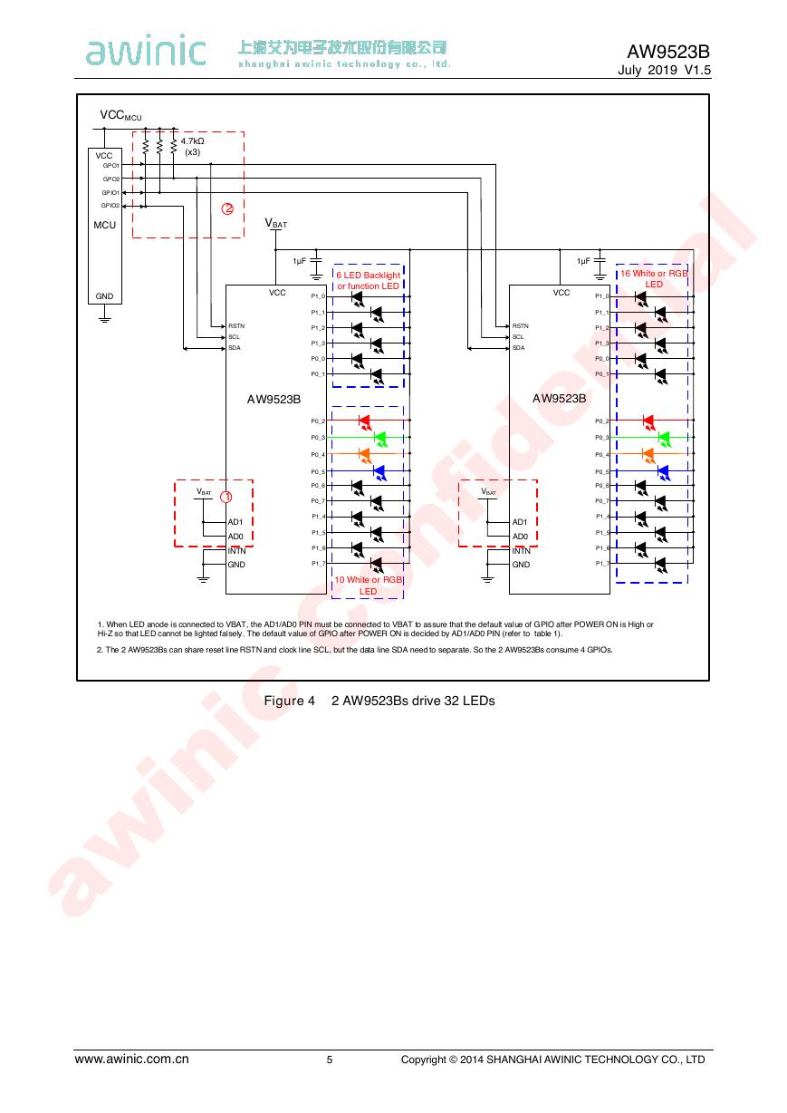
Figure 4 2 AW9523Bs drive 32 LEDs
www.awinic.com.cn 5 Copyright © 2014 SHANGHAI AWINIC TECHNOLOGY CO., LTD
VCCRSTNP1_0VCCMCUSCLSDA4.7kΩ(x3)MCUVCCP1_1P1_2AW9523BP1_3P0_0P0_1P0_2P0_3P0_4P0_5P0_6P0_7GND1μFP1_4P1_5P1_6P1_7GPO1GPO2GPIO2GPIO1GNDINTNAD1AD0VBAT2. The 2 AW9523Bs can share reset line RSTN and clock line SCL, but the data line SDA need to separate. So the 2 AW9523Bs consume 4 GPIOs.VCCRSTNP1_0SCLSDAP1_1P1_2AW9523BP1_3P0_0P0_1P0_2P0_3P0_4P0_5P0_6P0_71μFP1_4P1_5P1_6P1_7VBATGNDINTNAD1AD0VBAT121. When LED anode is connected to VBAT, the AD1/AD0 PIN must be connected to VBAT to assure that the default value of GPIO after POWER ON is High or Hi-Z so that LED cannot be lighted falsely. The default value of GPIO after POWER ON is decided by AD1/AD0 PIN (refer to table 1).6 LED Backlight or function LED10 White or RGB LED16 White or RGB LED�
PIN DEFINITION
Pin No.
Name
Description
AW9523B
July 2019 V1.5
GPIO mode default, input or output, push-pull mode. Can be configured as LED drive mode. The default
state after power on is related to AD1/AD0 PIN.
GPIO mode default, input or output, push-pull mode. Can be configured as LED drive mode. The default
state after power on is related to AD1/AD0 PIN.
GPIO mode default, input or output, push-pull mode. Can be configured as LED drive mode. The default
state after power on is related to AD1/AD0 PIN.
GPIO mode default, input or output, push-pull mode. Can be configured as LED drive mode. The default
state after power on is related to AD1/AD0 PIN.
GPIO mode default, input or output, open-drain (default) or push-pull mode. Can be configured as LED
drive mode. The default state after power on is related to AD1/AD0 PIN.
GPIO mode default, input or output, open-drain (default) or push-pull mode. Can be configured as LED
drive mode. The default state after power on is related to AD1/AD0 PIN.
GPIO mode default, input or output, open-drain (default) or push-pull mode. Can be configured as LED
drive mode. The default state after power on is related to AD1/AD0 PIN.
GPIO mode default, input or output, open-drain (default) or push-pull mode. Can be configured as LED
drive mode. The default state after power on is related to AD1/AD0 PIN.
GND
Ground supply
GPIO mode default, input or output, open-drain (default) or push-pull mode. Can be configured as LED
drive mode. The default state after power on is related to AD1/AD0 PIN.
GPIO mode default, input or output, open-drain (default) or push-pull mode. Can be configured as LED
drive mode. The default state after power on is related to AD1/AD0 PIN.
GPIO mode default, input or output, open-drain (default) or push-pull mode. Can be configured as LED
drive mode. The default state after power on is related to AD1/AD0 PIN.
GPIO mode default, input or output, open-drain (default) or push-pull mode. Can be configured as LED
drive mode. The default state after power on is related to AD1/AD0 PIN.
GPIO mode default, input or output, push-pull mode. Can be configured as LED drive mode. The default
state after power on is related to AD1/AD0 PIN.
GPIO mode default, input or output, push-pull mode. Can be configured as LED drive mode. The default
state after power on is related to AD1/AD0 PIN.
GPIO mode default, input or output, push-pull mode. Can be configured as LED drive mode. The default
state after power on is related to AD1/AD0 PIN.
GPIO mode default, input or output, push-pull mode. Can be configured as LED drive mode. The default
state after power on is related to AD1/AD0 PIN.
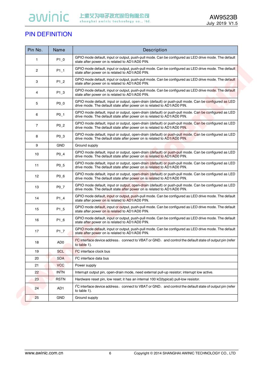
I2C interface device address,connect to VBAT or GND,and control the default state of output pin (refer
to table 1).
INTN
Interrupt output pin, open-drain mode, need external pull-up resistor; interrupt low active.
Hardware reset pin, low reset; it has an internal 100 kΩ(typical) pull-low resistor.
I2C interface device address,connect to VBAT or GND,and control the default state of output pin (refer
to table 1).
P1_0
P1_1
P1_2
P1_3
P0_0
P0_1
P0_2
P0_3
P0_4
P0_5
P0_6
P0_7
1
2
3
4
5
6
7
8
9
10
11
12
13
14
15
16
17
18
19
20
21
22
23
24
P1_7
P1_6
P1_5
P1_4
I2C interface clock bus
I2C interface data bus
Power supply
RSTN
SCL
SDA
VCC
AD0
AD1
25
GND
Ground supply
www.awinic.com.cn 6 Copyright © 2014 SHANGHAI AWINIC TECHNOLOGY CO., LTD
�
ORDERING INFORMATION
AW9523B
July 2019 V1.5
Part Number
Temperature
Package
Marking
Moisture
Sensitivity
Level
Environmental
Delivery
Information
Form
AW9523BTQR
-40℃~125℃
4mm×4mm
TQFN-24L
AW9523B
MSL3
RoHS+HF
Reel
6000 units/
Tape and
RANGE
-0.3V to 6 V
-0.3V to VCC
3.2 W
31℃/W
150℃
-65°C to 150°C
260°C
±2kV
+IT:200mA
-IT:-200mA
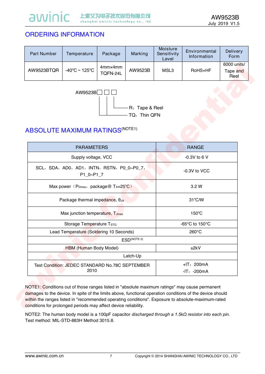
ABSOLUTE MAXIMUM RATINGS(NOTE1)
PARAMETERS
Supply voltage, VCC
SCL,SDA,AD0,AD1,INTN,RSTN,P0_0~P0_7,
P1_0~P1_7
Max power(PDmax,package@ TA=25℃)
Lead Temperature (Soldering 10 Seconds)
Package thermal impedance, θJA
Max junction temperature, TJmax
Storage Temperature TSTG
2010
HBM (Human Body Model)
ESD(NOTE 2)
Latch-Up
Test Condition: JEDEC STANDARD No.78C SEPTEMBER
NOTE1: Conditions out of those ranges listed in "absolute maximum ratings" may cause permanent
damages to the device. In spite of the limits above, functional operation conditions of the device should
within the ranges listed in "recommended operating conditions". Exposure to absolute-maximum-rated
conditions for prolonged periods may affect device reliability.
NOTE2: The human body model is a 100pF capacitor discharged through a 1.5kΩ resistor into each pin.
Test method: MIL-STD-883H Method 3015.8.
www.awinic.com.cn 7 Copyright © 2014 SHANGHAI AWINIC TECHNOLOGY CO., LTD
AW9523BR:Tape & ReelTQ:Thin QFN�
AW9523B
July 2019 V1.5
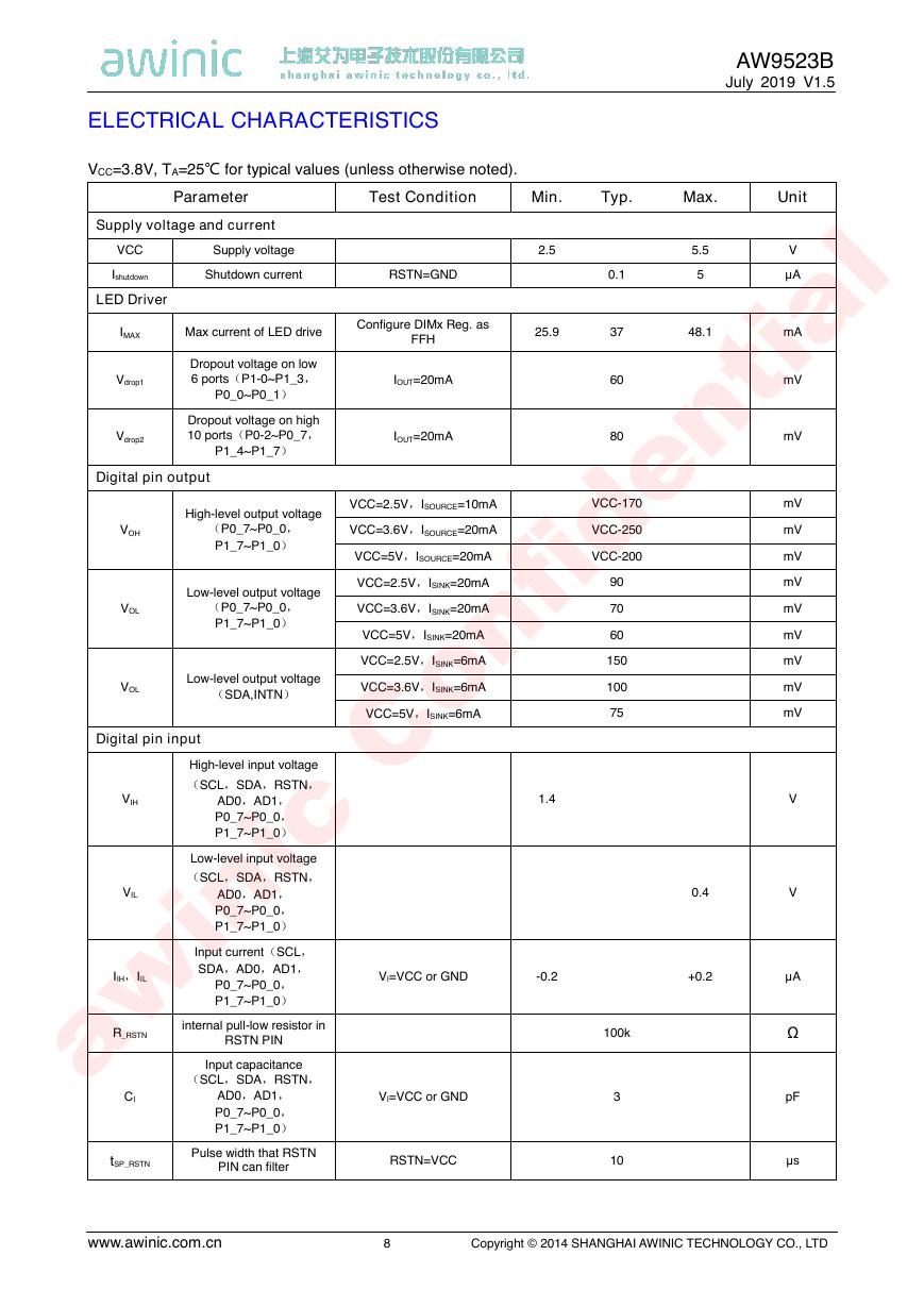
ELECTRICAL CHARACTERISTICS
VCC=3.8V, TA=25℃ for typical values (unless otherwise noted).
Parameter
Test Condition
Min.
Typ.
Max.
Unit
Supply voltage and current
VCC
Ishutdown
LED Driver
Supply voltage
Shutdown current
RSTN=GND
2.5
0.1
IMAX
Max current of LED drive
Configure DIMx Reg. as
FFH
25.9
37
Vdrop1
Vdrop2
Dropout voltage on low
6 ports(P1-0~P1_3,
P0_0~P0_1)
Dropout voltage on high
10 ports(P0-2~P0_7,
P1_4~P1_7)
Digital pin output
VOH
VOL
High-level output voltage
(P0_7~P0_0,
P1_7~P1_0)
Low-level output voltage
(P0_7~P0_0,
P1_7~P1_0)
IOUT=20mA
IOUT=20mA
60
80
VCC-170
VCC-250
VCC-200
VCC=2.5V,ISOURCE=10mA
VCC=3.6V,ISOURCE=20mA
VCC=5V,ISOURCE=20mA
VCC=2.5V,ISINK=20mA
VCC=3.6V,ISINK=20mA
VCC=5V,ISINK=20mA
VCC=2.5V,ISINK=6mA
VCC=3.6V,ISINK=6mA
VCC=5V,ISINK=6mA
48.1
5.5
5
V
μA
mA
mV
mV
mV
mV
mV
mV
mV
mV
mV
mV
mV
V
0.4
V
+0.2
μA
90
70
60
150
100
75
100k
3
10
Ω
pF
μs
Digital pin input
VOL
VIH
VIL
(SDA,INTN)
High-level input voltage
Low-level output voltage
(SCL,SDA,RSTN,
AD0,AD1,
P0_7~P0_0,
P1_7~P1_0)
AD0,AD1,
P0_7~P0_0,
P1_7~P1_0)
Input current(SCL,
SDA,AD0,AD1,
P0_7~P0_0,
P1_7~P1_0)
(SCL,SDA,RSTN,
internal pull-low resistor in
Low-level input voltage
IIH,IIL
R_RSTN
CI
RSTN PIN
Input capacitance
(SCL,SDA,RSTN,
AD0,AD1,
P0_7~P0_0,
P1_7~P1_0)
VI=VCC or GND
VI=VCC or GND
tSP_RSTN
Pulse width that RSTN
PIN can filter
RSTN=VCC
1.4
-0.2
www.awinic.com.cn 8 Copyright © 2014 SHANGHAI AWINIC TECHNOLOGY CO., LTD
�


 V2版本原理图(Capacitive-Fingerprint-Reader-Schematic_V2).pdf
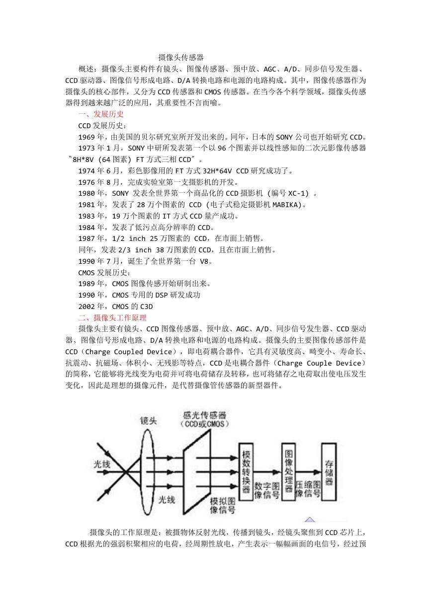 摄像头工作原理.doc
 VL53L0X简要说明(En.FLVL53L00216).pdf
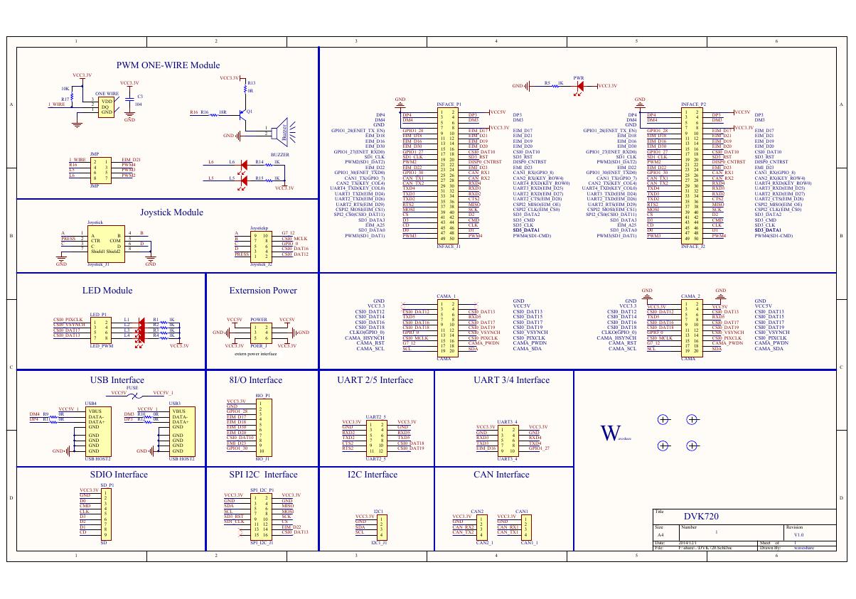 原理图(DVK720-Schematic).pdf
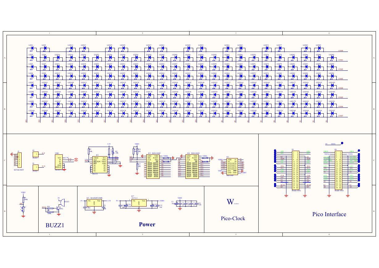 原理图(Pico-Clock-Green-Schdoc).pdf
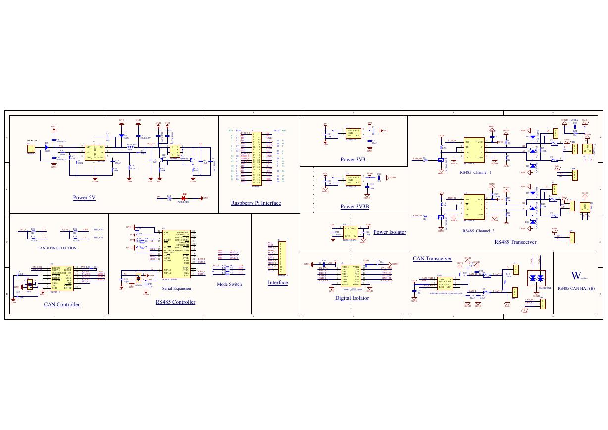 原理图(RS485-CAN-HAT-B-schematic).pdf
 File:SIM7500_SIM7600_SIM7800 Series_SSL_Application Note_V2.00.pdf
 ADS1263(Ads1262).pdf
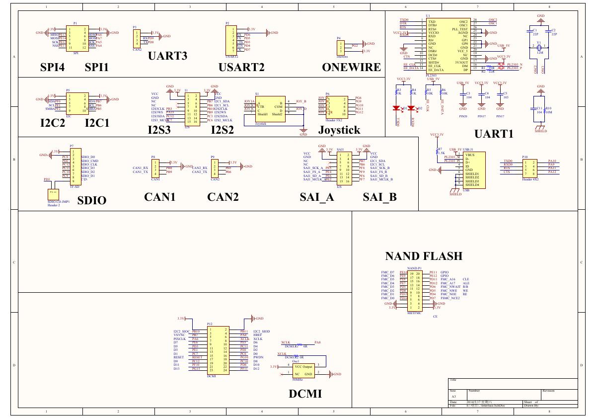 原理图(Open429Z-D-Schematic).pdf
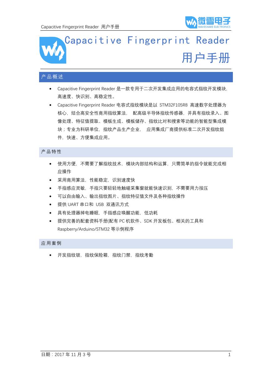 用户手册(Capacitive_Fingerprint_Reader_User_Manual_CN).pdf
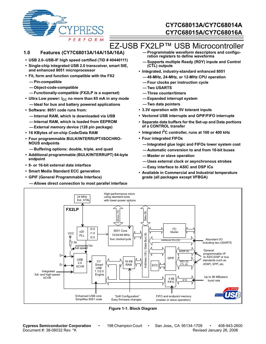 CY7C68013A(英文版)(CY7C68013A).pdf
 TechnicalReference_Dem.pdf