FEATURES
High-Efficiency, 1.5MHz, Synchronous Switching Buck
Charger
90% Charge Efficiency at 2A from 5V Input
Programmable PFM Mode for Light Load Conditions
ETA6953
I2C Controlled 13.5V/3A, 1-Cell Battery Charger with Power Path Management
DESCRIPTION
The ETA6953 is a highly-integrated 3.0-A switch-mode battery
charge management and system power path management
device for single cell Li-Ion and Li-polymer battery. It features fast
charging with high input voltage support for a wide range of smart
phones, tablets and portable devices. Its low impedance power
path optimizes switch-mode operation efficiency, reduces battery
charging time and extends battery life during discharging phase.
Its input voltage and current regulation deliver maximum charging
power to battery. The solution is highly integrated with input
reverse-blocking FET (RBFET, Q1), high-side switching FET
(HSFET, Q2), low-side switching FET (LSFET, Q3), and battery
FET (BATFET, Q4) between system and battery. It also
integrates the bootstrap diode for the high-side gate drive for
simplified system design. The I2C serial interface with charging
and system settings makes the device a truly flexible solution.
Supports USB On-The-Go (OTG)
Up to 1.2A Output
91% Boost Efficiency at 1A Output
Output Short Circuit Protection
Programmable PFM Mode for Light Load Conditions
Wide Range Single Input to Support both USB Input and
High Voltage Adapters
Support 3.9V to 13.5V Input Voltage Range With
Programmable Current Limit Boost Converter with
The device supports a wide range of input sources: standard USB
host port, USB charging port, and USB compliant high voltage
adapter. To support fast charging using high voltage adapter, the
ETA6953 provides PSEL pin for USB switch control. To set the
default input current limit, device takes the result from detection
circuit in the system, such as USB PHY device. The device is
compliant with USB 2.0 and USB 3.0 power spec with input
current and voltage regulation. The device also meets USB On-
the-Go (OTG) operation power rating specification by supplying
5.15 V on VBUS with constant current limit up to 1.2-A.
The power path management regulates the system slightly above
battery voltage but does not drop below 3.5 V minimum system
voltage (programmable). With this feature, the system maintains
operation even when the battery is completely depleted or
removed. When the input current limit or voltage limit is reached,
the power path management automatically reduces the charge
current to zero. As the system load continues to increase, the
power path discharges the battery until the system power
requirement is met. This Supplement Mode prevents overloading
the input source.
The ETA6953 is available in a QFN4x4-24L package.
30V Absolute Maximum Input Voltage Rating
Programmable Input Current Limit (100mA to 3.2A
With 100mA Resolution) to Support USB 2.0, USB
3.0 Standards and High Voltage Adaptors (IINDPM)
High Battery Discharge Efficiency With 27mΩ Battery
Discharge MOSFET
Narrow VDC (NVDC) Power Path Management
BATFET Control to Support Ship Mode, Wake Up and Full
System Reset
Flexible Autonomous and I2C Mode for Optimal System
Performance
High Integration Includes All MOSFETs, Current Sensing
and Loop Compensation
26uA Low Battery Leakage Current to Support Ship Mode
Safety
Battery Temperature Sensing for Charge and Boost
Mode
Thermal Regulation and Thermal Shutdown
Input UVLO and Overvoltage Protection
APPLICATIONS
Tablet PC, Smart Phone, Internet Devices
Portable Audio Speaker
Handheld Computers, PDA, POS
www.etasolution.com
1
Empower, Transcend, Achieve!
�
1 VAC
24 VBUS
23 PMID
7 nINT
3 nPG
6 SDA
5 SCL
9
nCE
2 PSEL
12 nQON
BST
21
SW
19
SW
20
SYS
15
SYS
16
ETA6953
STAT
4
BAT
13
BAT
14
VLDO
22
TS
11
GND
17
GND
18
PART No.
ETA6953Q4Y
PACKAGE
QFN4x4-24
TOP MARK
ETA6953
YWW2L
VSYS
Pcs/Reel
5000
ETA6953
TYPICAL APPLICATION
VBUS
VIO
HOST
USB
PHY
ORDERING INFORMATION
PIN CONFIGURATION
S
U
B
V
24
I
D
M
P
23
O
D
L
V
22
T
S
B
21
W
S
20
W
S
19
ABSOLUTE MAXIMUM RATINGS
(Note: Exceeding these limits may damage the device. Exposure to absolute maximum rating
conditions for long periods may affect device reliability.)
VAC, VBUS, PMID to GND Voltage .........................–2V to 30V
SW to GND Voltage...............................................–0.3V to 20V
nPG, STAT to GND Voltage ..................................–0.3V to 12V
SYS, BAT to GND Voltage.......................................–0.3V to 6V
BST to SW Voltage .................................................–0.3V to 6V
All Other Pin to GND Voltage................................. –0.3V to 6V
SW, VBUS, BAT, SYS to PGND current...........Internally limited
Operating Temperature Range...........................–40°C to 85°C
Storage Temperature Range............................–55°C to 150°C
Thermal Resistance θJA θJC
QFN4x4–24pin...................35................10...................... °C/W
Lead Temperature (Soldering,10sec) .............................260°C
Empower, Transcend, Achieve!
VAC
PSEL
nPG
STAT
SCL
SDA
1
2
3
4
5
6
ETA6953
18
17
16
15
14
GND
GND
SYS
SYS
BAT
GND
13
BAT
7
T
N
n
I
8
C
N
9
E
C
n
10
C
N
11
S
T
12
N
O
Q
n
QFN4 x 4 - 24
www.etasolution.com
2
�
ETA6953
ELECTRICAL CHARACTERISTICS
(Vbat = 3.6V, unless otherwise specified. Typical values are at TA = 25°C.)
PARAMETER
QUIESCENT CURRENTS
Battery discharge current (BAT, SW, SYS)
in buck mode
Battery discharge current (BAT) in buck
mode
Battery discharge current (BAT, SW, SYS)
Input supply current (VBUS) in buck mode
Battery Discharge Current in boost mode
VBUS, VAC AND BAT PIN POWER-UP
VBUS operating range
VBUS for active I2C, no battery Sense
VBUS pin voltage
I2C active hysteresis
One of the conditions to turn on VLDO
One of the conditions to turn on VLDO
Sleep mode falling threshold
Sleep mode rising threshold
VBUS 6.5V Overvoltage rising threshold
VBUS 11V Overvoltage rising threshold
VBUS 14V Overvoltage rising threshold
VBUS 6.5V Overvoltage hysteresis
VAC 11V Overvoltage hysteresis
VAC 14V Overvoltage hysteresis
BAT for active I2C, no adapter
Battery Depletion Threshold
Battery Depletion Threshold
Battery Depletion rising hysteresis
Bad adapter detection falling threshold
Bad adapter detection hysteresis
Bad adapter detection current source
CONDITIONS
MIN
TYP
MAX
UNITS
VBAT = 4.5V, VVBUS < VBUS-UVLOZ,
leakage between BAT and VBUS, TJ< 85°C
VBAT = 4.5V, HIZ Mode and BATFET_DIS = 1 or
No VBUS, I2C disabled, BATFET Disabled.
TJ < 85°C
VBAT = 4.5V, HIZ Mode and OVPFET_DIS = 1
or No VBUS, I2C Disabled, BATFET Enabled.
TJ < 85°C
VVBUS > VBUS_UVLO, VBUS > VBAT, converter
switching, VBAT = 3.8V, ISYS = 0A
VBAT = 4.2V, boost mode, IVBUS = 0A, converter
switching
VVBUS rising
VVBUS rising
VVBUS falling from above VVBUS_UVLO
VVBUS rising
VVBUS falling
(VVBUS–VBAT ), VBUSMIN_FALL ≤ VBAT ≤ VREG, VVBUS
falling
(VVAC–VVBAT ), VBUSMIN_FALL ≤ VBAT
≤ VREG, VAC rising
VVBUS rising, OVP<1:0> = '01’
VVBUS rising, OVP<1:0> = '10'
VVBUS rising, OVP<1:0> = '11'
VVBUS falling, OVP<1:0> = '01’
VVBUS falling, OVP<1:0> = '10'
VVBUS falling, OVP<1:0> = '11'
VBAT rising
VBAT falling
VBAT rising
VBAT rising
VBUS falling
Sink current from VBUS to GND
3.9
15
110
6
10
13
2.5
2.2
2.35
3.7
26
5
50
µA
µA
100
180
µA
5
2
3.3
300
3.65
500
60
220
6.5
11
14
220
400
500
2.7
2.4
2.58
180
3.9
80
30
13.5
3.6
3.9
110
330
7
12
15
2.6
2.8
4.1
mA
mA
V
V
mV
V
mV
mV
mV
V
V
V
mV
mV
mV
V
V
V
mV
V
mV
mA
www.etasolution.com
3
Empower, Transcend, Achieve!
�
ETA6953
PARAMETER
POWER-PATH
System regulation voltage
System Regulation Voltage
Maximum DC system voltage output
Top reverse blocking MOSFET on-
resistance between VBUS and PMID - Q1
Top switching MOSFET on-
resistance between PMID and SW - Q2
Bottom switching MOSFET on-resistance
between SW and GND - Q3
SYS-BAT MOSFET on-resistance – Q4
BATFET forward voltage in supplement
mode
BATTERY CHARGER
Change voltage program range
Charge voltage step
Charge voltage setting
Charge voltage setting accuracy
Charge current regulation range
Charge current regulation step
Charge current regulation setting
Charge current regulation accuracy
Battery LOWV falling threshold
Battery LOWV rising threshold
Precharge current regulation
Termination current regulation
Battery short voltage
Battery short voltage
Battery short current
Recharge Threshold below VBAT_REG
Recharge Threshold below VBAT_REG
INPUT VOLTAGE AND CURRENT REGULATION
Input voltage regulation limit
VBAT < SYS_MIN[2:0] = 101,
BATFET Disabled (REG07[5] = 1)
ISYS = 0A, VBAT > VSYS_MIN, VBAT = 4.400V,
BATFET disabled (REG07[5] = 1)
ISYS = 0A, Q4 off, VBAT≤ 4.400V,
VBAT > VSYSMIN = 3.5V
-40°C≤ TA ≤ 125°C
VVLDO = 5 V , -40°C≤ TA ≤ 125°C
VVLDO = 5 V , -40°C≤ TA ≤ 125°C
QFN package, Measured from BAT
to SYS, VBAT = 4.2V, TJ = –40 - 125°C
VREG (REG04[7:3]) = 4.208 V
(01011), V, –40 ≤ TJ ≤ 85°C
VBAT = 4.208 V or VBAT = 4.352 V,
–40 ≤ TJ ≤ 85°C
ICHG = 1980mA, VVBAT = 3.1V or VVBAT = 3.8V
ICHG = 1980mA, VVBAT = 3.1V or VVBAT = 3.8V
ICHG = 1980mA
Pre-charge to fast charge
IPRECHG[3:0] = '0010' = 180mA
ICHG >780 mA, ITERM[3:0] = '0010'
VVBAT = 4.208V
VVBAT falling
VVBAT rising
VVBAT =1V
VBAT falling, REG04[0] = 0
VBAT falling, REG04[0] = 1
VINDPM[3:0] = 0110 = 4.5 V
CONDITIONS
MIN
TYP
MAX
UNITS
20
35
21
13
3.856
3.68
VBAT+7
0mV
4.47
40
70
43
27
30
32
60
105
65
40
4.624
4.187
4.208
4.229
-0.5
0
-10
2.6
2.9
144
144
1.8
2.05
70
190
4.32
60
1980
2.8
3.1
180
180
2
2.25
145
120
240
4.5
+0.5
3000
+10
3
3.3
216
216
2.2
2.45
170
290
4.68
V
V
mΩ
mΩ
mΩ
mΩ
mV
V
mV
V
%
mA
mA
mA
%
V
V
mA
mA
V
V
mA
mV
mV
V
www.etasolution.com
4
Empower, Transcend, Achieve!
�
ETA6953
PARAMETER
Input voltage regulation accuracy
Input voltage regulation limit tracking
VBAT
USB input current regulation limit
CONDITIONS
VINDPM[3:0] = 3.9V, VDPM_VBAT_TRACK =
300mV, VBAT = 4.0V
VVBUS = 5V, current pulled from SW,
IINDPM [4:0] = 10111 = 2.4 A,
–40 ≤ TJ ≤ 85°C
MIN
-4
4.13
TYP
4.3
MAX
4
4.47
2.16
2.4
2.64
UNITS
%
V
A
mA
%
%
°C
°C
°C
°C
%
%
%
%
%
%
%
%
%
%
%
78
77
29.2
32.4
200
108
103
110
90
160
30
73.3
71.5
68
66.8
44.7
45.7
34.2
35.3
80.0
79.0
31.2
34.4
82
81
33.2
36.4
Temperature Increasing, TREG = 1
Temperature Increasing, TREG = 0
Charger suspends charge. As Percentage to
VLDO
As Percentage to VLDO
VBAT rising, as percentage of VBAT_REG
VBAT falling, as percentage of VBAT_REG
Input current limit during system start-up
sequence
BAT PIN OVERVOLTAGE PROTECTION
Battery overvoltage threshold
Battery overvoltage threshold Hysteresis
THERMAL REGULATION AND THERMAL SHUTDOWN
Junction Temperature Regulation
Threshold
Junction Temperature Regulation
Threshold
Thermal Shutdown Rising Temperature
Thermal Shutdown Hysteresis
JEITA Thermistor Comparator (BUCK MODE)
T1 (0°C) threshold, Charge suspended T1
below this temperature.
Falling
T2 (10°C) threshold, Charge back to
ICHG/2 and 4.2 V below this temperature
Falling
T3 (45°C) threshold, charge back to ICHG
and 4.05V above this temperature.
Falling
T5 (60°C) threshold, charge suspended
above this temperature.
Falling
As Percentage to VLDO
COLD OR HOT THERMISTER COMPARATOR (BOOST MODE)
As Percentage to VLDO (Approx. -20°C w/
Cold Temperature Threshold, TS pin
103AT), TJ = –20°C - 125°C
Voltage Rising Threshold
TJ = –20°C - 125°C
Falling
As Percentage to VLDO (Approx. 60°C w/
Hot Temperature Threshold, TS pin
103AT), TJ = –20°C - 125°C
Voltage falling Threshold
Rising
TJ = –20°C - 125°C
CHARGE OVERCURRENT COMPARATOR (CYCLE-BY-CYCLE)
As Percentage to VLDO
Charger suspends charge. As Percentage to
VLDO
As Percentage to VLDO
As Percentage to VLDO
As Percentage to VLDO
www.etasolution.com
5
Empower, Transcend, Achieve!
�
ETA6953
PARAMETER
CONDITIONS
HSFET cycle-by-cycle over-current
threshold
System over load threshold
CHARGE UNDER-CURRENT COMPARATOR (CYCLE-BY-CYCLE)
LSFET under-current falling threshold
PWM
PWM switching frequency
Maximum PWM duty cycle
BOOST MODE OPERATION
Boost mode regulation voltage
Boost mode regulation voltage accuracy
Oscillator frequency
From sync mode to non-sync mode
VVBUS = 9V, ILDO = 40mA
VVBUS = 9V, VLDO = 4V
VLDO REGULATION
LDO output voltage
LDO output current limit
LOGIC I/O PIN CHARACTERISTICS (nCE, PSEL, SCL, SDA)
Input low threshold
Input high threshold
High-level leakage current
LOGIC I/O PIN CHARACTERISTICS (nPG, STAT, nINT)
Low-level output voltage
VBUS/BAT POWER UP
Bad adapter detection duration
BATTERY CHARGER
Deglitch time for charge Termination
Deglitch time for recharge
System over-current deglitch time to turn
off Q4
Pull up rail 1.8 V
Battery voltage exiting boost mode
OTG mode output current
OTG overvoltage threshold
HSFET under current falling threshold
Hiccup Retrying timer
Hiccup Off timer
Maximum retry allowed
VVBAT = 3.8 V, I(PMID) = 0 A, BOOSTV[1:0] = '10'
VVBAT = 3.8 V, I(PMID) = 0 A, BOOSTV[1:0] = '10'
VVBAT falling, MIN_VBAT_SEL = 0
VVBAT rising, MIN_VBAT_SEL =0
VVBAT falling, MIN_VBAT_SEL = 1
VVBAT rising, MIN_VBAT_SEL = 1
BOOST_LIM = 1
BOOST_LIM = 0
Rising threshold
After the last retry, part clear OTG_CONFIG
bit to disable Boost
MIN
4.8
4.7
5
-3
2.6
2.8
2.3
2.6
1.2
0.5
5.6
1.3
TYP
MAX
UNITS
5.8
5.2
250
1500
97
5.15
2.8
3
2.5
2.8
1.4
0.7
6
100
7
28
7
5
80
30.0
7
32
1
7.5
5.7
5.3
3
3.0
3.2
2.7
3.0
6.4
0.4
1
0.4
A
A
mA
kHz
%
V
%
V
V
V
V
A
A
V
mA
ms
ms
Time
V
mA
V
V
µA
V
ms
s
ms
ms
www.etasolution.com
6
Empower, Transcend, Achieve!
�
ETA6953
PARAMETER
Battery over-voltage deglitch time to
disable charge
Typical Charge Safety Timer Range
Typical Top-Off Timer Range
nQON TIMING
nQON low time to turn on BATFET and
exit ship mode
nQON low time to reset BATFET
BATFET off time during full system reset
Enter ship mode delay
DIGITAL CLOCK AND WATCHDOG TIMER
REG05[4]=01
CONDITIONS
MIN
TYP
MAX
UNITS
CHG_TIMER = 1
TOP_OFF_TIMER[1:0] = 10 (30 min)
–10oC ≤ TJ ≤ 60oC
–10oC ≤ TJ ≤ 60oC
–10oC ≤ TJ ≤ 60oC
–10 oC ≤ TJ ≤ 60oC
10
10
30
1.15
10
320
12
40
µs
Hr
min
s
s
ms
s
s
PIN DESCRIPTION
PIN #
PIN NAME
1
VAC
VBUS
PSEL
nPG
STAT
SCL
SDA
nINT
NC
nCE
NC
TS
24
2
3
4
5
6
7
8
9
10
11
DESCRIPTION
Charger input voltage sense. This pin must be connected to VBUS pin.
Charger input voltage. Bypass it with a 10-μF ceramic capacitor from VBUS to PGND. The capacitor
should be close to the VBUS pin.
Power source selection input. Set 500 mA input current limit by pulling this pin high and set 2.4A
input current limit by pulling this pin low. Once the device gets into host mode, the host can program
different input current limits to IINDPM register.
Open drain active low power good indicator. Connect to the pull up rail through 10-kΩ resistor. LOW
indicates a good input source if the input voltage is between VBUSUVLO and VBUS_OV, above SLEEP
mode threshold, and current limit is above 30 mA.
Open-drain charge status output. Connect the STAT pin to a logic rail via 10-kΩ resistor. The STAT
pin indicates charger status. Connect a current limit resistor and a LED from a rail to this pin.
Charge in progress: LOW
Charge complete or charger in SLEEP mode: HIGH
Charge suspend (fault response)or No bat: 1-Hz, 50% duty cycle Pulses
I2C interface clock. Connect a 10-kΩ pull up resistor to the logic rail.
I2C interface data. Connect a 10-kΩ pull up resistor to the logic rail.
Open-drain interrupt Output. Connect the INT to a logic rail through 10-kΩ resistor. The INT pin
sends an active low, 256-µs pulse to host to report charger device status and fault.
No Connect. Keep the pin float
Charge disable control pin. nCE=0, charge is enabled. nCE=1, charge is disabled.
No Connect. Keep the pin float
Temperature qualification voltage input to support JEITA profile. Connect a negative temperature
coefficient thermistor. Program temperature window with a resistor divider from VLDO to TS to GND.
www.etasolution.com
7
Empower, Transcend, Achieve!
�
ETA6953
PIN NAME
PIN #
nQON
12
BAT
SYS
GND
SW
BST
VLDO
PMID
EP
13, 14
15, 16
17, 18
19, 20
21
22
23
EP
DESCRIPTION
Charge suspends when either TS pin is out of range. When TS pin is not used, connect a 10-kΩ
resistor from VLDO to TS and connect a 10-kΩ resistor from TS to GND. It is recommended to use
a 103AT-2 thermistor.
BATFET enable/reset control input. When BATFET is in ship mode, a logic low of tSHIPMODE (typical
1.15s) duration turns on BATFET to exit shipping mode. When VBUS is not plugged-in, a logic low
of tQON_RST (minimum 8s) duration resets SYS (system power) by turning BATFET off for tBATFET_RST
(minimum 250 ms) and then re-enable BATFET to provide full system power reset. The pin contains
an internal pull-up to maintain default high logic.
Positive battery terminal. The internal BATFET and current sensing is connected between SYS and
BAT. Connect a 10 μF close to the BAT pin.
Converter output connection point. The internal current sensing network is connected between SYS
and BAT. Connect a 20 μF close to the SYS pin.
Power Ground
Switching node output. Connected to output inductor. Connect the 10nF bootstrap capacitor from
SW to BTST
Bootstrap capacitor connection for the high-side FET gate driver. Connect a 10nF ceramic capacitor
from BST pin to SW pin.
LDO Output Voltage. Bypass the pin with 4.7μF (10V rating) capacitor from VLDO to GND. The
capacitor should be closed to the pin
Connection point between reverse blocking FET and high-side switching FET. Bypass it with a
minimum of 10μF capacitor from PMID to PGND. This capacitor should be close to the PMID pin.
Thermal pad and ground reference. This pad is ground reference for the device and it is also the
thermal pad used to conduct heat from the device. This pad should be tied externally to a ground
plane through PCB vias under the pad.
TYPICAL PERFORMANCE CHARACTERISTICS
(Typical values are at TA = 25oC unless otherwise specified.)
)
V
(
t
u
o
V
5.5
5.4
5.3
5.2
5.1
5
4.9
4.8
4.7
4.6
4.5
OTG Vout Vs. Iout
Vout=5.1V
Vbat=3.3V
Vbat=3.6V
Vbat=3.8V
Vbat=4.2V
Vbat=4.35V
0
0.2
0.4
0.6
Iout (A)
0.8
1
1.2
www.etasolution.com
8
)
%
(
y
c
n
e
i
c
i
f
f
E
100%
95%
90%
85%
80%
75%
70%
65%
60%
55%
50%
OTG Eff. Vs. Iout
Vout=5.1V
Vbat=3.3V
Vbat=3.6V
Vbat=3.8V
Vbat=4.2V
Vbat=4.35V
1
0.01
0.1
Iout (A)
Empower, Transcend, Achieve!
�
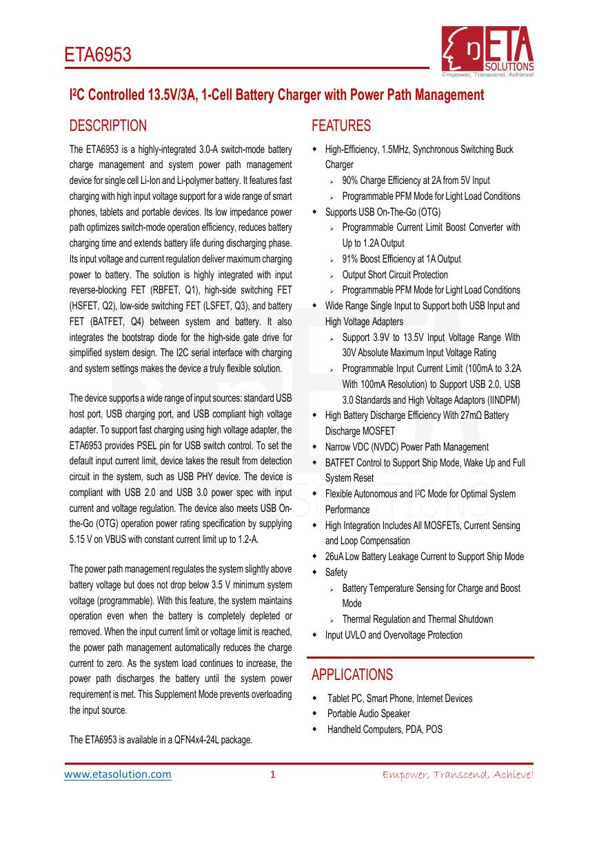


 V2版本原理图(Capacitive-Fingerprint-Reader-Schematic_V2).pdf
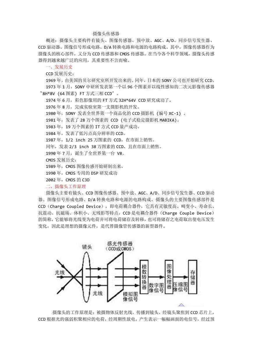 摄像头工作原理.doc
 VL53L0X简要说明(En.FLVL53L00216).pdf
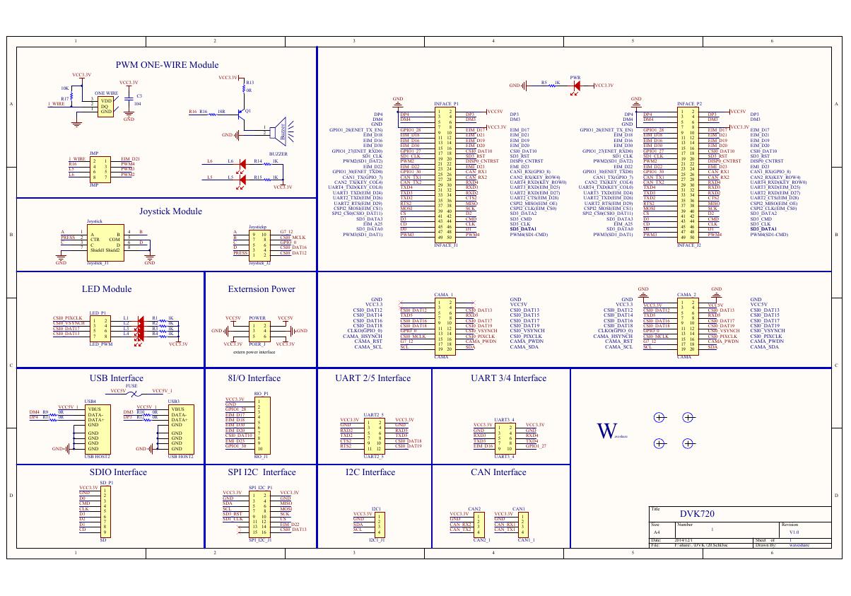 原理图(DVK720-Schematic).pdf
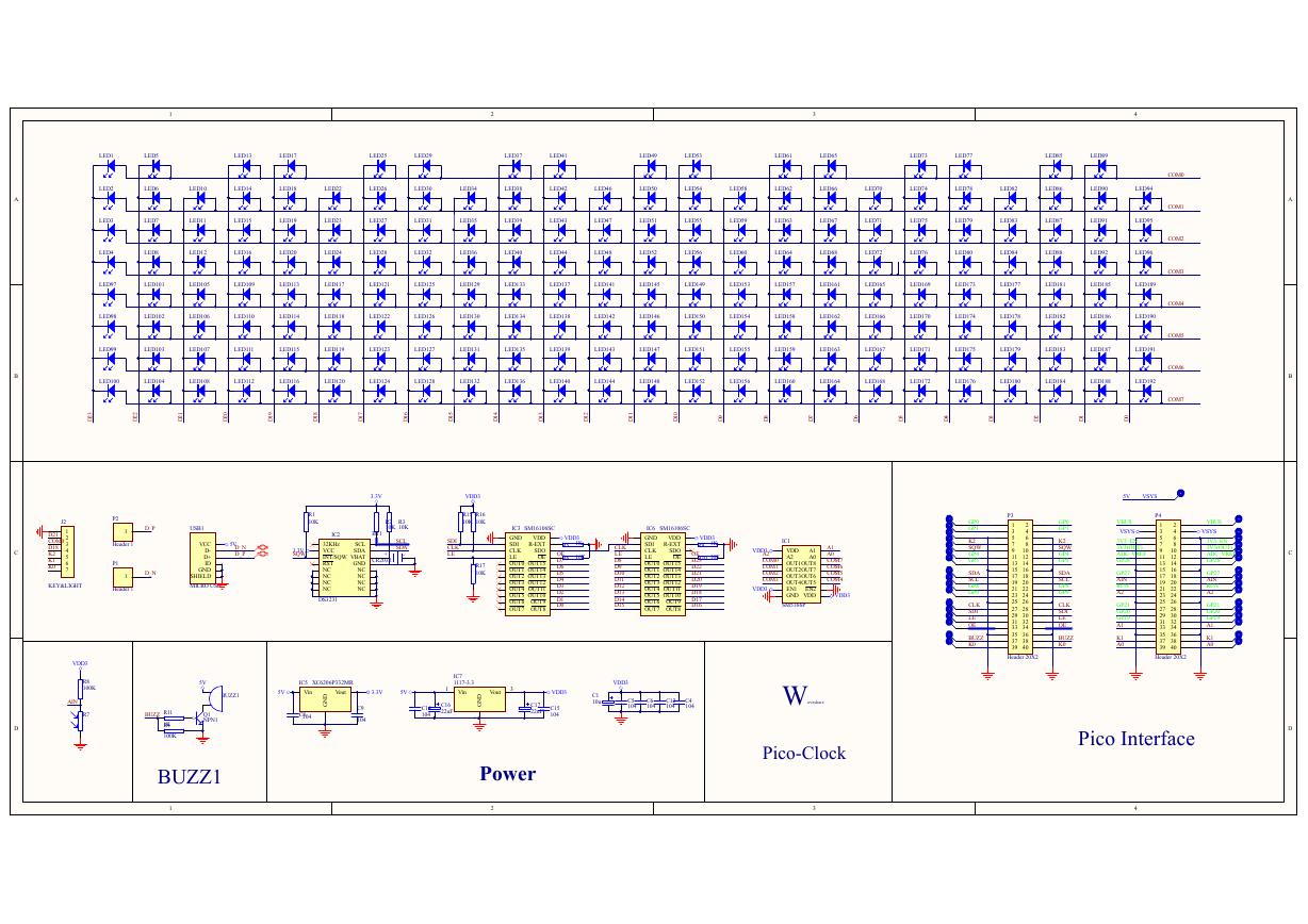 原理图(Pico-Clock-Green-Schdoc).pdf
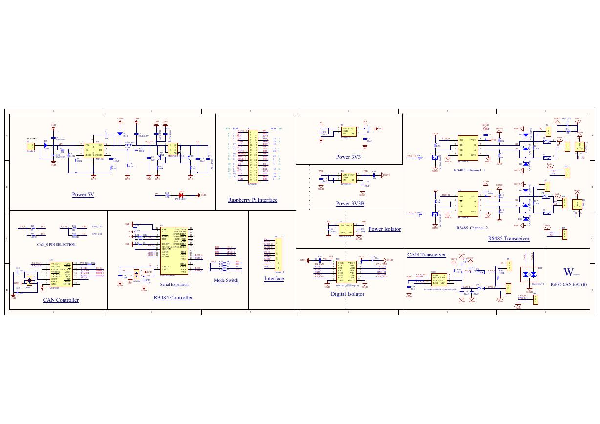 原理图(RS485-CAN-HAT-B-schematic).pdf
 File:SIM7500_SIM7600_SIM7800 Series_SSL_Application Note_V2.00.pdf
 ADS1263(Ads1262).pdf
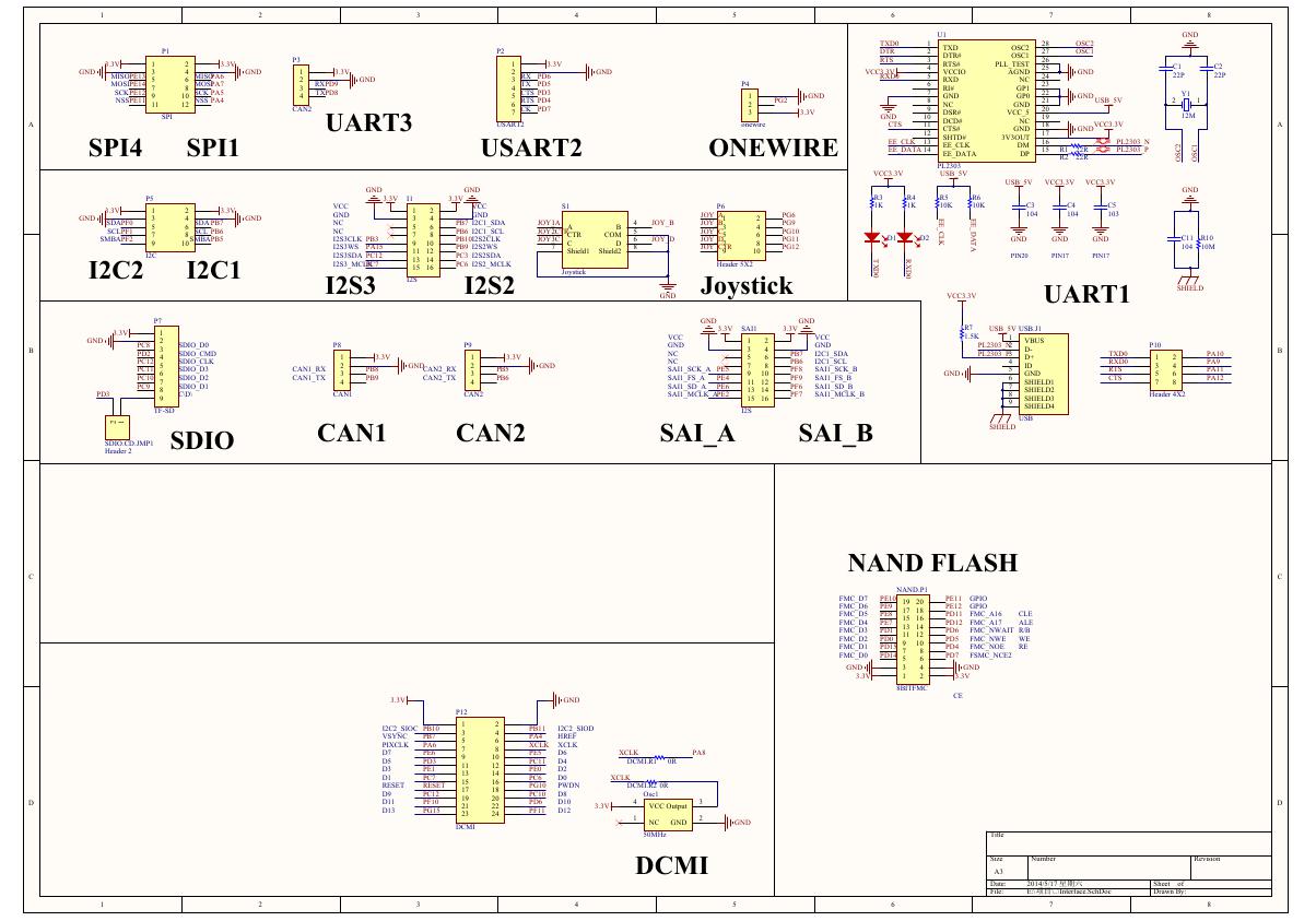 原理图(Open429Z-D-Schematic).pdf
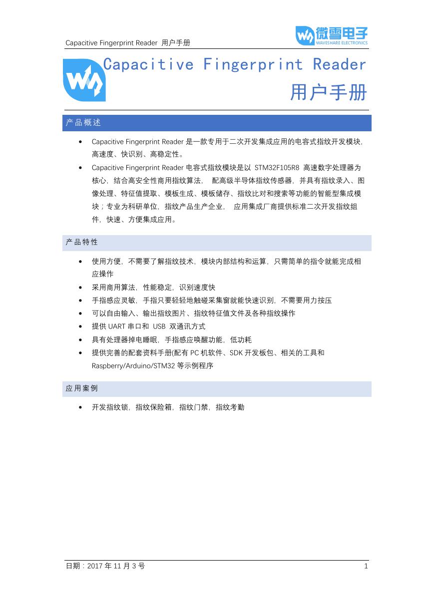 用户手册(Capacitive_Fingerprint_Reader_User_Manual_CN).pdf
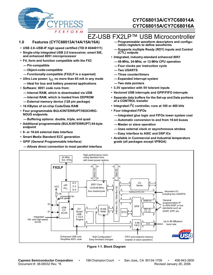 CY7C68013A(英文版)(CY7C68013A).pdf
 TechnicalReference_Dem.pdf