/
Preface
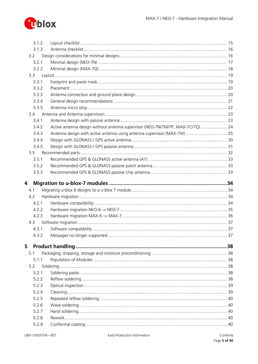
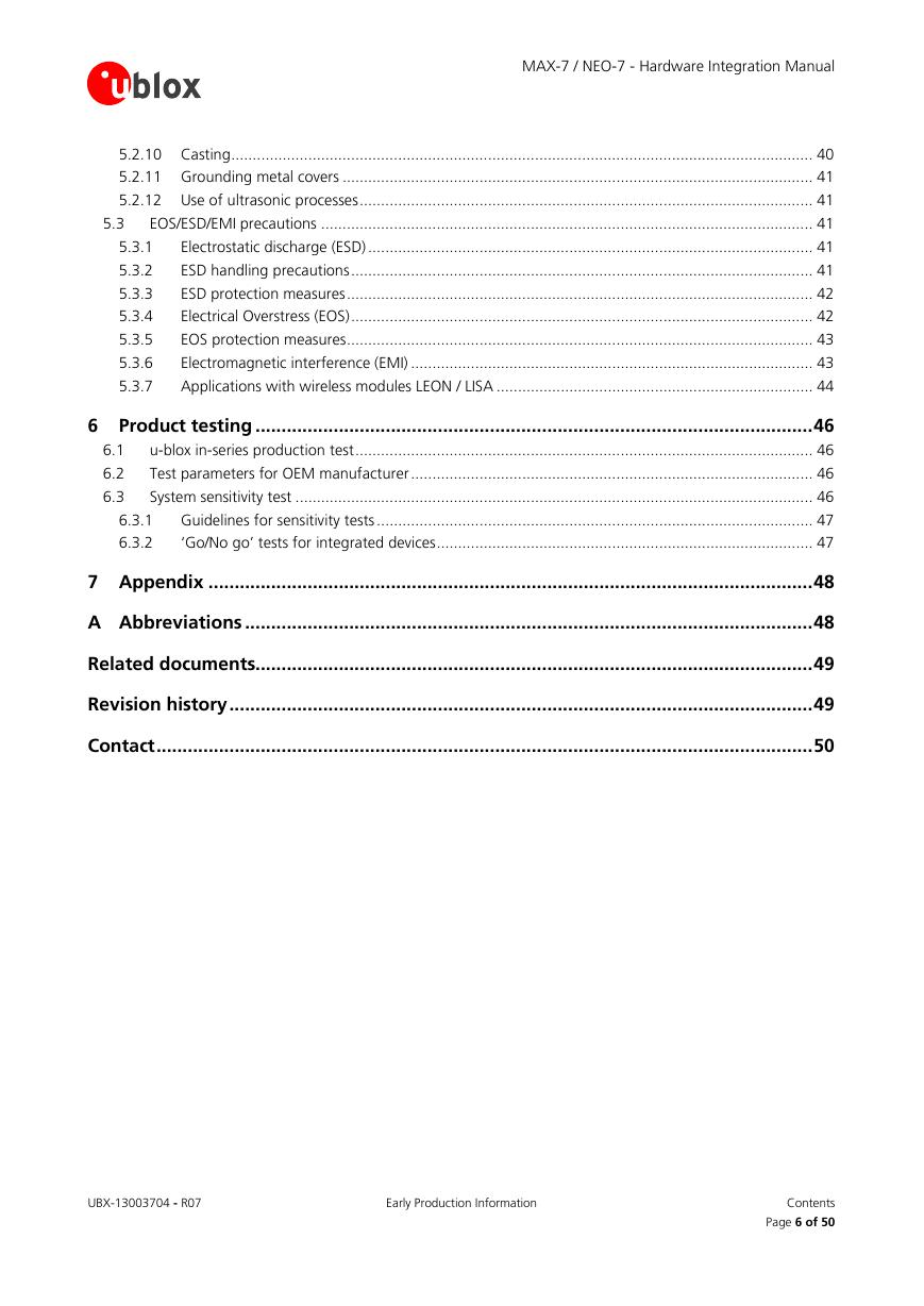
Contents
1 Quick reference
2 Hardware description
2.1 Overview
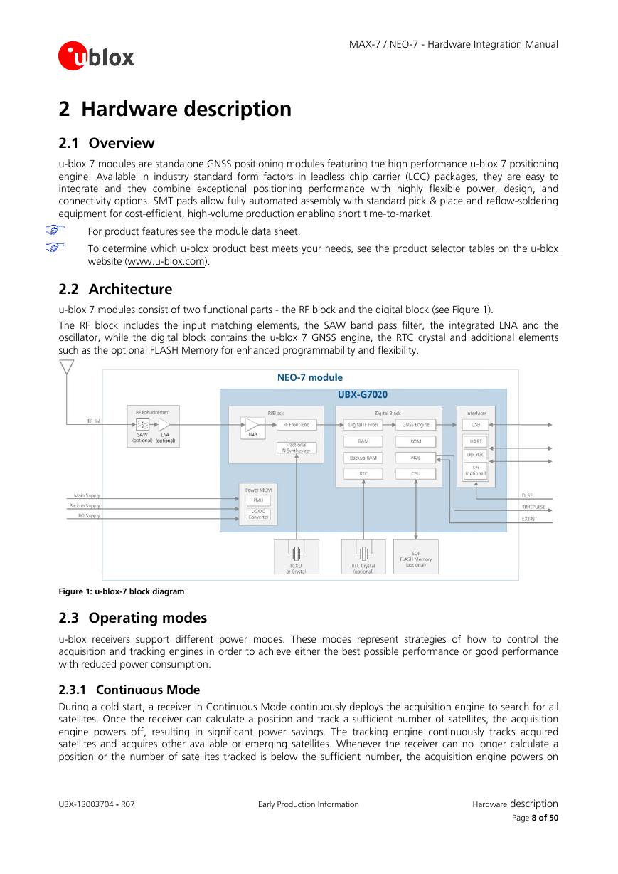
2.2 Architecture
2.3 Operating modes
2.3.1 Continuous Mode
2.3.2 Power Save Mode
2.4 Configuration
2.4.1 Electrical Programmable Fuse (eFuse)
2.5 Connecting power
2.5.1 VCC: Main supply voltage
2.5.2 VCC_IO: IO supply voltage (MAX-7)
2.5.3 V_BCKP: Backup supply voltage
2.5.3.1 RTC derived from the system clock; “Single Crystal” feature (MAX-7C)
2.5.4 VDD_USB: USB interface power supply (NEO-7)
2.5.5 VCC_RF: Output voltage RF section
2.5.6 V_ANT: Antenna supply (MAX-7W)
2.6 Interfaces
2.6.1 UART
2.6.2 USB
2.6.2.1 USB external components
2.6.3 Display Data Channel (DDC)
2.6.4 SPI (NEO-7)
2.7 I/O pins
2.7.1 RESET_N: Reset input
2.7.2 EXTINT: External interrupt
2.7.3 D_SEL: Interface select (NEO-7)
2.7.4 TX Ready signal
2.7.5 ANT_ON: Antenna ON (LNA enable) (NEO-7N, MAX-7Q, MAX-7C)
2.7.6 Antenna Short circuit detection (MAX-7W)
2.7.7 Antenna open circuit detection
2.7.7.1 Antenna open circuit detection (MAX-7)
2.7.8 Time pulse
3 Design
3.1 Design checklist
3.1.1 Schematic checklist
3.1.2 Layout checklist
3.1.3 Antenna checklist
3.2 Design considerations for minimal designs
3.2.1 Minimal design (NEO-7N)
3.2.2 Minimal design (MAX-7Q)
3.3 Layout
3.3.1 Footprint and paste mask
3.3.2 Placement
3.3.3 Antenna connection and ground plane design
3.3.4 General design recommendations:
3.3.5 Antenna micro strip
3.4 Antenna and Antenna supervision
3.4.1 Antenna design with passive antenna
3.4.1.1 Minimal setup with a good patch antenna
3.4.1.2 Setup for best performance with passive antenna
3.4.2 Active antenna design without antenna supervisor (NEO-7N/7M/7P, MAX-7C/7Q)
3.4.2.1 Active antenna design, VCC_RF used to supply active antenna
3.4.2.2 Active antenna design powered from external supply
3.4.3 Antenna design with active antenna using antenna supervisor (MAX-7W)
3.4.3.1 Status reporting
3.4.3.2 Module design with active antenna, short circuit protection / detection (MAX-7W)
3.4.3.3 Antenna supervision open circuit detection (OCD) (MAX-7W)
3.4.3.4 External active antenna supervisor using customer uP (NEO-7N, MAX-7Q, MAX-7C)
3.4.3.5 External active antenna control (NEO-7N, MAX-7Q, MAX-7C)
3.4.4 Design with GLONASS / GPS active antenna
3.4.5 Design with GLONASS / GPS passive antenna
3.5 Recommended parts
3.5.1 Recommended GPS & GLONASS active antenna (A1)
3.5.2 Recommended GPS & GLONASS passive patch antenna
3.5.3 Recommended GPS & GLONASS passive chip antenna
4 Migration to u-blox-7 modules
4.1 Migrating u-blox 6 designs to a u-blox 7 module
4.2 Hardware migration
4.2.1 Hardware compatibility:
4.2.2 Hardware migration NEO-6 -> NEO-7
4.2.3 Hardware migration MAX-6 -> MAX-7
4.3 Software migration
4.3.1 Software compatibility
4.3.2 Messages no longer supported
5 Product handling
5.1 Packaging, shipping, storage and moisture preconditioning
5.1.1 Population of Modules
5.2 Soldering
5.2.1 Soldering paste
5.2.2 Reflow soldering
5.2.3 Optical inspection
5.2.4 Cleaning
5.2.5 Repeated reflow soldering
5.2.6 Wave soldering
5.2.7 Hand soldering
5.2.8 Rework
5.2.9 Conformal coating
5.2.10 Casting
5.2.11 Grounding metal covers
5.2.12 Use of ultrasonic processes
5.3 EOS/ESD/EMI precautions
5.3.1 /Electrostatic discharge (ESD)
5.3.2 ESD handling precautions
5.3.3 ESD protection measures
5.3.4 Electrical Overstress (EOS)
5.3.5 EOS protection measures
5.3.6 Electromagnetic interference (EMI)
5.3.7 Applications with wireless modules LEON / LISA
5.3.7.1 Isolation between GPS and GSM antenna
5.3.7.2 Increasing jamming immunity
5.3.7.3 In-band jamming
5.3.7.4 Out-band jamming
6 Product testing
6.1 u-blox in-series production test
6.2 Test parameters for OEM manufacturer
6.3 System sensitivity test
6.3.1 Guidelines for sensitivity tests
6.3.2 ‘Go/No go’ tests for integrated devices
7 Appendix
A Abbreviations
Related documents
Revision history
Contact


 V2版本原理图(Capacitive-Fingerprint-Reader-Schematic_V2).pdf
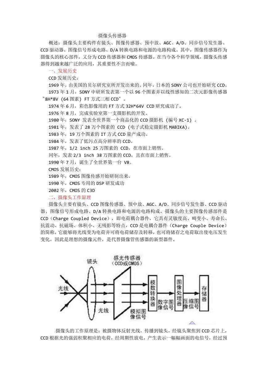 摄像头工作原理.doc
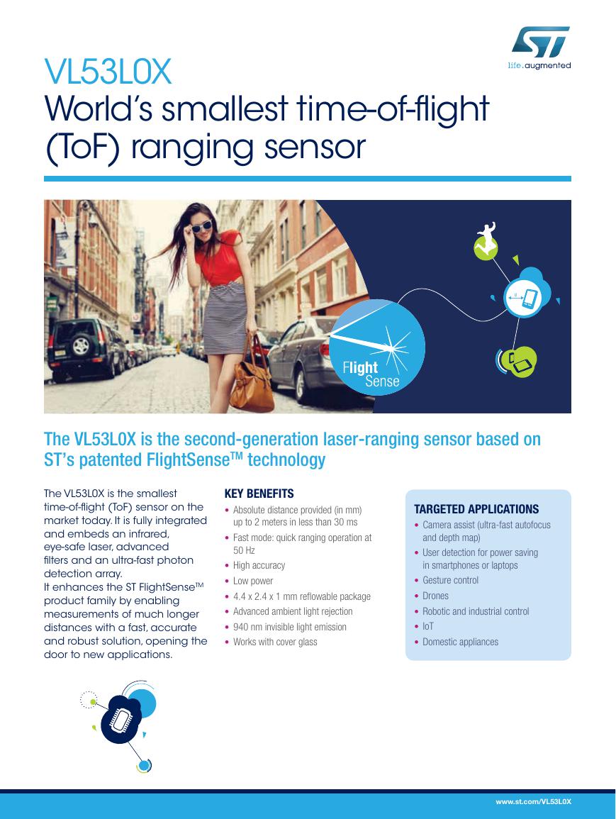 VL53L0X简要说明(En.FLVL53L00216).pdf
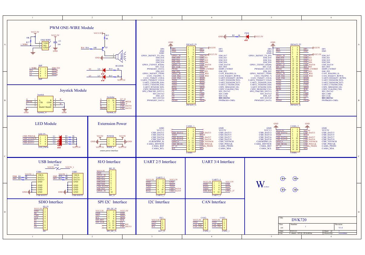 原理图(DVK720-Schematic).pdf
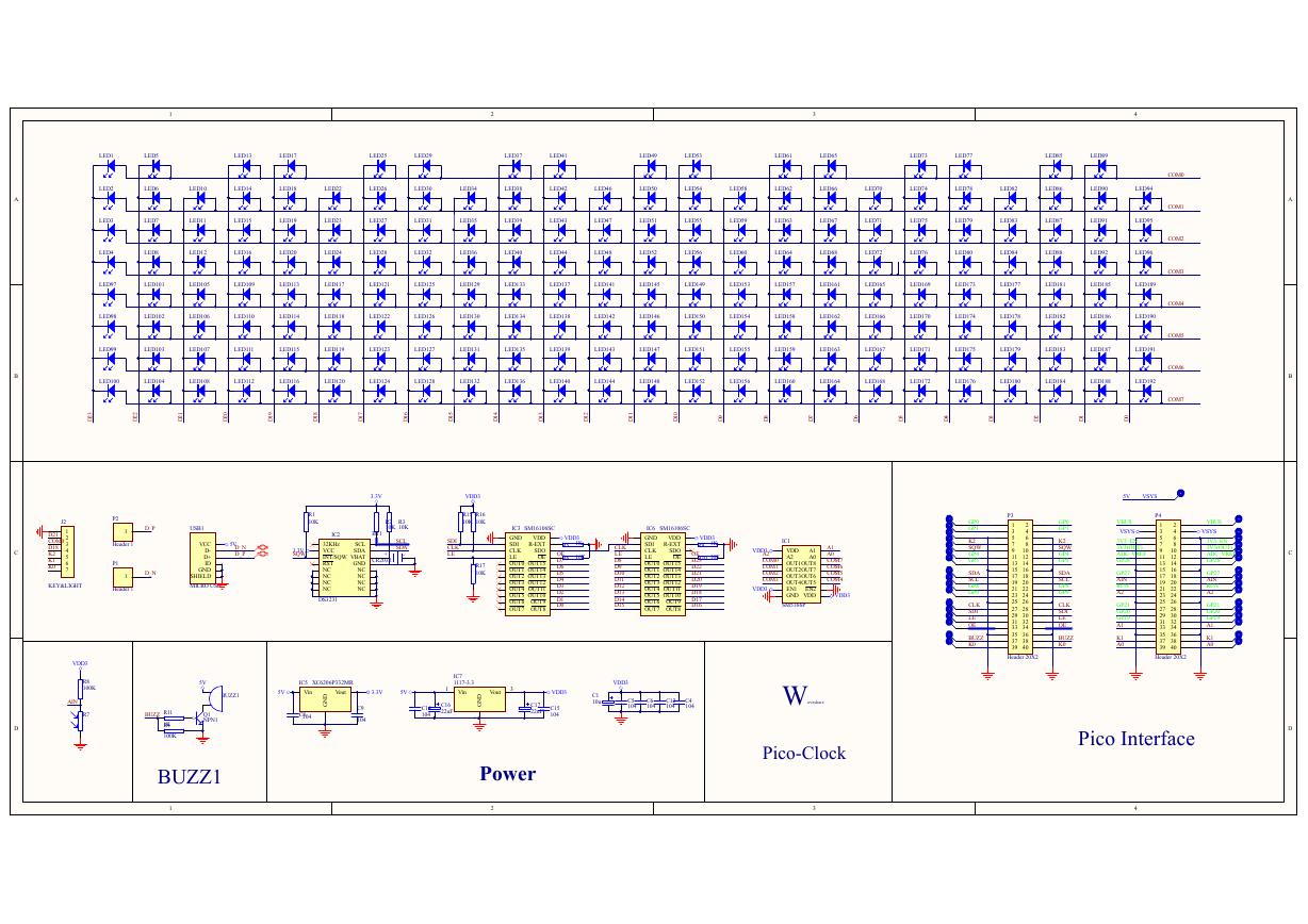 原理图(Pico-Clock-Green-Schdoc).pdf
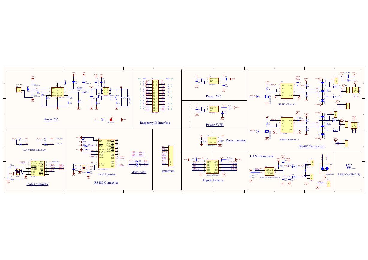 原理图(RS485-CAN-HAT-B-schematic).pdf
 File:SIM7500_SIM7600_SIM7800 Series_SSL_Application Note_V2.00.pdf
 ADS1263(Ads1262).pdf
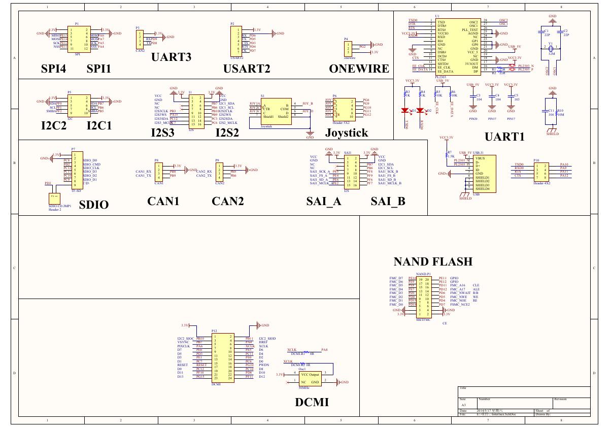 原理图(Open429Z-D-Schematic).pdf
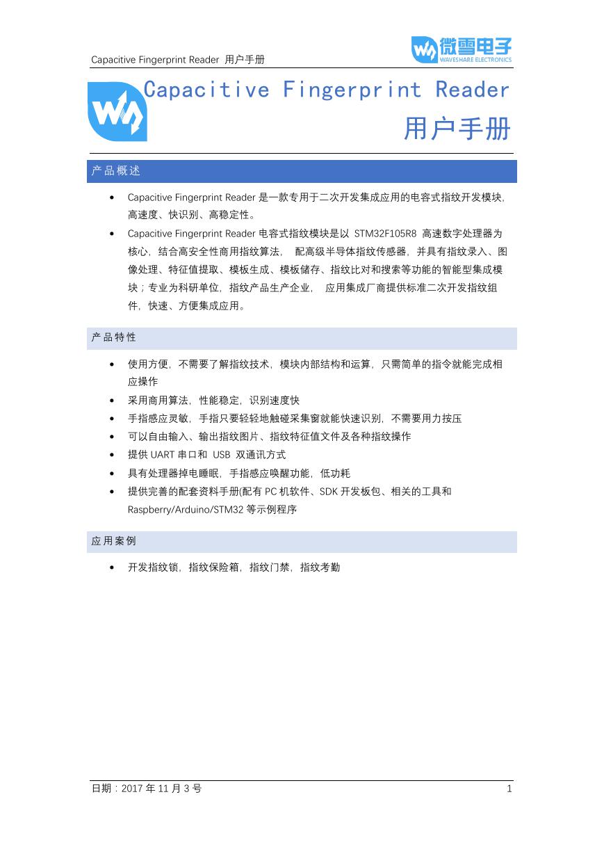 用户手册(Capacitive_Fingerprint_Reader_User_Manual_CN).pdf
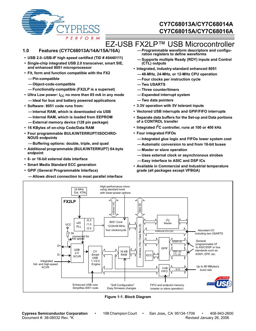 CY7C68013A(英文版)(CY7C68013A).pdf
 TechnicalReference_Dem.pdf