September 2002
B
S
S
1
3
8
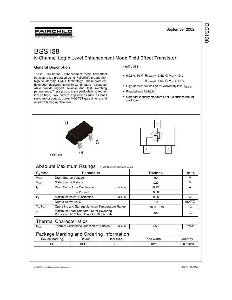
BSS138
N-Channel Logic Level Enhancement Mode Field Effect Transistor
General Description
These N-Channel enhancement mode field effect
transistors are produced using Fairchild’s proprietary,
high cell density, DMOS technology. These products
have been designed to minimize on-state resistance
while provide rugged, reliable, and fast switching
performance.These products are particularly suited for
low voltage, low current applications such as small
servo motor control, power MOSFET gate drivers, and
other switching applications.
Features
• 0.22 A, 50 V. RDS(ON) = 3.5Ω @ VGS = 10 V
RDS(ON) = 6.0Ω @ VGS = 4.5 V
• High density cell design for extremely low RDS(ON)
• Rugged and Reliable
• Compact industry standard SOT-23 surface mount
package
D
D
SOT-23
G
S
– Pulsed
Parameter
Absolute Maximum Ratings TA=25oC unless otherwise noted
Symbol
VDSS
VGSS
ID
PD
Drain-Source Voltage
Gate-Source Voltage
Drain Current – Continuous
Maximum Power Dissipation
Derate Above 25°C
Operating and Storage Junction Temperature Range
Maximum Lead Temperature for Soldering
Purposes, 1/16” from Case for 10 Seconds
TJ, TSTG
TL
Thermal Characteristics
RθJA
Package Marking and Ordering Information
Thermal Resistance, Junction-to-Ambient
(Note 1)
(Note 1)
(Note 1)
Device Marking
SS
Device
BSS138
Reel Size
7’’
G
S
Ratings
Units
50
±20
0.22
0.88
0.36
2.8
−55 to +150
300
350
V
V
A
W
mW/°C
°C
°C
°C/W
Tape width
8mm
Quantity
3000 units
2002 Fairchild Semiconductor Corporation
BSS138 Rev B(W)
�
TA = 25°C unless otherwise noted
Test Conditions
Min Typ Max Units
B
S
S
1
3
8
Parameter
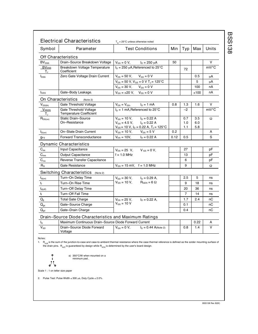
Electrical Characteristics
Symbol
Off Characteristics
BVDSS
∆BVDSS
∆TJ
IDSS
IGSS
On Characteristics
VGS(th)
∆VGS(th)
∆TJ
RDS(on)
Gate Threshold Voltage
Gate Threshold Voltage
Temperature Coefficient
Static Drain–Source
On–Resistance
(Note 2)
ID = 250 µA
Drain–Source Breakdown Voltage VGS = 0 V,
Breakdown Voltage Temperature
Coefficient
Zero Gate Voltage Drain Current
Gate–Body Leakage.
ID = 250 µA,Referenced to 25°C
VDS = 50 V,
VDS = 50 V, VGS = 0 V TJ = 125°C
VDS = 30 V,
VGS = 0 V
VGS = ±20 V, VDS = 0 V
VGS = 0 V
ID = 1 mA
VDS = VGS,
ID = 1 mA,Referenced to 25°C
VGS = 10 V,
VGS = 4.5 V,
VGS = 10 V, ID = 0.22 A, TJ = 125°C
VGS = 10 V,
VDS = 10V,
VDS = 5 V
ID = 0.22 A
ID = 0.22 A
ID = 0.22 A
50
0.8
0.2
0.12
72
1.3
–2
0.7
1.0
1.1
0.5
27
13
6
9
2.5
9
20
7
1.7
0.1
0.4
0.8
0.5
5
100
±100
1.6
3.5
6.0
5.8
5
18
36
14
2.4
0.22
1.4
V
mV/°C
µA
µA
nA
nA
V
mV/°C
Ω
A
S
pF
pF
pF
Ω
ns
ns
ns
ns
nC
nC
nC
A
V
V GS = 0 V,
VGS = 15 mV,
VDS = 25 V,
f = 1.0 MHz
On–State Drain Current
Forward Transconductance
ID(on)
gFS
Dynamic Characteristics
Input Capacitance
Ciss
Output Capacitance
Coss
Crss
Reverse Transfer Capacitance
RG
Gate Resistance
Switching Characteristics (Note 2)
td(on)
tr
td(off)
tf
Qg
Qgs
Qgd
Drain–Source Diode Characteristics and Maximum Ratings
IS
VSD
Turn–On Delay Time
Turn–On Rise Time
Turn–Off Delay Time
Turn–Off Fall Time
Total Gate Charge
Gate–Source Charge
Gate–Drain Charge
Maximum Continuous Drain–Source Diode Forward Current
Drain–Source Diode Forward
Voltage
VDS = 25 V,
VGS = 10 V
ID = 0.29 A,
RGEN = 6 Ω
VDD = 30 V,
VGS = 10 V,
ID = 0.22 A,
f = 1.0 MHz
VGS = 0 V,
IS = 0.44 A(Note 2)
Notes:
1. RθJA is the sum of the junction-to-case and case-to-ambient thermal resistance where the case thermal reference is defined as the solder mounting surface of
the drain pins. RθJC is guaranteed by design while RθCA is determined by the user's board design.
a) 350°C/W when mounted on a
minimum pad..
Scale 1 : 1 on letter size paper
2. Pulse Test: Pulse Width ≤ 300 µs, Duty Cycle ≤ 2.0%
BSS138 Rev B(W)
�
Typical Characteristics
VGS = 10V
6.0V
4.5V
3.5V
3.0V
2.5V
2.0V
)
A
(
T
N
E
R
R
U
C
N
A
R
D
I
,
D
I
1
0.8
0.6
0.4
0.2
0
0
B
S
S
1
3
8
3.4
3
2.6
2.2
1.8
1.4
1
0.6
VGS = 2.5V
3.0V
3.5V
4.0V
4.5V
6.0V
10V
I
D
E
Z
L
A
M
R
O
N
,
)
N
O
S
D
R
(
I
-
E
C
N
A
T
S
S
E
R
N
O
E
C
R
U
O
S
N
A
R
D
-
I
0.5
1
1.5
2
2.5
3
VDS, DRAIN TO SOURCE VOLTAGE (V)
0
0.2
0.4
0.6
0.8
1
ID, DRAIN CURRENT (A)
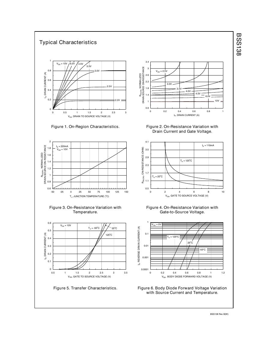
Figure 1. On-Region Characteristics.
Figure 2. On-Resistance Variation with
Drain Current and Gate Voltage.
125
150
0
2
1.8
1.6
1.4
1.2
1
0.8
0.6
ID = 220mA
VGS = 10V
-50
-25
25
0
100
TJ, JUNCTION TEMPERATURE (oC)
50
75
Figure 3. On-Resistance Variation with
Temperature.
0.6
0.5
0.4
0.3
0.2
0.1
0
0.5
VDS = 10V
TA = -55oC
25oC
125oC
1
1.5
2
2.5
3
3.5
VGS, GATE TO SOURCE VOLTAGE (V)
Figure 5. Transfer Characteristics.
I
D
E
Z
L
A
M
R
O
N
,
)
N
O
S
D
R
(
I
-
E
C
N
A
T
S
S
E
R
N
O
E
C
R
U
O
S
N
A
R
D
-
I
)
A
(
T
N
E
R
R
U
C
N
A
R
D
I
,
D
I
)
M
H
O
(
E
C
N
A
T
S
S
E
R
N
O
-
I
,
)
(
N
O
S
D
R
ID = 110mA
TA = 125oC
4.1
3.5
2.9
2.3
1.7
1.1
0.5
TA = 25oC
2
8
VGS, GATE TO SOURCE VOLTAGE (V)
4
6
10
1.2
Figure 4. On-Resistance Variation with
Gate-to-Source Voltage.
VGS = 0V
TA = 125oC
1
0.1
0.01
0.001
25oC
-55oC
)
A
I
(
T
N
E
R
R
U
C
N
A
R
D
E
S
R
E
V
E
R
,
S
I
0.0001
0
0.4
0.2
1
VSD, BODY DIODE FORWARD VOLTAGE (V)
0.6
0.8
Figure 6. Body Diode Forward Voltage Variation
with Source Current and Temperature.
BSS138 Rev B(W)
�
Typical Characteristics
ID = 220mA
VDS = 8V
25V
30V
)
V
(
E
G
A
T
L
O
V
E
C
R
U
O
S
E
T
A
G
-
,
S
G
V
10
8
6
4
2
0
0
0.2
0.4
0.8
0.6
1.2
Qg, GATE CHARGE (nC)
1
CRSS
0
0
1.4
1.6
1.8
10
20
30
40
50
VDS, DRAIN TO SOURCE VOLTAGE (V)
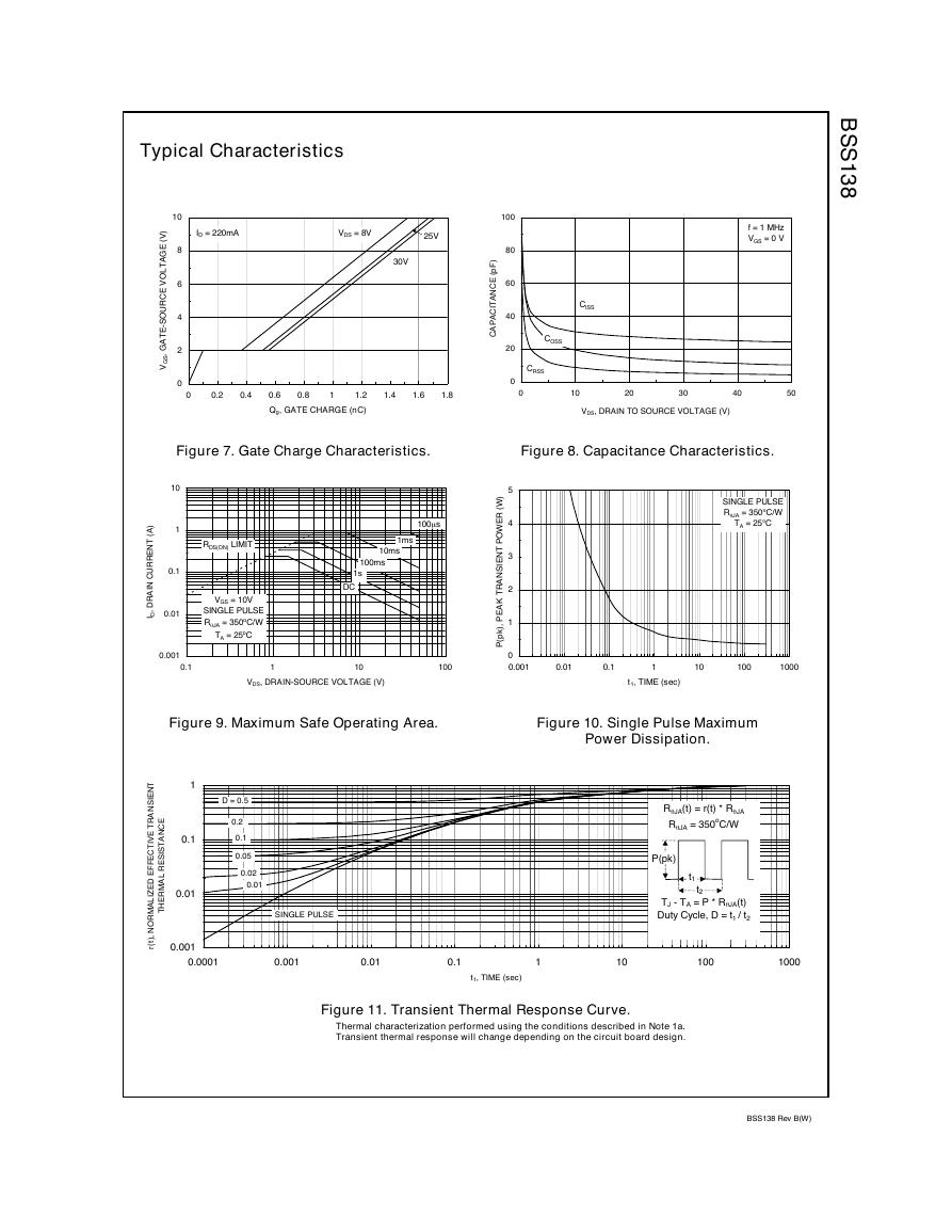
Figure 7. Gate Charge Characteristics.
Figure 8. Capacitance Characteristics.
B
S
S
1
3
8
f = 1 MHz
VGS = 0 V
100
80
60
40
20
CISS
COSS
)
F
p
(
I
E
C
N
A
T
C
A
P
A
C
)
W
(
I
R
E
W
O
P
T
N
E
S
N
A
R
T
K
A
E
P
,
)
k
p
(
P
5
4
3
2
1
0
0.001
SINGLE PULSE
RθJA = 350°C/W
TA = 25°C
0.01
0.1
1
10
100
1000
t1, TIME (sec)
Figure 10. Single Pulse Maximum
Power Dissipation.
RθJA(t) = r(t) * RθJA
RθJA = 350oC/W
P(pk)
t1
t2
TJ - TA = P * RθJA(t)
Duty Cycle, D = t1 / t2
)
A
(
T
N
E
R
R
U
C
N
A
R
D
I
,
D
I
10
1
0.1
0.01
0.001
0.1
RDS(ON) LIMIT
100µs
1ms
10ms
100ms
1s
DC
VGS = 10V
SINGLE PULSE
RθJA = 350oC/W
TA = 25oC
1
10
VDS, DRAIN-SOURCE VOLTAGE (V)
100
Figure 9. Maximum Safe Operating Area.
SINGLE PULSE
I
I
T
N
E
S
N
A
R
T
E
V
T
C
E
F
F
E
D
E
Z
L
A
M
R
O
N
I
,
)
t
(
r
I
E
C
N
A
T
S
S
E
R
L
A
M
R
E
H
T
1
0.1
0.01
D = 0.5
0.2
0.1
0.05
0.02
0.01
0.001
0.0001
0.001
0.01
0.1
1
10
100
1000
t1, TIME (sec)
Figure 11. Transient Thermal Response Curve.
Thermal characterization performed using the conditions described in Note 1a.
Transient thermal response will change depending on the circuit board design.
BSS138 Rev B(W)
�
TRADEMARKS
The following are registered and unregistered trademarks Fairchild Semiconductor owns or is authorized to use and is
not intended to be an exhaustive list of all such trademarks.
ACEx
ActiveArray
Bottomless
CoolFET
CROSSVOLT
DOME
EcoSPARK
E2CMOSTM
EnSignaTM
Across the board. Around the world.
The Power Franchise
Programmable Active Droop
DISCLAIMER
PACMAN
POP
Power247
PowerTrenchâ
QFET
QS
QT Optoelectronics
Quiet Series
RapidConfigure
RapidConnect
SILENT SWITCHERâ
SMART START
SPM
Stealth
SuperSOT-3
SuperSOT-6
SuperSOT-8
SyncFET
TinyLogic
TruTranslation
UHC
UltraFETâ
VCX
FACT
FACT Quiet Series
FASTâ
FASTr
FRFET
GlobalOptoisolator
GTO
HiSeC
I2C
ImpliedDisconnect
ISOPLANAR
LittleFET
MicroFET
MicroPak
MICROWIRE
MSX
MSXPro
OCX
OCXPro
OPTOLOGICâ
OPTOPLANAR
FAIRCHILD SEMICONDUCTOR RESERVES THE RIGHT TO MAKE CHANGES WITHOUT FURTHER
NOTICE TO ANY PRODUCTS HEREIN TO IMPROVE RELIABILITY, FUNCTION OR DESIGN. FAIRCHILD
DOES NOT ASSUME ANY LIABILITY ARISING OUT OF THE APPLICATION OR USE OF ANY PRODUCT
OR CIRCUIT DESCRIBED HEREIN; NEITHER DOES IT CONVEY ANY LICENSE UNDER ITS PATENT
RIGHTS, NOR THE RIGHTS OF OTHERS.
LIFE SUPPORT POLICY
FAIRCHILDS PRODUCTS ARE NOT AUTHORIZED FOR USE AS CRITICAL COMPONENTS IN LIFE SUPPORT
DEVICES OR SYSTEMS WITHOUT THE EXPRESS WRITTEN APPROVAL OF FAIRCHILD SEMICONDUCTOR CORPORATION.
As used herein:
1. Life support devices or systems are devices or
systems which, (a) are intended for surgical implant into
the body, or (b) support or sustain life, or (c) whose
failure to perform when properly used in accordance
with instructions for use provided in the labeling, can be
reasonably expected to result in significant injury to the
user.
PRODUCT STATUS DEFINITIONS
2. A critical component is any component of a life
support device or system whose failure to perform can
be reasonably expected to cause the failure of the life
support device or system, or to affect its safety or
effectiveness.
Definition of Terms
Datasheet Identification
Product Status
Definition
Advance Information
Formative or
In Design
Preliminary
First Production
No Identification Needed
Full Production
Obsolete
Not In Production
This datasheet contains the design specifications for
product development. Specifications may change in
any manner without notice.
This datasheet contains preliminary data, and
supplementary data will be published at a later date.
Fairchild Semiconductor reserves the right to make
changes at any time without notice in order to improve
design.
This datasheet contains final specifications. Fairchild
Semiconductor reserves the right to make changes at
any time without notice in order to improve design.
This datasheet contains specifications on a product
that has been discontinued by Fairchild semiconductor.
The datasheet is printed for reference information only.
Rev. I1
�


 V2版本原理图(Capacitive-Fingerprint-Reader-Schematic_V2).pdf
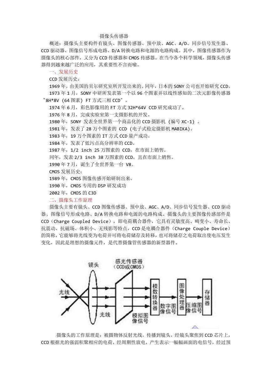 摄像头工作原理.doc
 VL53L0X简要说明(En.FLVL53L00216).pdf
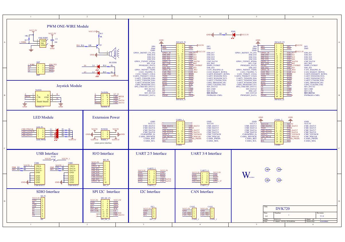 原理图(DVK720-Schematic).pdf
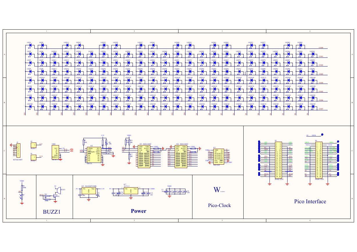 原理图(Pico-Clock-Green-Schdoc).pdf
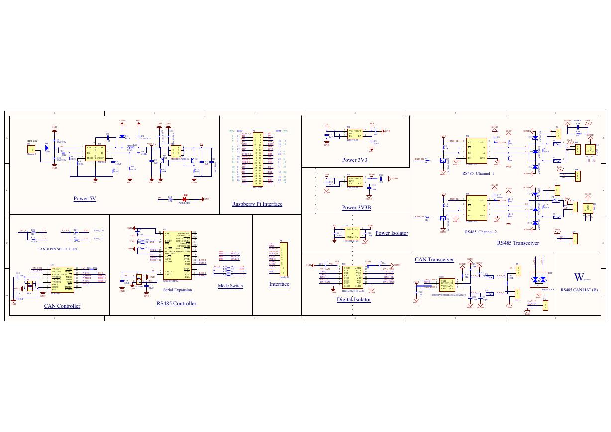 原理图(RS485-CAN-HAT-B-schematic).pdf
 File:SIM7500_SIM7600_SIM7800 Series_SSL_Application Note_V2.00.pdf
 ADS1263(Ads1262).pdf
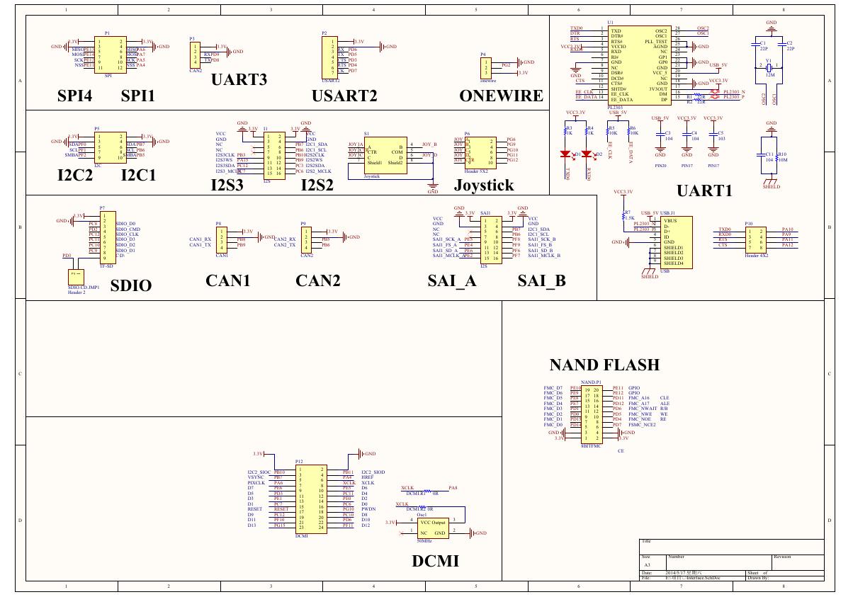 原理图(Open429Z-D-Schematic).pdf
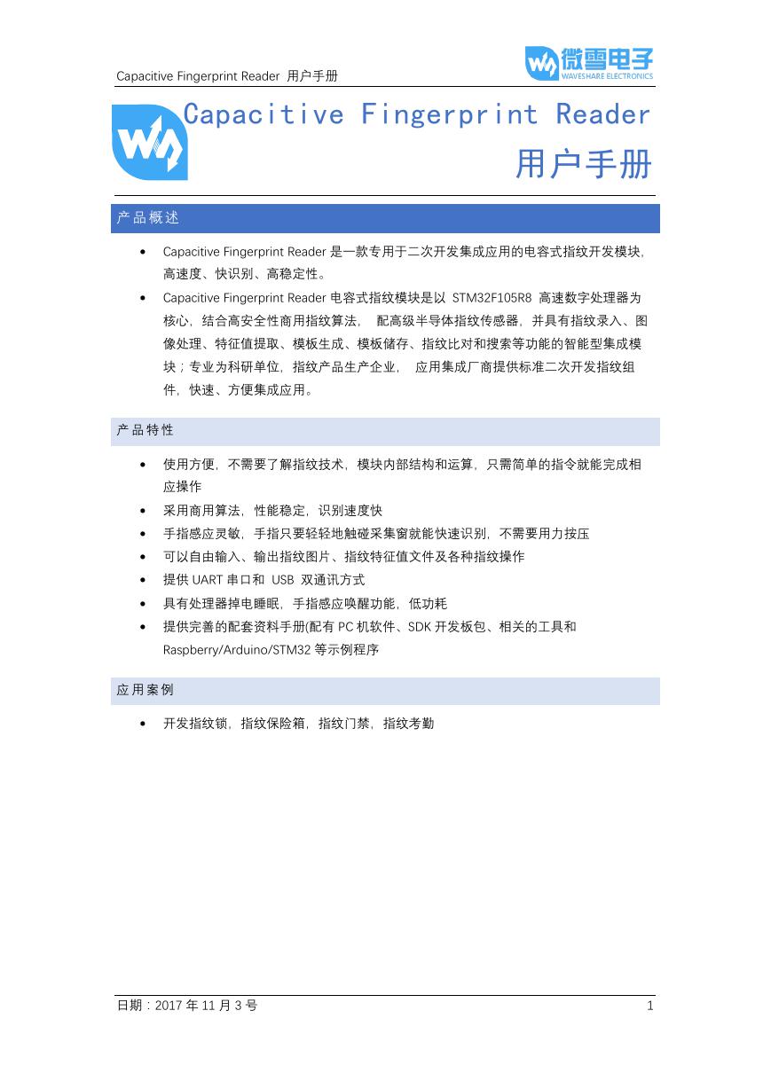 用户手册(Capacitive_Fingerprint_Reader_User_Manual_CN).pdf
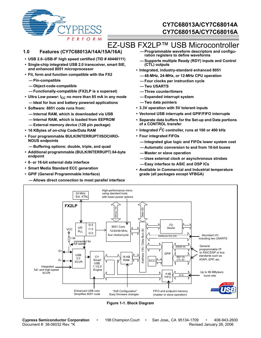 CY7C68013A(英文版)(CY7C68013A).pdf
 TechnicalReference_Dem.pdf