1 Overview
Table 1. Technical specification
1.1 VX6953CB use in a system with a hardware coprocessor
Figure 1. VX6953CB in system with processor
1.2 VX6953CB use in a system with software image processing
Figure 2. VX6953CB in a system with software image processing
1.3 Reference documents
Table 2. Reference documents
2 Device pinout
Figure 3. VX6953CB module pinout (viewed from bottom of camera module)
Table 3. Pin descriptions
3 Functional description
3.1 Analog video block
3.1.1 Block diagram
Figure 4. Overview of analog video block
3.2 Digital video block
3.2.1 Dark calibration algorithm
3.3 Device operating modes
Figure 5. System state diagram
3.3.1 Power off
3.3.2 Hardware standby
3.3.3 Software standby
3.3.4 Streaming
3.4 Power management
Table 4. Power management matrix
3.4.1 Power-up procedure
Table 5. Power-up sequence timing constraints for CCP2/CSI2 communications
Figure 6. VX6953CB power-up sequence for CCP2 mode
Figure 7. VX6953CB power-up sequence for CSI-2 mode
3.4.2 Power-down procedure
Table 6. Power-down sequence timing constraints for CSI2 communications
Figure 8. VX6953CB power-down sequence for CSI-2 mode
3.4.3 Internal power-on reset (POR)
Figure 9. POR timing
Table 7. POR cell characteristics
3.4.4 Failsafe signals
3.5 Clock and frame rate timing
3.5.1 Video frame rate control
3.5.2 PLL and clock input
Table 8. System input clock frequency range
3.5.3 Clock input type
Figure 10. Clock input types
3.6 Control and video interface formats
3.6.1 CCP serial data link
3.6.2 CSI-2 serial data link
Figure 11. CSI serial data link
3.6.3 CCI serial control bus
4 Register map
4.1 Status registers [0x0000 to 0x000F]
Table 9. Status registers [0x0000 to 0x000F]
4.2 Frame format description registers [0x0040 to 0x007F]
Table 10. Frame format description registers [0x0040 to 0x007F]
4.3 Analog gain description registers [0x0080 to 0x0097]
Table 11. Analog gain description [0x0080 to 0x0093]
4.4 Data format description registers [0x00C0 to 0x00FF]
Table 12. Data format description registers [0x00C0 to 0x00FF]
4.5 Setup registers [0x0100 to 0x01FF]
Table 13. Setup registers [0x0100 to 0x01FF]
4.6 Integration time and gain registers [0x0200 to 0x02FF]
Table 14. Integration time and gain registers [0x0200 to 0x02FF]
4.7 Video timing registers [0x0300 to 0x03FF]
Table 15. Video timing registers [0x0300 to 0x03FF]
4.8 Image scaling registers [0x0400 to 0x04FF]
Table 16. Image scaling registers [0x0400 to 0x04FF]
4.9 Image compression registers [0x0500 to 0x05FF]
Table 17. Image compression registers [0x0500 to 0x05FF]
4.10 Test pattern registers [0x0600 to 0x06FF]
Table 18. Test pattern registers [0x0600 to 0x06FF]
4.11 Fifo water mark [0x0700 to 0x0701]
Table 19. Fifo water mark registers [0x0700 to 0x0701]
4.12 DPHY [0x0810 to 0x0811]
Table 20. DPHY registers [0x0810 to 0x0811]
4.13 Binning [0x0900 to 0x0902] and [0x170C to 0x1719]
Table 21. Binning registers [0x0900 to 0x0902]
4.14 Shading correction [0x0B00]
Table 22. Shading correction registers [0x0B00]
4.15 Defect correction [0x0B05 to 0x0B09]
Table 23. Defect correction registers [0x0B05 to 0x0B09]
4.16 EDOF [0x0B80 to 0x0B8A]
Table 24. EDOF registers [0x0B80 to 0x0B8A]
4.17 Color feedback registers [0x0B8C to 0x0B95]
Table 25. Color feedback registers [0x0B8C to 0x0B95]
4.18 Integration time and gain parameter limit registers [0x1000 to 0x10FF]
Table 26. Integration time and gain parameter limit registers [0x1000 to 0x10FF]
4.19 Video timing parameter limit registers [0x1100 to 0x11FF]
Table 27. Video timing parameter limit registers [0x1100 to 0x11FF]
4.20 Image scaling parameter limit registers [0x1200 to 0x120B]
Table 28. Image scaling parameter limit registers [0x1200 to 0x120B]
4.21 Image compression parameter registers [0x1300 to 0x13FF]
Table 29. Image compression parameter limit registers [0x1300 to 0x13FF]
4.22 CSI lane mode capability [0x1600 to 0x1602]
Table 30. CSI lane mode capability registers [0x1600 - 0x1602]
4.23 Binning capability [0x1700 to 0x170B]
Table 31. Binning capability registers [0x1700 to 0x170B]
4.24 Manufacturer specific registers - Clipper 1 [0x31E8 to 0x31EB]
Table 32. Manufacturer specific registers [0x31E8 to 0x31EB]
5 Video data interface
5.1 Frame format
Figure 12. VX6953CB CCP frame format
Figure 13. VX6953CB CSI-2 frame format
6 Video timing
6.1 Output size
6.1.1 Programmable addressable region of the pixel array
Figure 14. Programmable addressable region of the pixel array
6.1.2 Programmable width and height for output image data
Figure 15. Output size within a CCP data frame
6.1.3 Scaling
Figure 16. Scaling modes
Figure 17. Scaler quality
Figure 18. Example image full scaled by a downscale factor of 2
6.1.4 Subsampling
Figure 19. Subsample readout example
6.1.5 Binning
Table 33. Binning register settings
Figure 20. Binning repair
6.2 Video timing
6.2.1 PLL block
Figure 21. VX6953CB clock relationships
6.2.2 Spread spectrum clock generator
6.2.3 Framerate
Table 34. External clock frequency examples - 5.0 Mpixel RAW10 14.5 fps (CSI-2)
Table 35. External clock frequency examples - 5.0 Mpixel RAW10 15 fps (CSI-2)
Table 36. External clock frequency examples - 5.0 Mpixel 10-8 compressed 15 fps
Table 37. Example - 5.0 Mpixel 10-8 compressed 16.65 fps (CSI-2)
Table 38. External clock frequency examples - 1080x1920 in 10-8 bit @ 30fps (CCP)
Table 39. 720x1280 @ 30 fps in RAW10 (CSI2/CCP2)
6.2.4 Derating
Figure 22. Timing block diagram
Figure 23. SMIA output timing
Figure 24. FIFO water mark control
6.3 Bayer pattern
Figure 25. Bayer pattern
6.4 Image compression
6.5 Exposure and gain control
6.5.1 Analogue gain model
Figure 26. Analogue gain register format
Table 40. Analog gain control
6.5.2 Digital gain
6.5.3 Integration and gain parameter retiming
7 Application
7.1 Schematics
Figure 27. Example of a mobile camera application (CCP2)
Figure 28. Example of a mobile camera application (CSI2)
7.2 Personality file and firmware updates
8 EDOF control
Figure 29. What is sharp?
Figure 30. EDoF main principle
8.1 EDoF capabilities
8.2 Control Interface
8.3 EDOF control registers [0x0B80 to 0x0B8A]
Table 41. EDOF registers [0x0B80 to 0x0B8A]
8.3.1 EDoF_Mode (0xB80)
8.3.2 EDoF_est_focus_distance (0x0B82)
8.3.3 EDoF tuning sliders (0xB83 to 0x0B85)
8.3.4 EDoF focus distance (0x0B88)
8.3.5 EDoF estimation control (0x0B8A)
Figure 31. Focus strategy weightings
8.4 Supermacro mode
8.5 Video modes and EDoF
8.6 EDoF and white balance
Table 42. Color feedback registers [0x0B8C to 0x0B95]
9 Image optimization
Figure 32. Processing pipe
9.1 Defect categorization
9.1.1 Pixel defects
9.1.2 Sensor array area definition
Figure 33. VX6953CB pixel defect test area
9.1.3 Pixel fault numbering convention
Figure 34. Pixel numbering notation
9.1.4 Single pixel faults
Figure 35. Single pixel fault
9.1.5 Couplet definition
Figure 36. General couplet example
9.1.6 Physical aberrations
Figure 37. Test region definition
Figure 38. Scan array for blemish
Figure 39. Fail map
Figure 40. Contiguous pixel example
9.2 Defect correction
Figure 41. Image showing defective pixels
Figure 42. Block diagram of dynamic defect correction block
Figure 43. Dynamic defect correction output example
Figure 44. Corrected Bayer pattern
9.3 Mapped couplet correction (Bruce)
9.4 Green imbalance correction
Figure 45. Green imbalance correction plots
9.5 Lens shading correction
Figure 46. Lens shading images
10 NVM contents
10.1 Green imbalance corrector
10.2 Lens shading gridiron correction
10.3 Sensitivity data
10.4 NVM map
11 EMC recommendations
12 Electrical characteristics
12.1 Operating conditions
Table 43. Operating conditions
12.2 Absolute maximum ratings
Table 44. Absolute maximum ratings
12.3 Power supply - VDIG, VANA
Table 45. Power supplies VDIG, VANA
12.3.1 Power supply (peak current) - VDIG, VANA
Table 46. In-rush current VDIG, VANA for CCP2 interface
Table 47. In-rush current VDIG, VANA for CSI-2 interface
12.3.2 Power supply ripple requirement
Table 48. Ripple requirement
12.4 System clock - EXTCLK
Table 49. System clock - EXTCLK
12.5 Power down control - XSHUTDOWN
Table 50. Power down control - XSHUTDOWN
12.6 CCI interface - SDA, SCL
12.6.1 CCI interface - DC specification
Table 51. CCI interface
12.6.2 CCI interface - timing characteristics
Table 52. CCI interface - timing characteristics
Figure 47. CCI AC characteristics
12.7 CCP interface
12.7.1 CCP interface - DC specification
Table 53. CCP interface - DC specification
12.7.2 CCP interface - timing characteristics
Table 54. CCP interface - timing characteristics
Figure 48. SubLVDS AC timing
12.8 CSI-2 interface
12.8.1 CSI-2 interface - DC specification
Table 55. CSI-2 interface - high speed mode - DC specification
Table 56. CSI-2 interface - low power mode - DC specification
12.8.2 CSI-2 interface - AC specification
Table 57. CSI-2 interface - high speed mode - AC specification
Table 58. CSI-2 interface - low power mode - AC specification
13 Optical specification
13.1 Lens characteristics
Table 59. Typical lens design characteristics for first source lens supplier
13.2 Text, 1D and 2D codes reading
Figure 49. Barcode and QR code examples
Table 60. QR code (2D)resolution reading capability
14 Mechanical
14.1 Packaging and delivery
Figure 50. Marking diagram
Table 61. Substrate marking codification
14.2 Inner box labelling
14.3 Packing
14.4 Module outline
Table 62. Outline drawing information
15 Ordering information
Table 63. Device summary
16 User precaution
17 Acronyms and abbreviations
Table 64. Acronyms and abbreviations
18 Revision history
Table 65. Document revision history





 V2版本原理图(Capacitive-Fingerprint-Reader-Schematic_V2).pdf
 摄像头工作原理.doc
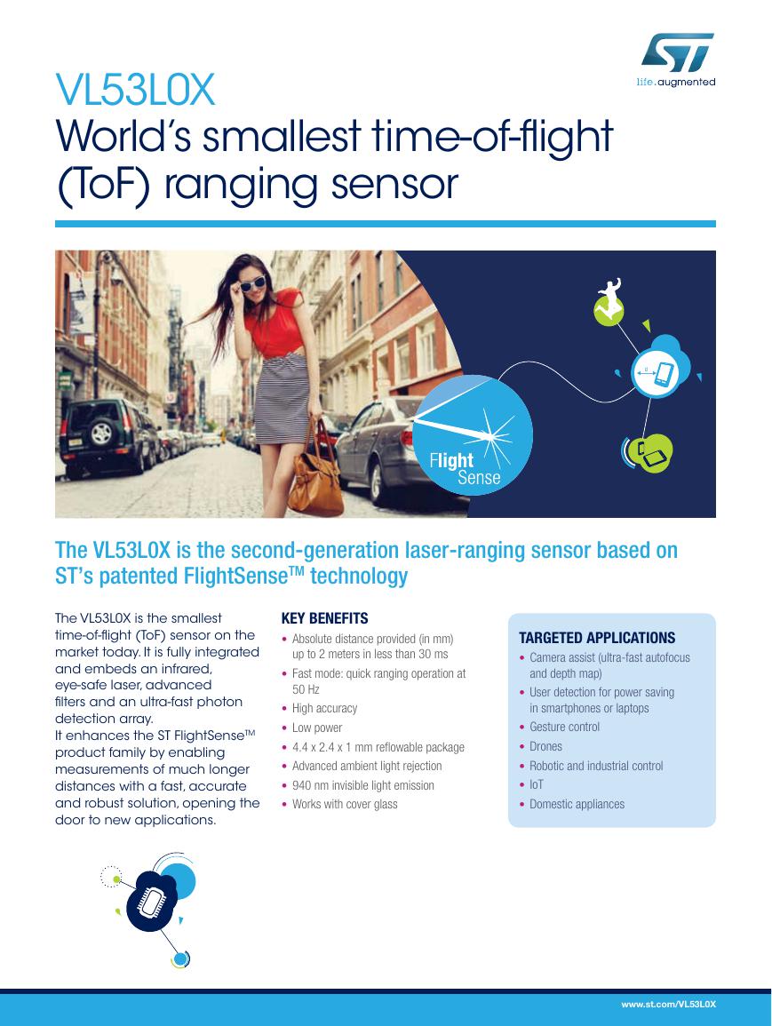 VL53L0X简要说明(En.FLVL53L00216).pdf
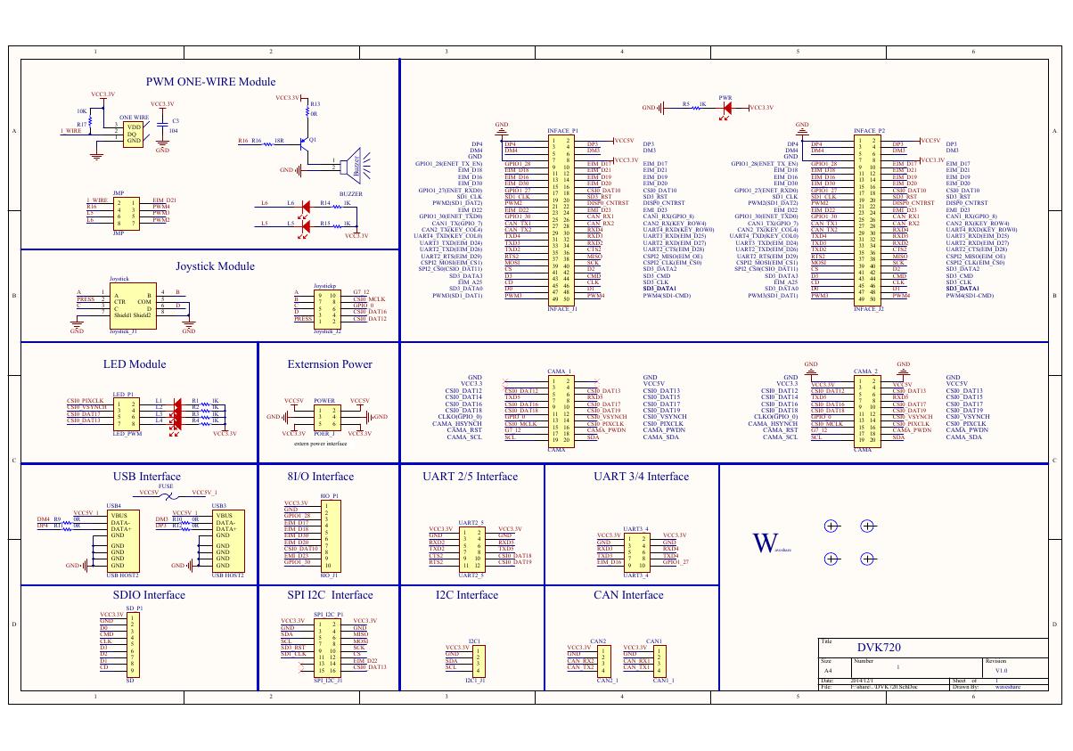 原理图(DVK720-Schematic).pdf
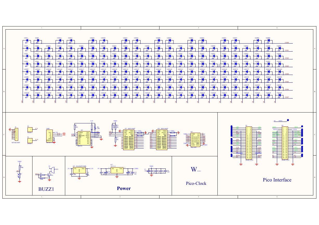 原理图(Pico-Clock-Green-Schdoc).pdf
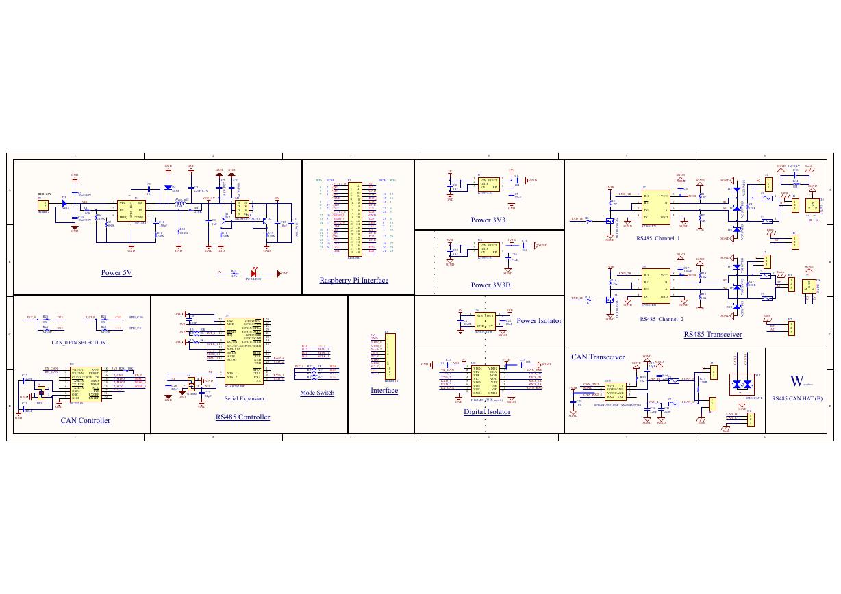 原理图(RS485-CAN-HAT-B-schematic).pdf
 File:SIM7500_SIM7600_SIM7800 Series_SSL_Application Note_V2.00.pdf
 ADS1263(Ads1262).pdf
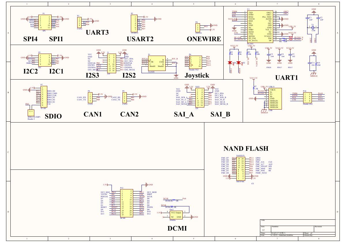 原理图(Open429Z-D-Schematic).pdf
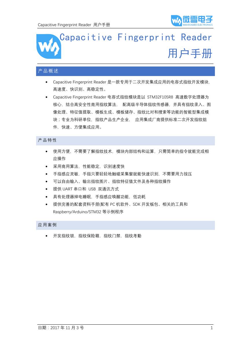 用户手册(Capacitive_Fingerprint_Reader_User_Manual_CN).pdf
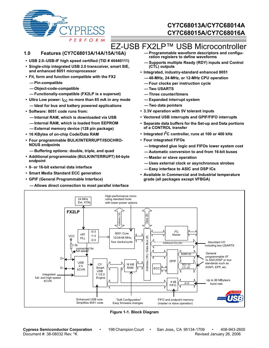 CY7C68013A(英文版)(CY7C68013A).pdf
 TechnicalReference_Dem.pdf