logo资料库

NRF51822_PS_v3.1(NRF51822_PS_v3.1).pdf

第1页 / 共115页
第2页 / 共115页
第3页 / 共115页
第4页 / 共115页
第5页 / 共115页
第6页 / 共115页
第7页 / 共115页
第8页 / 共115页
资料共115页,剩余部分请下载后查看
1 Introduction
1.1 Required reading
1.2 Writing conventions
2 Product overview
2.1 Block diagram
2.2 Pin assignments and functions
2.2.1 Pin assignment QFN48
2.2.2 CDAB WLCSP ball assignment and functions
2.2.3 CEAA and CFAC WLCSP ball assignment and functions
3 System blocks
3.1 CPU
3.2 Memory
3.2.1 Code organization
3.2.2 RAM organization
3.3 Memory Protection Unit (MPU)
3.4 Power management (POWER)
3.4.1 Power supply
3.4.2 Power management
3.5 Programmable Peripheral Interconnect (PPI)
3.6 Clock management (CLOCK)
3.6.1 16/32 MHz crystal oscillator
3.6.2 32.768 kHz crystal oscillator
3.6.3 32.768 kHz RC oscillator
3.6.4 Synthesized 32.768 kHz clock
3.7 GPIO
3.8 Debugger support
4 Peripheral blocks
4.1 2.4 GHz radio (RADIO)
4.2 Timer/counters (TIMER)
4.3 Real Time Counter (RTC)
4.4 AES Electronic Codebook Mode Encryption (ECB)
4.5 AES CCM Mode Encryption (CCM)
4.6 Accelerated Address Resolver (AAR)
4.7 Random Number Generator (RNG)
4.8 Watchdog Timer (WDT)
4.9 Temperature sensor (TEMP)
4.10 Serial Peripheral Interface (SPI/SPIS)
4.11 Two-wire interface (TWI)
4.12 Universal Asynchronous Receiver/Transmitter (UART)
4.13 Quadrature Decoder (QDEC)
4.14 Analog to Digital Converter (ADC)
4.15 GPIO Task Event blocks (GPIOTE)
4.16 Low Power Comparator (LPCOMP)
5 Instance table
6 Absolute maximum ratings
7 Operating conditions
7.1 WLCSP light sensitivity
8 Electrical specifications
8.1 Clock sources
8.1.1 16/32 MHz crystal startup
8.1.2 16 MHz crystal oscillator (16M XOSC)
8.1.3 32 MHz crystal oscillator (32M XOSC)
8.1.4 16 MHz RC oscillator (16M RCOSC)
8.1.5 32.768 kHz crystal oscillator (32k XOSC)
8.1.6 32.768 kHz RC oscillator (32k RCOSC)
8.1.7 32.768 kHz Synthesized oscillator (32k SYNT)
8.2 Power management
8.3 Block resource requirements
8.4 CPU
8.5 Radio transceiver
8.5.1 General radio characteristics
8.5.2 Radio current consumption with DC/DC disabled
8.5.3 Radio current consumption with DC/DC enabled
8.5.4 Transmitter specifications
8.5.5 Receiver specifications
8.5.6 Radio timing parameters
8.5.7 Antenna matching network requirements
8.6 Received Signal Strength Indicator (RSSI) specifications
8.7 Universal Asynchronous Receiver/Transmitter (UART) specifications
8.8 Serial Peripheral Interface Slave (SPIS) specifications
8.9 Serial Peripheral Interface (SPI) Master specifications
8.10 I2C compatible Two Wire Interface (TWI) specifications
8.11 GPIO Tasks and Events (GPIOTE) specifications
8.12 Analog to Digital Converter (ADC) specifications
8.13 Timer (TIMER) specifications
8.14 Real Time Counter (RTC)
8.15 Temperature sensor (TEMP)
8.16 Random Number Generator (RNG) specifications
8.17 AES Electronic Codebook Mode Encryption (ECB) specifications
8.18 AES CCM Mode Encryption (CCM) specifications
8.19 Accelerated Address Resolver (AAR) specifications
8.20 Watchdog Timer (WDT) specifications
8.21 Quadrature Decoder (QDEC) specifications
8.22 Non-Volatile Memory Controller (NVMC) specifications
8.23 General Purpose I/O (GPIO) specifications
8.24 Low Power Comparator (LPCOMP) specifications
9 Mechanical specifications
9.1 QFN48 package
9.2 CDAB WLCSP package
9.3 CEAA WLCSP package
9.4 CFAC WLCSP package
10 Ordering information
10.1 Chip marking
10.2 Inner box label
10.3 Outer box label
10.4 Order code
10.5 Abbreviations
10.6 Code ranges and values
10.7 Product options
10.7.1 nRF ICs
10.7.2 Development tools
11 Reference circuitry
11.1 PCB guidelines
11.1.1 PCB layout example
11.2 Reference design schematics
11.3 QFAA QFN48 package
11.3.1 QFAA QFN48 schematic with internal LDO setup
11.3.2 QFAA QFN48 schematic with low voltage mode setup
11.3.3 QFAA QFN48 schematic with DC/DC converter setup
11.4 QFAB QFN48 package
11.4.1 QFAB QFN48 schematic with internal LDO setup
11.4.2 QFAB QFN48 schematic with low voltage mode setup
11.4.3 QFAB QFN48 schematic with DC/DC converter setup
11.5 QFAC QFN48 package
11.5.1 QFAC QFN48 schematic with internal LDO setup
11.5.2 QFAC QFN48 schematic with low voltage mode setup
11.5.3 QFAC QFN48 schematic with DC/DC converter setup
11.6 CDAB WLCSP package
11.6.1 CDAB WLCSP schematic with internal LDO setup
11.6.2 CDAB WLCSP schematic with low voltage mode setup
11.6.3 CDAB WLCSP schematic with DC/DC converter setup
11.7 CEAA WLCSP package
11.7.1 CEAA WLCSP schematic with internal LDO setup
11.7.2 CEAA WLCSP schematic with low voltage mode setup
11.7.3 CEAA WLCSP schematic with DC/DC converter setup
11.8 CFAC WLCSP package
11.8.1 CFAC WLCSP schematic with internal LDO setup
11.8.2 CFAC WLCSP schematic with low voltage mode setup
11.8.3 CFAC WLCSP schematic with DC/DC converter setup
12 Glossary
nRF51822 Multiprotocol Bluetooth® low energy/2.4 GHz RF System on Chip Product Specification v3.1 Key Features Applications • Computer peripherals and I/O devices • Mouse • Keyboard • Multi-touch trackpad • Interactive entertainment devices • Remote control • Gaming controller • Beacons • Personal Area Networks • Health/fitness sensor and monitor devices • Medical devices • Key-fobs + wrist watches • Remote control toys • 2.4 GHz transceiver -93 dBm sensitivity in Bluetooth® low energy mode • • 250 kbps, 1 Mbps, 2 Mbps supported data rates • TX Power -20 to +4 dBm in 4 dB steps • TX Power -30 dBm Whisper mode • 13 mA peak RX, 10.5 mA peak TX (0 dBm) • 9.7 mA peak RX, 8 mA peak TX (0 dBm) with DC/DC • RSSI (1 dB resolution) • ARM® Cortex™-M0 32 bit processor • 275 μA/MHz running from flash memory • 150 μA/MHz running from RAM • Serial Wire Debug (SWD) • S100 series SoftDevice ready • Memory • 256 kB or 128 kB embedded flash program memory • 16 kB or 32 kB RAM • On-air compatibility with nRF24L series • Flexible Power Management • Supply voltage range 1.8 V to 3.6 V • 4.2 μs wake-up using 16 MHz RCOSC • 0.6 μA at 3 V OFF mode • 1.2 μA at 3 V in OFF mode + 1 region RAM retention • 2.6 μA at 3 V ON mode, all blocks IDLE • 8/9/10 bit ADC - 8 configurable channels • 31 General Purpose I/O Pins • One 32 bit and two 16 bit timers with counter mode • SPI Master/Slave • Low power comparator • Temperature sensor • Two-wire Master (I2C compatible) • UART (CTS/RTS) • CPU independent Programmable Peripheral Interconnect (PPI) • Quadrature Decoder (QDEC) • AES HW encryption • Real Timer Counter (RTC) • Package variants • QFN48 package, 6 x 6 mm • WLCSP package, 3.50 x 3.83 mm • WLCSP package, 3.83 x 3.83 mm • WLCSP package, 3.50 x 3.33 mm Reproduction in whole or in part is prohibited without the prior written permission of the copyright holder. Copyright © 2014 Nordic Semiconductor ASA. All rights reserved.
nRF51822 Product Specification v3.1 Liability disclaimer Nordic Semiconductor ASA reserves the right to make changes without further notice to the product to improve reliability, function or design. Nordic Semiconductor ASA does not assume any liability arising out of the application or use of any product or circuits described herein. Life support applications Nordic Semiconductor’s products are not designed for use in life support appliances, devices, or systems where malfunction of these products can reasonably be expected to result in personal injury. Nordic Semiconductor ASA customers using or selling these products for use in such applications do so at their own risk and agree to fully indemnify Nordic Semiconductor ASA for any damages resulting from such improper use or sale. Contact details For your nearest distributor, please visit www.nordicsemi.com. Information regarding product updates, downloads, and technical support can be accessed through your My Page account on our home page. Main office: Otto Nielsens veg 12 7052 Trondheim Norway Phone: +47 72 89 89 00 Fax: +47 72 89 89 89 Mailing address: Nordic Semiconductor P.O. Box 2336 7004 Trondheim Norway RoHS and REACH statement Nordic Semiconductor's products meet the requirements of Directive 2002/95/EC of the European Parliament and of the Council on the Restriction of Hazardous Substances (RoHS) and the requirements of the REACH regulation (EC 1907/2006) on Registration, Evaluation, Authorization and Restriction of Chemicals. The SVHC (Substances of Very High Concern) candidate list is continually being updated. Complete hazardous substance reports, material composition reports and latest version of Nordic's REACH statement can be found on our website www.nordicsemi.com. Page 2
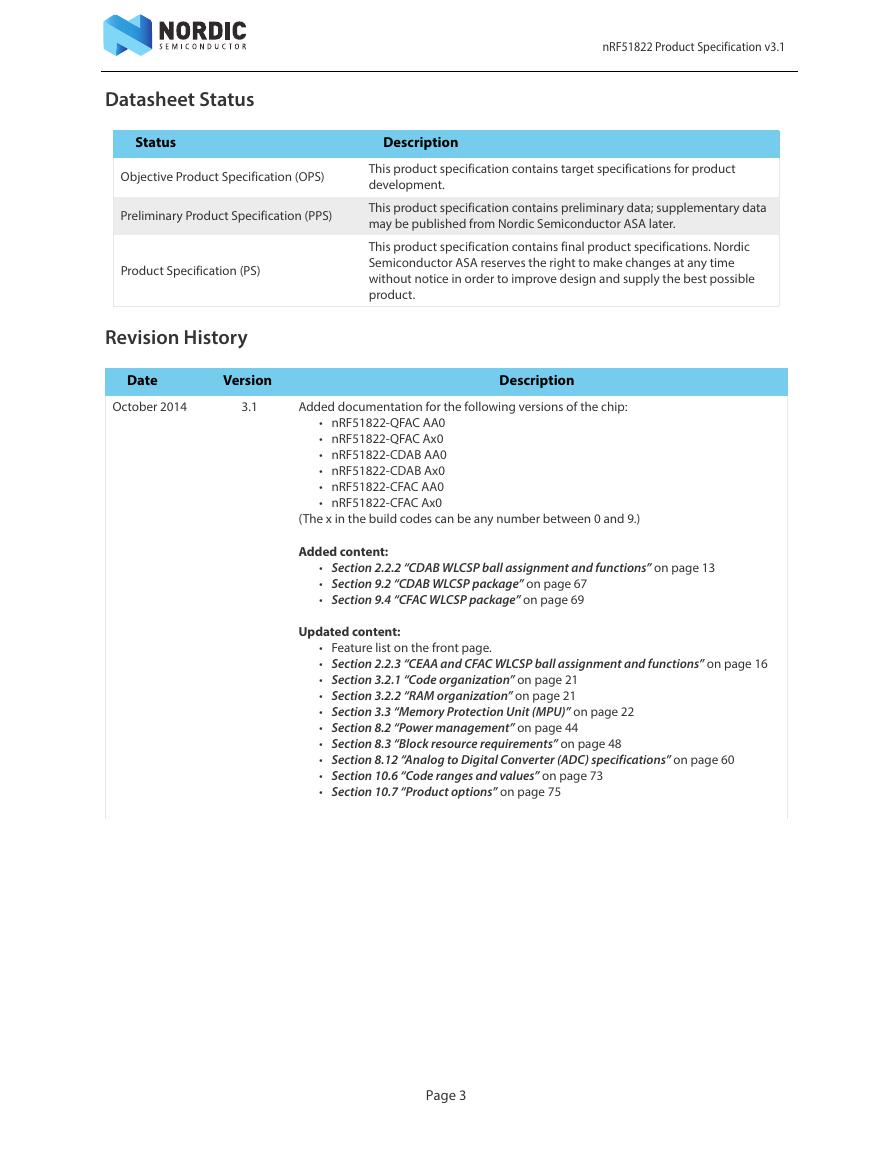
nRF51822 Product Specification v3.1 Datasheet Status Status Description Objective Product Specification (OPS) Preliminary Product Specification (PPS) Product Specification (PS) Revision History This product specification contains target specifications for product development. This product specification contains preliminary data; supplementary data may be published from Nordic Semiconductor ASA later. This product specification contains final product specifications. Nordic Semiconductor ASA reserves the right to make changes at any time without notice in order to improve design and supply the best possible product. Date Version Description October 2014 3.1 Added documentation for the following versions of the chip: • nRF51822-QFAC AA0 • nRF51822-QFAC Ax0 • nRF51822-CDAB AA0 • nRF51822-CDAB Ax0 • nRF51822-CFAC AA0 • nRF51822-CFAC Ax0 (The x in the build codes can be any number between 0 and 9.) Added content: • Section 2.2.2 “CDAB WLCSP ball assignment and functions” on page 13 • Section 9.2 “CDAB WLCSP package” on page 67 • Section 9.4 “CFAC WLCSP package” on page 69 Updated content: • Feature list on the front page. • Section 2.2.3 “CEAA and CFAC WLCSP ball assignment and functions” on page 16 • Section 3.2.1 “Code organization” on page 21 • Section 3.2.2 “RAM organization” on page 21 • Section 3.3 “Memory Protection Unit (MPU)” on page 22 • Section 8.2 “Power management” on page 44 • Section 8.3 “Block resource requirements” on page 48 • Section 8.12 “Analog to Digital Converter (ADC) specifications” on page 60 • Section 10.6 “Code ranges and values” on page 73 • Section 10.7 “Product options” on page 75 Page 3
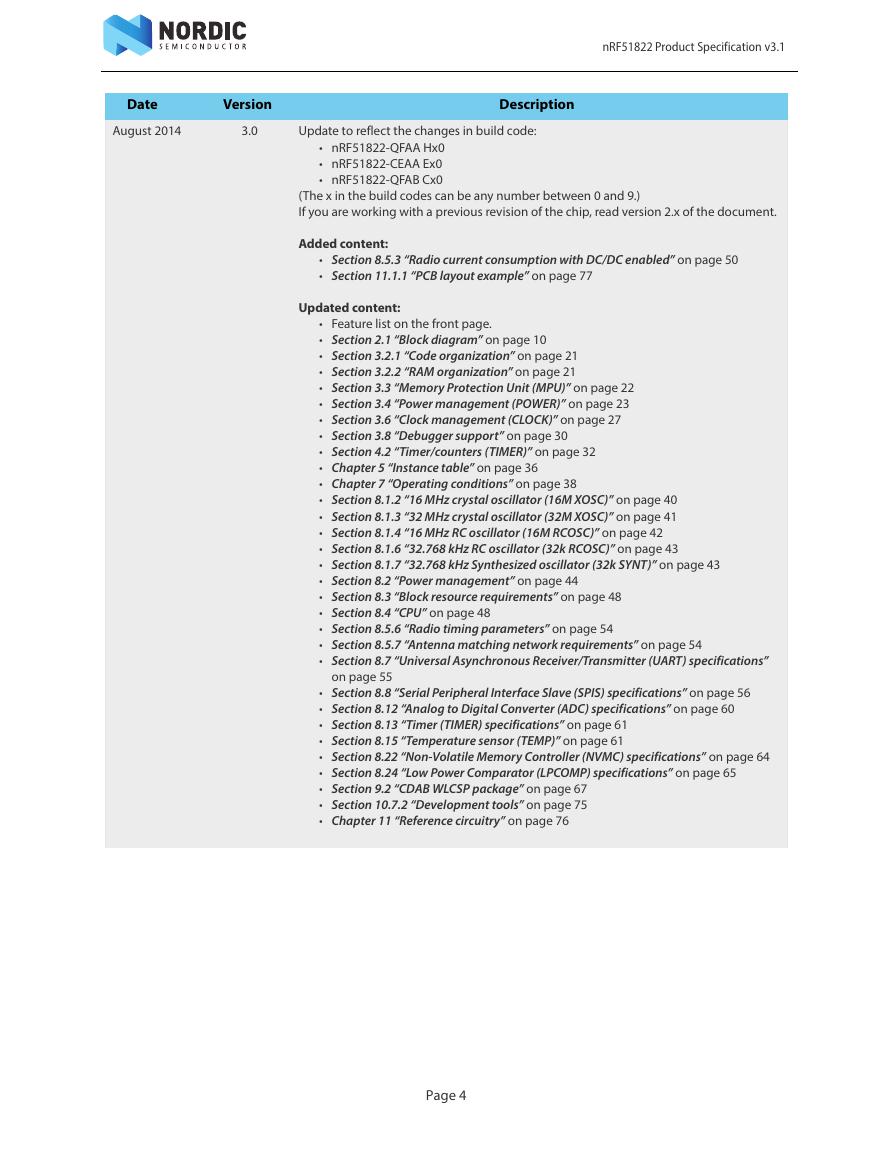
nRF51822 Product Specification v3.1 Date Version Description August 2014 3.0 Update to reflect the changes in build code: • nRF51822-QFAA Hx0 • nRF51822-CEAA Ex0 • nRF51822-QFAB Cx0 (The x in the build codes can be any number between 0 and 9.) If you are working with a previous revision of the chip, read version 2.x of the document. Added content: • Section 8.5.3 “Radio current consumption with DC/DC enabled” on page 50 • Section 11.1.1 “PCB layout example” on page 77 Updated content: • Feature list on the front page. • Section 2.1 “Block diagram” on page 10 • Section 3.2.1 “Code organization” on page 21 • Section 3.2.2 “RAM organization” on page 21 • Section 3.3 “Memory Protection Unit (MPU)” on page 22 • Section 3.4 “Power management (POWER)” on page 23 • Section 3.6 “Clock management (CLOCK)” on page 27 • Section 3.8 “Debugger support” on page 30 • Section 4.2 “Timer/counters (TIMER)” on page 32 • Chapter 5 “Instance table” on page 36 • Chapter 7 “Operating conditions” on page 38 • Section 8.1.2 “16 MHz crystal oscillator (16M XOSC)” on page 40 • Section 8.1.3 “32 MHz crystal oscillator (32M XOSC)” on page 41 • Section 8.1.4 “16 MHz RC oscillator (16M RCOSC)” on page 42 • Section 8.1.6 “32.768 kHz RC oscillator (32k RCOSC)” on page 43 • Section 8.1.7 “32.768 kHz Synthesized oscillator (32k SYNT)” on page 43 • Section 8.2 “Power management” on page 44 • Section 8.3 “Block resource requirements” on page 48 • Section 8.4 “CPU” on page 48 • Section 8.5.6 “Radio timing parameters” on page 54 • Section 8.5.7 “Antenna matching network requirements” on page 54 • Section 8.7 “Universal Asynchronous Receiver/Transmitter (UART) specifications” on page 55 • Section 8.8 “Serial Peripheral Interface Slave (SPIS) specifications” on page 56 • Section 8.12 “Analog to Digital Converter (ADC) specifications” on page 60 • Section 8.13 “Timer (TIMER) specifications” on page 61 • Section 8.15 “Temperature sensor (TEMP)” on page 61 • Section 8.22 “Non-Volatile Memory Controller (NVMC) specifications” on page 64 • Section 8.24 “Low Power Comparator (LPCOMP) specifications” on page 65 • Section 9.2 “CDAB WLCSP package” on page 67 • Section 10.7.2 “Development tools” on page 75 • Chapter 11 “Reference circuitry” on page 76 Page 4
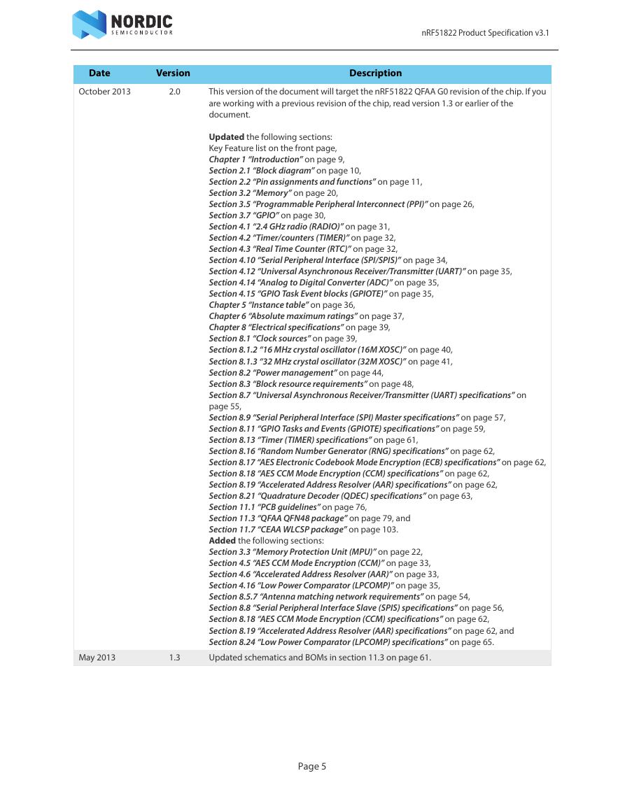
Date Version October 2013 2.0 May 2013 1.3 nRF51822 Product Specification v3.1 Description This version of the document will target the nRF51822 QFAA G0 revision of the chip. If you are working with a previous revision of the chip, read version 1.3 or earlier of the document. Updated the following sections: Key Feature list on the front page, Chapter 1 “Introduction” on page 9, Section 2.1 “Block diagram” on page 10, Section 2.2 “Pin assignments and functions” on page 11, Section 3.2 “Memory” on page 20, Section 3.5 “Programmable Peripheral Interconnect (PPI)” on page 26, Section 3.7 “GPIO” on page 30, Section 4.1 “2.4 GHz radio (RADIO)” on page 31, Section 4.2 “Timer/counters (TIMER)” on page 32, Section 4.3 “Real Time Counter (RTC)” on page 32, Section 4.10 “Serial Peripheral Interface (SPI/SPIS)” on page 34, Section 4.12 “Universal Asynchronous Receiver/Transmitter (UART)” on page 35, Section 4.14 “Analog to Digital Converter (ADC)” on page 35, Section 4.15 “GPIO Task Event blocks (GPIOTE)” on page 35, Chapter 5 “Instance table” on page 36, Chapter 6 “Absolute maximum ratings” on page 37, Chapter 8 “Electrical specifications” on page 39, Section 8.1 “Clock sources” on page 39, Section 8.1.2 “16 MHz crystal oscillator (16M XOSC)” on page 40, Section 8.1.3 “32 MHz crystal oscillator (32M XOSC)” on page 41, Section 8.2 “Power management” on page 44, Section 8.3 “Block resource requirements” on page 48, Section 8.7 “Universal Asynchronous Receiver/Transmitter (UART) specifications” on page 55, Section 8.9 “Serial Peripheral Interface (SPI) Master specifications” on page 57, Section 8.11 “GPIO Tasks and Events (GPIOTE) specifications” on page 59, Section 8.13 “Timer (TIMER) specifications” on page 61, Section 8.16 “Random Number Generator (RNG) specifications” on page 62, Section 8.17 “AES Electronic Codebook Mode Encryption (ECB) specifications” on page 62, Section 8.18 “AES CCM Mode Encryption (CCM) specifications” on page 62, Section 8.19 “Accelerated Address Resolver (AAR) specifications” on page 62, Section 8.21 “Quadrature Decoder (QDEC) specifications” on page 63, Section 11.1 “PCB guidelines” on page 76, Section 11.3 “QFAA QFN48 package” on page 79, and Section 11.7 “CEAA WLCSP package” on page 103. Added the following sections: Section 3.3 “Memory Protection Unit (MPU)” on page 22, Section 4.5 “AES CCM Mode Encryption (CCM)” on page 33, Section 4.6 “Accelerated Address Resolver (AAR)” on page 33, Section 4.16 “Low Power Comparator (LPCOMP)” on page 35, Section 8.5.7 “Antenna matching network requirements” on page 54, Section 8.8 “Serial Peripheral Interface Slave (SPIS) specifications” on page 56, Section 8.18 “AES CCM Mode Encryption (CCM) specifications” on page 62, Section 8.19 “Accelerated Address Resolver (AAR) specifications” on page 62, and Section 8.24 “Low Power Comparator (LPCOMP) specifications” on page 65. Updated schematics and BOMs in section 11.3 on page 61. Page 5
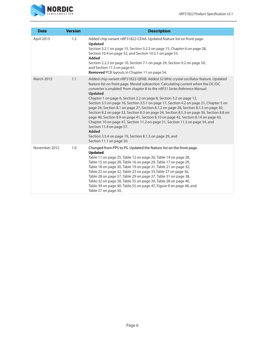
Date April 2013 Version 1.2 March 2013 1.1 November 2012 1.0 nRF51822 Product Specification v3.1 Description Added chip variant nRF51822-CEAA. Updated feature list on front page. Updated Section 3.2.1 on page 15, Section 3.2.2 on page 15, Chapter 6 on page 28, Section 10.4 on page 52, and Section 10.5.1 on page 53. Added Section 2.2.2 on page 10, Section 7.1 on page 29, Section 9.2 on page 50, and Section 11.3 on page 61. Removed PCB layouts in Chapter 11 on page 54. Added chip variant nRF51822-QFAB. Added 32 MHz crystal oscillator feature. Updated feature list on front page. Moved subsection ‘Calculating current when the DC/DC converter is enabled’ from chapter 8 to the nRF51 Series Reference Manual. Updated Chapter 1 on page 6, Section 2.2 on page 8, Section 3.2 on page 12, Section 3.5 on page 16, Section 3.5.1 on page 17, Section 4.2 on page 21, Chapter 5 on page 24, Section 8.1 on page 27, Section 8.1.2 on page 28, Section 8.1.5 on page 30, Section 8.2 on page 32, Section 8.3 on page 34, Section 8.5.3 on page 36, Section 8.8 on page 40, Section 8.9 on page 41, Section 8.10 on page 42, Section 8.14 on page 43, Chapter 10 on page 47, Section 11.2 on page 51, Section 11.3 on page 54, and Section 11.4 on page 57. Added Section 3.5.4 on page 19, Section 8.1.3 on page 29, and Section 11.1 on page 50. Changed from PPS to PS. Updated the feature list on the front page. Updated Table 11 on page 25, Table 12 on page 26, Table 14 on page 28, Table 15 on page 28, Table 16 on page 29, Table 17 on page 29, Table 18 on page 30, Table 19 on page 31, Table 21 on page 32, Table 22 on page 32, Table 23 on page 33,Table 27 on page 36, Table 28 on page 37, Table 29 on page 37, Table 31 on page 38, Table 32 on page 38, Table 35 on page 39, Table 38 on page 40, Table 39 on page 40, Table 55 on page 47, Figure 9 on page 48, and Table 57 on page 50. Page 6
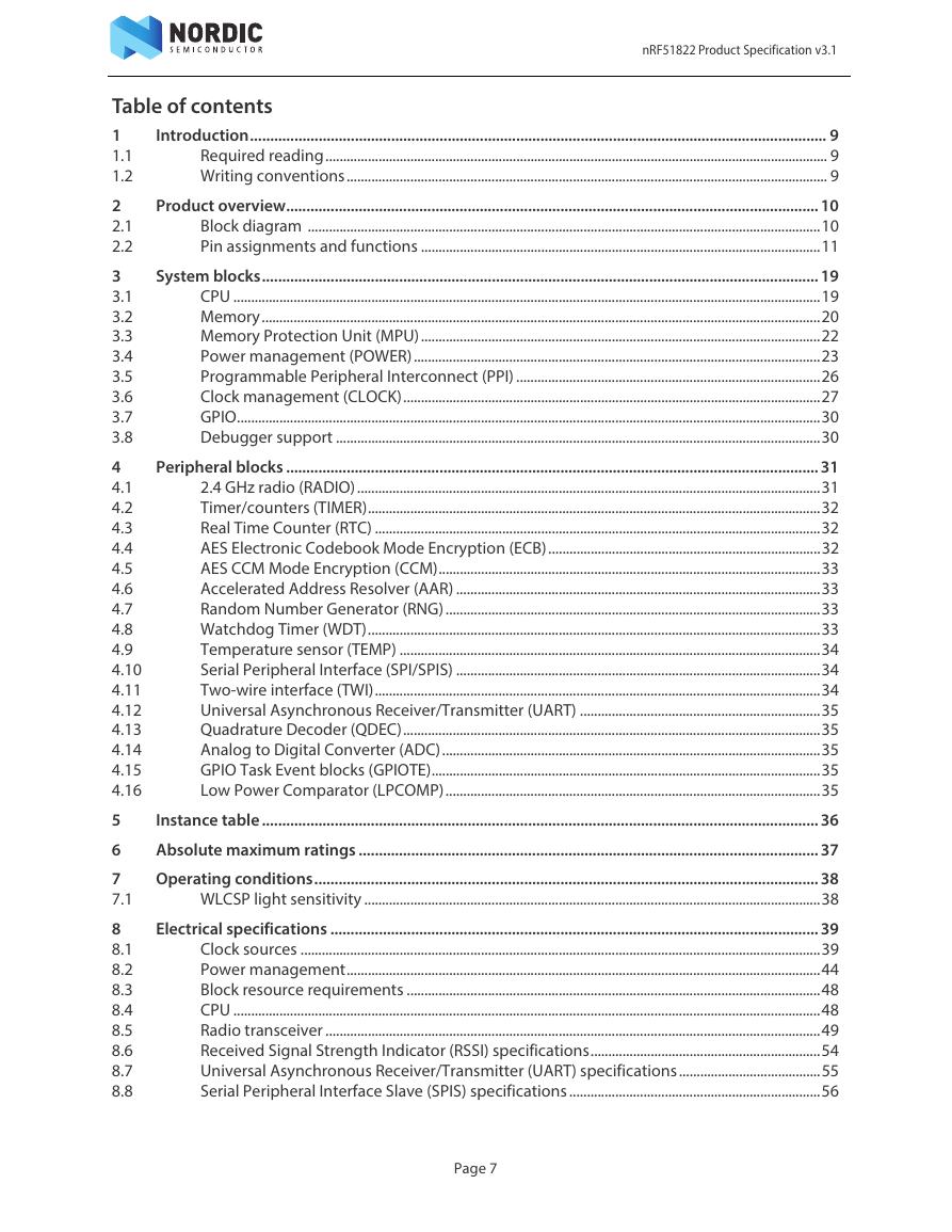
nRF51822 Product Specification v3.1 Table of contents 1 1.1 1.2 2 2.1 2.2 3 3.1 3.2 3.3 3.4 3.5 3.6 3.7 3.8 4 4.1 4.2 4.3 4.4 4.5 4.6 4.7 4.8 4.9 4.10 4.11 4.12 4.13 4.14 4.15 4.16 5 6 7 7.1 8 8.1 8.2 8.3 8.4 8.5 8.6 8.7 8.8 Introduction............................................................................................................................................... 9 Required reading.............................................................................................................................................. 9 Writing conventions........................................................................................................................................ 9 Product overview.................................................................................................................................... 10 Block diagram .................................................................................................................................................10 Pin assignments and functions .................................................................................................................11 System blocks.......................................................................................................................................... 19 CPU ......................................................................................................................................................................19 Memory..............................................................................................................................................................20 Memory Protection Unit (MPU).................................................................................................................22 Power management (POWER)...................................................................................................................23 Programmable Peripheral Interconnect (PPI) ......................................................................................26 Clock management (CLOCK)......................................................................................................................27 GPIO.....................................................................................................................................................................30 Debugger support .........................................................................................................................................30 Peripheral blocks .................................................................................................................................... 31 2.4 GHz radio (RADIO)...................................................................................................................................31 Timer/counters (TIMER)................................................................................................................................32 Real Time Counter (RTC) ..............................................................................................................................32 AES Electronic Codebook Mode Encryption (ECB).............................................................................32 AES CCM Mode Encryption (CCM)............................................................................................................33 Accelerated Address Resolver (AAR) .......................................................................................................33 Random Number Generator (RNG)..........................................................................................................33 Watchdog Timer (WDT)................................................................................................................................33 Temperature sensor (TEMP) .......................................................................................................................34 Serial Peripheral Interface (SPI/SPIS) .......................................................................................................34 Two-wire interface (TWI)..............................................................................................................................34 Universal Asynchronous Receiver/Transmitter (UART) ....................................................................35 Quadrature Decoder (QDEC)......................................................................................................................35 Analog to Digital Converter (ADC)...........................................................................................................35 GPIO Task Event blocks (GPIOTE)..............................................................................................................35 Low Power Comparator (LPCOMP)..........................................................................................................35 Instance table .......................................................................................................................................... 36 Absolute maximum ratings .................................................................................................................. 37 Operating conditions............................................................................................................................. 38 WLCSP light sensitivity .................................................................................................................................38 Electrical specifications ......................................................................................................................... 39 Clock sources ...................................................................................................................................................39 Power management......................................................................................................................................44 Block resource requirements .....................................................................................................................48 CPU ......................................................................................................................................................................48 Radio transceiver ............................................................................................................................................49 Received Signal Strength Indicator (RSSI) specifications.................................................................54 Universal Asynchronous Receiver/Transmitter (UART) specifications........................................55 Serial Peripheral Interface Slave (SPIS) specifications .......................................................................56 Page 7
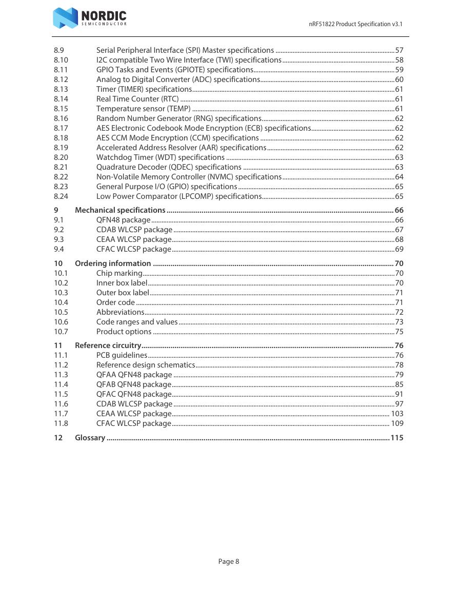
nRF51822 Product Specification v3.1 8.9 8.10 8.11 8.12 8.13 8.14 8.15 8.16 8.17 8.18 8.19 8.20 8.21 8.22 8.23 8.24 9 9.1 9.2 9.3 9.4 10 10.1 10.2 10.3 10.4 10.5 10.6 10.7 11 11.1 11.2 11.3 11.4 11.5 11.6 11.7 11.8 12 Serial Peripheral Interface (SPI) Master specifications ......................................................................57 I2C compatible Two Wire Interface (TWI) specifications..................................................................58 GPIO Tasks and Events (GPIOTE) specifications...................................................................................59 Analog to Digital Converter (ADC) specifications...............................................................................60 Timer (TIMER) specifications.......................................................................................................................61 Real Time Counter (RTC) ..............................................................................................................................61 Temperature sensor (TEMP) .......................................................................................................................61 Random Number Generator (RNG) specifications..............................................................................62 AES Electronic Codebook Mode Encryption (ECB) specifications.................................................62 AES CCM Mode Encryption (CCM) specifications ...............................................................................62 Accelerated Address Resolver (AAR) specifications...........................................................................62 Watchdog Timer (WDT) specifications ...................................................................................................63 Quadrature Decoder (QDEC) specifications .........................................................................................63 Non-Volatile Memory Controller (NVMC) specifications..................................................................64 General Purpose I/O (GPIO) specifications............................................................................................65 Low Power Comparator (LPCOMP) specifications..............................................................................65 Mechanical specifications ..................................................................................................................... 66 QFN48 package...............................................................................................................................................66 CDAB WLCSP package..................................................................................................................................67 CEAA WLCSP package...................................................................................................................................68 CFAC WLCSP package...................................................................................................................................69 Ordering information ............................................................................................................................ 70 Chip marking....................................................................................................................................................70 Inner box label.................................................................................................................................................70 Outer box label................................................................................................................................................71 Order code ........................................................................................................................................................71 Abbreviations...................................................................................................................................................72 Code ranges and values...............................................................................................................................73 Product options ..............................................................................................................................................75 Reference circuitry.................................................................................................................................. 76 PCB guidelines.................................................................................................................................................76 Reference design schematics.....................................................................................................................78 QFAA QFN48 package ..................................................................................................................................79 QFAB QFN48 package...................................................................................................................................85 QFAC QFN48 package...................................................................................................................................91 CDAB WLCSP package..................................................................................................................................97 CEAA WLCSP package................................................................................................................................ 103 CFAC WLCSP package................................................................................................................................ 109 Glossary ..................................................................................................................................................115 Page 8
分享到:
收藏