SL811HS
Embedded USB Host/Slave Controller
Features
■ First USB Host/Slave controller for embedded systems in the
market with a standard microprocessor bus interface
■ Supports both full speed (12 Mbps) and low speed (1.5 Mbps)
USB transfer in both master and slave modes
■ Conforms to USB Specification 1.1 for full- and low speed
■ Operates as a single USB host or slave under software control
■ Automatic detection of either low- or full speed devices
■ 8-bit bidirectional data, port I/O (DMA supported in slave mode)
■ On-chip SIE asnd USB transceivers
■ On-chip single root HUB support
■ 256-byte internal SRAM buffer
■ Ping-pong buffers for improved performance
■ Operates from 12 or 48 MHz crystal or oscillator (built-in DPLL)
■ 5 V-tolerant interface
■ Suspend/resume, wake up, and low-power modes are
supported
■ Auto-generation of SOF and CRC5/16
■ Auto-address increment mode, saves memory READ/WRITE
cycles
■ Development kit including source code drivers is available
■ 3.3 V power source, 0.35 micron CMOS technology
■ Available in 48-pin TQFP package
Introduction
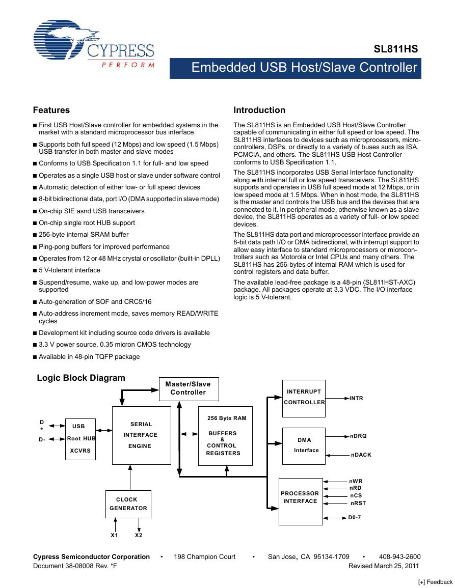
The SL811HS is an Embedded USB Host/Slave Controller
capable of communicating in either full speed or low speed. The
SL811HS interfaces to devices such as microprocessors, micro-
controllers, DSPs, or directly to a variety of buses such as ISA,
PCMCIA, and others. The SL811HS USB Host Controller
conforms to USB Specification 1.1.
The SL811HS incorporates USB Serial Interface functionality
along with internal full or low speed transceivers. The SL811HS
supports and operates in USB full speed mode at 12 Mbps, or in
low speed mode at 1.5 Mbps. When in host mode, the SL811HS
is the master and controls the USB bus and the devices that are
connected to it. In peripheral mode, otherwise known as a slave
device, the SL811HS operates as a variety of full- or low speed
devices.
The SL811HS data port and microprocessor interface provide an
8-bit data path I/O or DMA bidirectional, with interrupt support to
allow easy interface to standard microprocessors or microcon-
trollers such as Motorola or Intel CPUs and many others. The
SL811HS has 256-bytes of internal RAM which is used for
control registers and data buffer.
The available lead-free package is a 48-pin (SL811HST-AXC)
package. All packages operate at 3.3 VDC. The I/O interface
logic is 5 V-tolerant.
Master/Slave
Controller
256 Byte RAM
BUFFERS
&
CONTROL
REGISTERS
Logic Block Diagram
D
+
D-
USB
Root HUB
XCVRS
SERIAL
INTERFACE
ENGINE
CLOCK
GENERATOR
X1
X2
INTERRUPT
CONTROLLER
INTR
DMA
Interface
PROCESSOR
INTERFACE
nDRQ
nDACK
nWR
nRD
nCS
nRST
D0-7
Cypress Semiconductor Corporation
Document 38-08008 Rev. *F
•
198 Champion Court
•
San Jose, CA 95134-1709
•
408-943-2600
Revised March 25, 2011
[+] Feedback
�
SL811HS
Contents
Features .............................................................................1
Introduction .......................................................................1
Logic Block Diagram ........................................................1
Data Port, Microprocessor Interface ............................3
DMA Controller (slave mode only) ..............................3
Interrupt Controller ......................................................3
Buffer Memory .............................................................3
PLL Clock Generator ...................................................4
USB Transceiver .........................................................5
SL811HS Registers ...........................................................5
Physical Connections ....................................................20
48-Pin TQFP Physical Connections ..........................20
Electrical Specifications ................................................23
Absolute Maximum Ratings .......................................23
Recommended Operating Condition ........................23
External Clock Input Characteristics (X1) .................. 23
DC Characteristics .................................................... 24
USB Host Transceiver Characteristics ...................... 24
Bus Interface Timing Requirements .......................... 25
Ordering Information ...................................................... 29
Ordering Code Definitions ......................................... 29
Package Diagram ............................................................ 30
Acronyms ........................................................................ 30
Document Conventions ................................................. 30
Units of Measure ....................................................... 30
Document History Page ................................................ 31
Sales, Solutions, and Legal Information ...................... 32
Worldwide Sales and Design Support ....................... 32
Products .................................................................... 32
PSoC Solutions ......................................................... 32
Document 38-08008 Rev. *F
Page 2 of 32
[+] Feedback
�
SL811HS
Data Port, Microprocessor Interface
The SL811HS microprocessor interface provides an 8-bit
bidirectional data path along with appropriate control lines to
interface to external processors or controllers. Programmed I/O
or memory mapped I/O designs are supported through the 8-bit
interface, chip select, read and write input strobes, and a single
address line, A0.
Access to memory and control register space is a simple two
step process, requiring an address Write with A0 = ’0’, followed
by a register/memory Read or Write cycle with address line A0 =
’1’.
In addition, a DMA bidirectional interface in slave mode is
available with handshake signals such as nDRQ, nDACK, nWR,
nRD, nCS and INTRQ.
The SL811HS WRITE or READ operation terminates when
either nWR or nCS goes inactive. For devices interfacing to the
SL811HS that deactivate the Chip Select nCS before the Write
nWR, the data hold timing must be measured from the nCS and
is the same value as specified. Therefore, both Intel®- and
Motorola-type CPUs work easily with the SL811HS without any
external glue logic requirements.
DMA Controller (slave mode only)
In applications that require transfers of large amounts of data
such as scanner interfaces, the SL811HS provides a DMA inter-
face. This interface supports DMA READ or WRITE transfers to
the SL811HS internal RAM buffer, it is done through the micro-
processor data bus via two control lines (nDRQ - Data Request
and nDACK - Data Acknowledge), along with the nWR line and
controls the data flow into the SL811HS. The SL811HS has a
count register that allows selection of programmable block sizes
for DMA transfer. The control signals, both nDRQ and nDACK,
are designed for compatibility with standard DMA interfaces.
Interrupt Controller
The SL811HS interrupt controller provides a single output signal
(INTRQ) that is activated by a number of programmable events
that may occur as result of USB activity. Control and status
registers are provided to allow the user to select single or
multiple events, which generate an interrupt (assert INTRQ) and
let the user view interrupt status. The interrupts are cleared by
writing to the Interrupt Status Register.
Buffer Memory
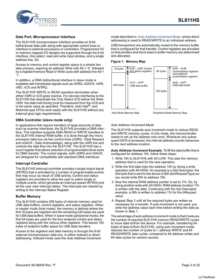
The SL811HS contains 256 bytes of internal memory used for
USB data buffers, control registers, and status registers. When
in master mode (host mode), the memory is defined where the
first 16 bytes are registers and the remaining 240 bytes are used
for USB data buffers. When in slave mode (peripheral mode), the
first 64 bytes are used for the four endpoint control and status
registers along with the various other registers. This leaves 192
bytes of endpoint buffer space for USB data transfers.
Access to the registers and data memory is through the 8-bit
external microprocessor data bus, in either indexed or direct
addressing. Indexed mode uses the Auto Address Increment
mode described in Auto Address Increment Mode, where direct
addressing is used to READ/WRITE to an individual address.
USB transactions are automatically routed to the memory buffer
that is configured for that transfer. Control registers are provided
so that pointers and block sizes in buffer memory are determined
and allocated.
Figure 1. Memory Map
16 bytes
0x00 – 0x0F Control
and status registers
64 bytes
240 bytes
0x10 – 0xFF
USB data buffer
192 bytes
0x00 – 0x39
Control/status registers
and endpoint
control/status registers
0x40 – 0xFF
USB data buffer
Host Mode Memory Map
Peripheral Mode Memory Map
Auto Address Increment Mode
The SL811HS supports auto increment mode to reduce READ
and WRITE memory cycles. In this mode, the microcontroller
needs to set up the address only once. Whenever any subse-
quent DATA is accessed, the internal address counter advances
to the next address location.
Auto Address Increment Example. To fill the data buffer that is
configured for address 10h, follow these steps:
1. Write 10h to SL811HS with A0 LOW. This sets the memory
address that is used for the next operation.
2. Write the first data byte into address 10h by doing a write
operation with A0 HIGH. An example is a Get Descriptor; the
first byte that is sent to the device is 80h (bmRequestType) so
you would write 80h to address 10h.
3. Now the internal RAM address pointer is set to 11h. So, by
doing another write with A0 HIGH, RAM address location 11h
is written with the data. Continuing with the Get Descriptor
example, a 06h is written to address 11h for the bRequest
value.
4. Repeat Step 3 until all the required bytes are written as
necessary for a transfer. If auto-increment is not used, you
write the address value each time before writing the data as
shown in Step 1.
The advantage of auto address increment mode is that it reduces
the number of required SL811HS memory READ/WRITE cycles
to move data to/from the device. For example, transferring 64
bytes of data to/from SL811HS, using auto increment mode,
reduces the number of cycles to 1 address WRITE and 64
READ/WRITE data cycles, compared to 64 address writes and
64 data cycles for random access.
Document 38-08008 Rev. *F
Page 3 of 32
[+] Feedback
�
SL811HS
PLL Clock Generator
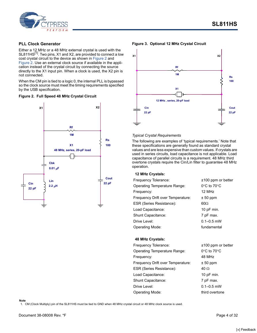
Either a 12 MHz or a 48 MHz external crystal is used with the
SL811HS[1]. Two pins, X1 and X2, are provided to connect a low
cost crystal circuit to the device as shown in Figure 2 and
Figure 2. Use an external clock source if available in the appli-
cation instead of the crystal circuit by connecting the source
directly to the X1 input pin. When a clock is used, the X2 pin is
not connected.
When the CM pin is tied to a logic 0, the internal PLL is bypassed
so the clock source must meet the timing requirements specified
by the USB specification.
Figure 2. Full Speed 48 MHz Crystal Circuit
X1
X2
Figure 3. Optional 12 MHz Crystal Circuit
X1
X2
Rf
1M
X1
12 MHz , series, 20-pF load
Cin
22 pF
Rs
100
Cout
22 pF
Rf
1M
X1
48 MHz, series, 20-pF load
Cbk
0.01 μF
Lin
2.2 μH
Cin
22 pF
Rs
100
Cout
22 pF
Typical Crystal Requirements
The following are examples of ‘typical requirements.’ Note that
these specifications are generally found as standard crystal
values and are less expensive than custom values. If crystals are
used in series circuits, load capacitance is not applicable. Load
capacitance of parallel circuits is a requirement. 48 MHz third
overtone crystals require the Cin/Lin filter to guarantee 48 MHz
operation.
12 MHz Crystals:
Frequency Tolerance:
Operating Temperature Range:
Frequency:
Frequency Drift over Temperature:
ESR (Series Resistance):
Load Capacitance:
Shunt Capacitance:
Drive Level:
Operating Mode:
48 MHz Crystals:
Frequency Tolerance:
Operating Temperature Range:
Frequency:
Frequency Drift over Temperature:
ESR (Series Resistance):
Load Capacitance:
Shunt Capacitance:
Drive Level:
Operating Mode:
±100 ppm or better
0°C to 70°C
12 MHz
± 50 ppm
60Ω
10 pF min.
7 pF max.
0.1–0.5 mW
fundamental
±100 ppm or better
0°C to 70°C
48 MHz
± 50 ppm
40 Ω
10 pF min.
7 pF max.
0.1–0.5 mW
third overtone
Note
1. CM (Clock Multiply) pin of the SL811HS must be tied to GND when 48 MHz crystal circuit or 48 MHz clock source is used.
Document 38-08008 Rev. *F
Page 4 of 32
[+] Feedback
�
SL811HS
USB Transceiver
The SL811HS has a built in transceiver that meets USB Specifi-
cation 1.1. The transceiver is capable of transmitting and
receiving serial data at USB full speed (12 Mbits) and low speed
(1.5 Mbits). The driver portion of the transceiver is differential
while the receiver section is comprised of a differential receiver
and two single-ended receivers. Internally, the transceiver inter-
faces to the Serial Interface Engine (SIE) logic. Externally, the
transceiver connects to the physical layer of the USB.
SL811HS Registers
Operation and control of the SL811HS is managed through
internal registers. When operating in Master/Host mode, the first
16 address locations are defined as register space. In
Slave/Peripheral mode, the first 64 bytes are defined as register
space. The register definitions vary greatly between each mode
of operation and are defined separately in this document (section
“Table 1 shows the memory map and register mapping of the
SL811HS in master/host mode.” on page 5 describes Host
register definitions, while section “SL811HS Slave Mode
Registers” on page 14 describes Slave register definitions).
Access to the registers are through the microprocessor interface
similar to normal RAM accesses (see “Bus Interface Timing
Requirements” on page 25) and provide control and status infor-
mation for USB transactions.
Any write to control register 0FH enables the SL811HS full
features bit. This is an internal bit of the SL811HS that enables
additional features.
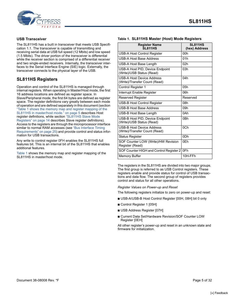
Table 1 shows the memory map and register mapping of the
SL811HS in master/host mode.
Table 1. SL811HS Master (Host) Mode Registers
SL811HS
Register Name
SL811HS
(hex) Address
04h
00h
01h
02h
03h
USB-A Host Control Register
USB-A Host Base Address
USB-A Host Base Length
USB-A Host PID, Device Endpoint
(Write)/USB Status (Read)
USB-A Host Device Address
(Write)/Transfer Count (Read)
Control Register 1
Interrupt Enable Register
Reserved Register
USB-B Host Control Register
USB-B Host Base Address
USB-B Host Base Length
USB-B Host PID, Device Endpoint
(Write)/USB Status (Read)
USB-B Host Device Address
(Write)/Transfer Count (Read)
Status Register
SOF Counter LOW (Write)/HW Revision
Register (Read)
SOF Counter HIGH and Control Register 2 0Fh
Memory Buffer
0Ch
0Dh
0Eh
05h
06h
Reserved
08h
09h
0Ah
0Bh
10H-FFh
The registers in the SL811HS are divided into two major groups.
The first group is referred to as USB Control registers. These
registers enable and provide status for control of USB transac-
tions and data flow. The second group of registers provides
control and status for all other operations.
Register Values on Power-up and Reset
The following registers initialize to zero on power-up and reset:
■ USB-A/USB-B Host Control Register [00H, 08H] bit 0 only
■ Control Register 1 [05H]
■ USB Address Register [07H]
■ Current Data Set/Hardware Revision/SOF Counter LOW
Register [0EH]
All other register’s power-up and reset in an unknown state and
firmware for initialization.
Document 38-08008 Rev. *F
Page 5 of 32
[+] Feedback
�
SL811HS
USB Control Registers
Communication and data flow on the USB bus uses the
SL811HS’ USB A-B Control registers. The SL811HS communi-
cates with any USB Device function and any specific endpoint
via the USB-A or USB-B register sets.
The USB A-B Host Control registers are used in an overlapped
configuration to manage traffic on the USB bus. The USB Host
Control register also provides a means to interrupt an external
CPU or microcontroller when one of the USB protocol transac-
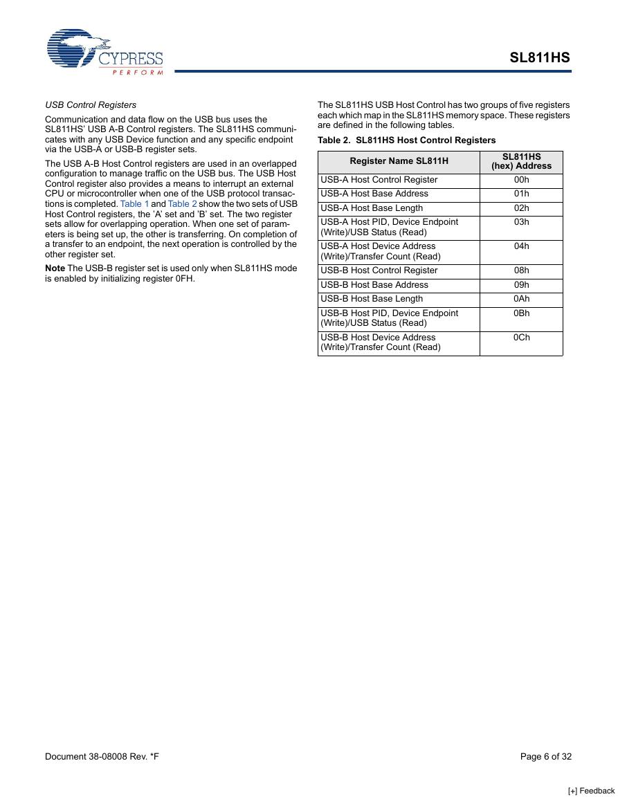
tions is completed. Table 1 and Table 2 show the two sets of USB
Host Control registers, the ’A’ set and ’B’ set. The two register
sets allow for overlapping operation. When one set of param-
eters is being set up, the other is transferring. On completion of
a transfer to an endpoint, the next operation is controlled by the
other register set.
Note The USB-B register set is used only when SL811HS mode
is enabled by initializing register 0FH.
The SL811HS USB Host Control has two groups of five registers
each which map in the SL811HS memory space. These registers
are defined in the following tables.
Table 2. SL811HS Host Control Registers
Register Name SL811H
USB-A Host Control Register
USB-A Host Base Address
USB-A Host Base Length
USB-A Host PID, Device Endpoint
(Write)/USB Status (Read)
USB-A Host Device Address
(Write)/Transfer Count (Read)
USB-B Host Control Register
USB-B Host Base Address
USB-B Host Base Length
USB-B Host PID, Device Endpoint
(Write)/USB Status (Read)
USB-B Host Device Address
(Write)/Transfer Count (Read)
SL811HS
(hex) Address
00h
01h
02h
03h
04h
08h
09h
0Ah
0Bh
0Ch
Document 38-08008 Rev. *F
Page 6 of 32
[+] Feedback
�
SL811HS
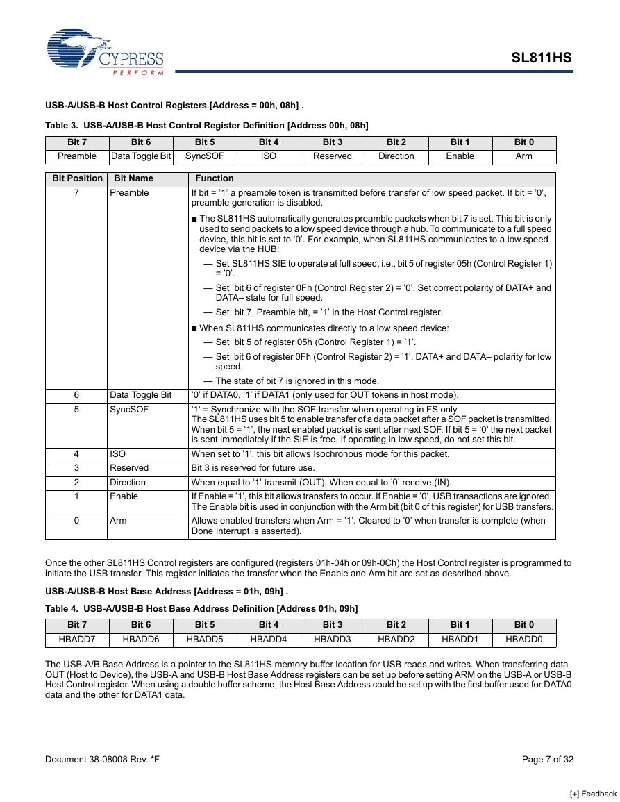
USB-A/USB-B Host Control Registers [Address = 00h, 08h] .
Table 3. USB-A/USB-B Host Control Register Definition [Address 00h, 08h]
Bit 7
Bit 6
Bit 5
Preamble
Data Toggle Bit
SyncSOF
Bit 4
ISO
Bit 3
Reserved
Bit 2
Direction
Bit 1
Enable
Bit 0
Arm
Bit Position Bit Name
Preamble
7
6
5
4
3
2
1
0
Data Toggle Bit
SyncSOF
ISO
Reserved
Direction
Enable
Arm
Function
If bit = ’1’ a preamble token is transmitted before transfer of low speed packet. If bit = ’0’,
preamble generation is disabled.
■ The SL811HS automatically generates preamble packets when bit 7 is set. This bit is only
used to send packets to a low speed device through a hub. To communicate to a full speed
device, this bit is set to ‘0’. For example, when SL811HS communicates to a low speed
device via the HUB:
— Set SL811HS SIE to operate at full speed, i.e., bit 5 of register 05h (Control Register 1)
= ’0’.
— Set bit 6 of register 0Fh (Control Register 2) = ’0’. Set correct polarity of DATA+ and
DATA– state for full speed.
— Set bit 7, Preamble bit, = ’1’ in the Host Control register.
■ When SL811HS communicates directly to a low speed device:
— Set bit 5 of register 05h (Control Register 1) = ’1’.
— Set bit 6 of register 0Fh (Control Register 2) = ’1’, DATA+ and DATA– polarity for low
speed.
— The state of bit 7 is ignored in this mode.
’0’ if DATA0, ’1’ if DATA1 (only used for OUT tokens in host mode).
’1’ = Synchronize with the SOF transfer when operating in FS only.
The SL811HS uses bit 5 to enable transfer of a data packet after a SOF packet is transmitted.
When bit 5 = ‘1’, the next enabled packet is sent after next SOF. If bit 5 = ‘0’ the next packet
is sent immediately if the SIE is free. If operating in low speed, do not set this bit.
When set to ’1’, this bit allows Isochronous mode for this packet.
Bit 3 is reserved for future use.
When equal to ’1’ transmit (OUT). When equal to ’0’ receive (IN).
If Enable = ’1’, this bit allows transfers to occur. If Enable = ’0’, USB transactions are ignored.
The Enable bit is used in conjunction with the Arm bit (bit 0 of this register) for USB transfers.
Allows enabled transfers when Arm = ’1’. Cleared to ’0’ when transfer is complete (when
Done Interrupt is asserted).
Once the other SL811HS Control registers are configured (registers 01h-04h or 09h-0Ch) the Host Control register is programmed to
initiate the USB transfer. This register initiates the transfer when the Enable and Arm bit are set as described above.
USB-A/USB-B Host Base Address [Address = 01h, 09h] .
Table 4. USB-A/USB-B Host Base Address Definition [Address 01h, 09h]
Bit 7
HBADD7
Bit 6
HBADD6
Bit 5
HBADD5
Bit 4
HBADD4
Bit 3
HBADD3
Bit 2
HBADD2
Bit 1
HBADD1
Bit 0
HBADD0
The USB-A/B Base Address is a pointer to the SL811HS memory buffer location for USB reads and writes. When transferring data
OUT (Host to Device), the USB-A and USB-B Host Base Address registers can be set up before setting ARM on the USB-A or USB-B
Host Control register. When using a double buffer scheme, the Host Base Address could be set up with the first buffer used for DATA0
data and the other for DATA1 data.
Document 38-08008 Rev. *F
Page 7 of 32
[+] Feedback
�
SL811HS
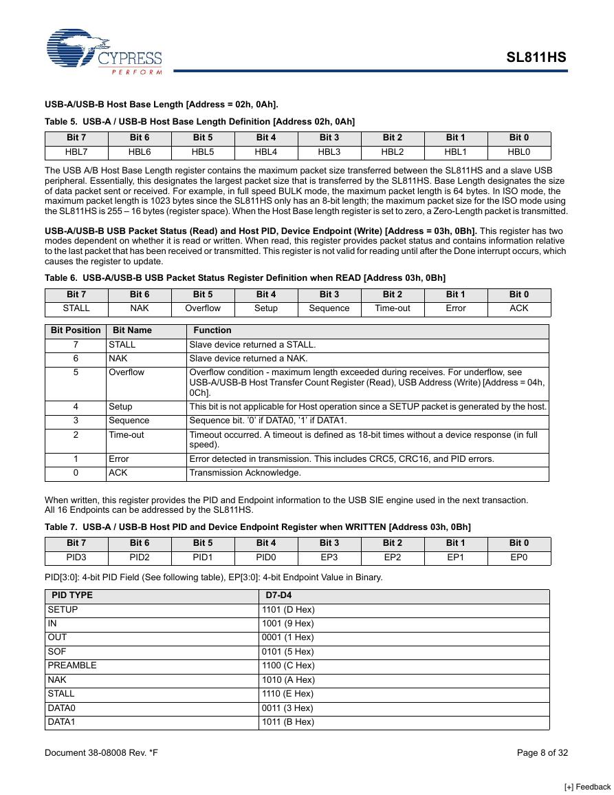
USB-A/USB-B Host Base Length [Address = 02h, 0Ah].
Table 5. USB-A / USB-B Host Base Length Definition [Address 02h, 0Ah]
Bit 7
HBL7
Bit 6
HBL6
Bit 5
HBL5
Bit 4
HBL4
Bit 3
HBL3
Bit 2
HBL2
Bit 1
HBL1
Bit 0
HBL0
The USB A/B Host Base Length register contains the maximum packet size transferred between the SL811HS and a slave USB
peripheral. Essentially, this designates the largest packet size that is transferred by the SL811HS. Base Length designates the size
of data packet sent or received. For example, in full speed BULK mode, the maximum packet length is 64 bytes. In ISO mode, the
maximum packet length is 1023 bytes since the SL811HS only has an 8-bit length; the maximum packet size for the ISO mode using
the SL811HS is 255 – 16 bytes (register space). When the Host Base length register is set to zero, a Zero-Length packet is transmitted.
USB-A/USB-B USB Packet Status (Read) and Host PID, Device Endpoint (Write) [Address = 03h, 0Bh]. This register has two
modes dependent on whether it is read or written. When read, this register provides packet status and contains information relative
to the last packet that has been received or transmitted. This register is not valid for reading until after the Done interrupt occurs, which
causes the register to update.
Table 6. USB-A/USB-B USB Packet Status Register Definition when READ [Address 03h, 0Bh]
Bit 7
STALL
Bit 6
NAK
Bit 5
Overflow
Bit 4
Setup
Bit 3
Sequence
Bit 2
Time-out
Bit 1
Error
Bit 0
ACK
Bit Position Bit Name
7
6
5
4
3
2
1
0
STALL
NAK
Overflow
Setup
Sequence
Time-out
Error
ACK
Function
Slave device returned a STALL.
Slave device returned a NAK.
Overflow condition - maximum length exceeded during receives. For underflow, see
USB-A/USB-B Host Transfer Count Register (Read), USB Address (Write) [Address = 04h,
0Ch].
This bit is not applicable for Host operation since a SETUP packet is generated by the host.
Sequence bit. ’0’ if DATA0, ’1’ if DATA1.
Timeout occurred. A timeout is defined as 18-bit times without a device response (in full
speed).
Error detected in transmission. This includes CRC5, CRC16, and PID errors.
Transmission Acknowledge.
When written, this register provides the PID and Endpoint information to the USB SIE engine used in the next transaction.
All 16 Endpoints can be addressed by the SL811HS.
Table 7. USB-A / USB-B Host PID and Device Endpoint Register when WRITTEN [Address 03h, 0Bh]
Bit 1
EP1
Bit 4
PID0
Bit 5
PID1
Bit 7
PID3
Bit 6
PID2
Bit 3
EP3
Bit 2
EP2
Bit 0
EP0
PID[3:0]: 4-bit PID Field (See following table), EP[3:0]: 4-bit Endpoint Value in Binary.
PID TYPE
SETUP
IN
OUT
SOF
PREAMBLE
NAK
STALL
DATA0
DATA1
Document 38-08008 Rev. *F
D7-D4
1101 (D Hex)
1001 (9 Hex)
0001 (1 Hex)
0101 (5 Hex)
1100 (C Hex)
1010 (A Hex)
1110 (E Hex)
0011 (3 Hex)
1011 (B Hex)
Page 8 of 32
[+] Feedback
�


 V2版本原理图(Capacitive-Fingerprint-Reader-Schematic_V2).pdf
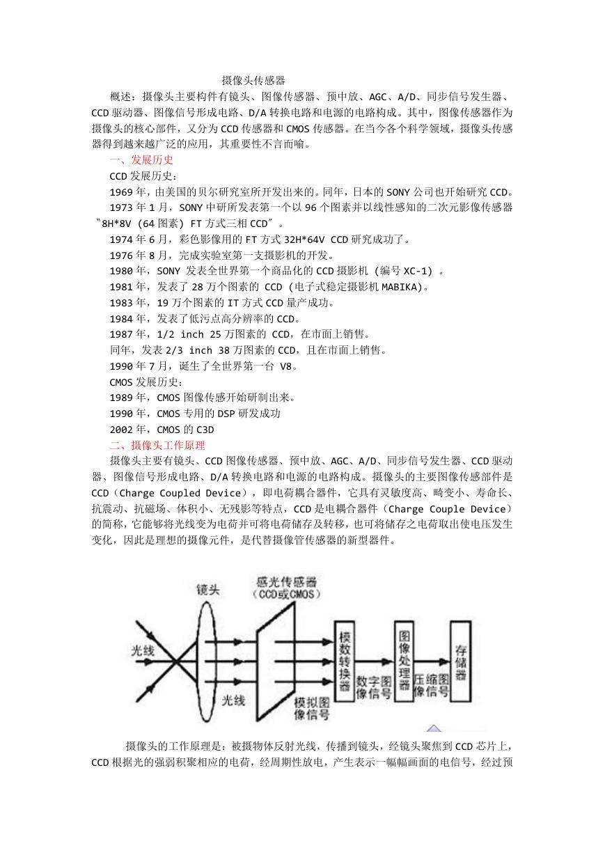 摄像头工作原理.doc
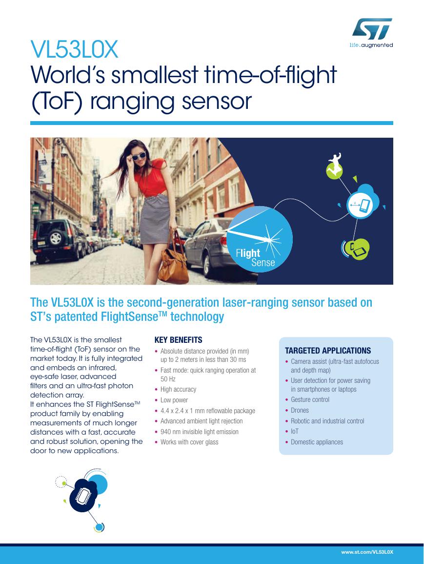 VL53L0X简要说明(En.FLVL53L00216).pdf
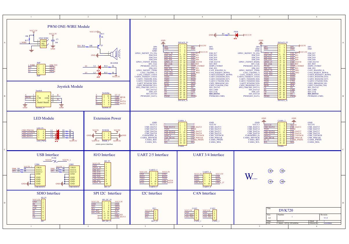 原理图(DVK720-Schematic).pdf
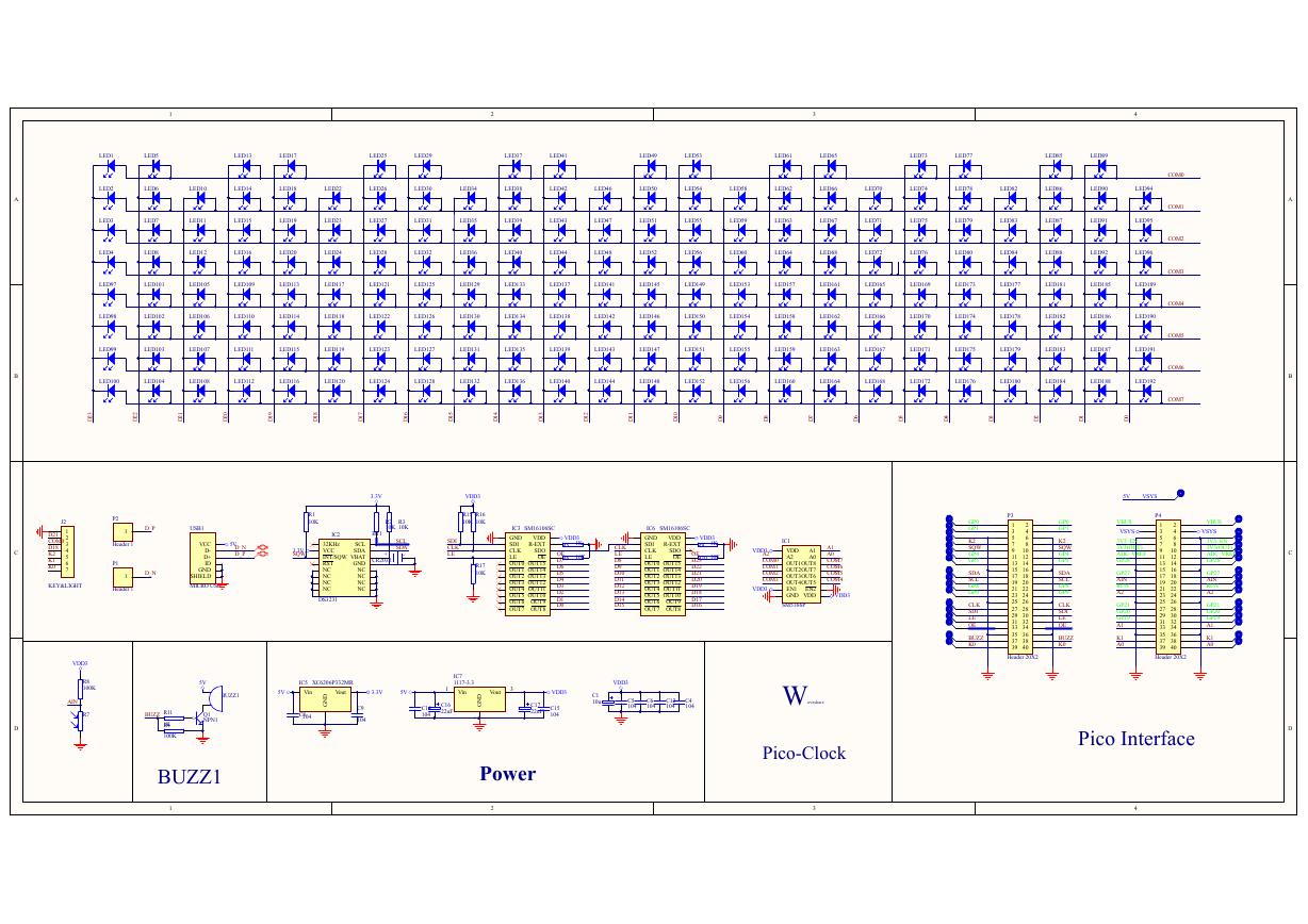 原理图(Pico-Clock-Green-Schdoc).pdf
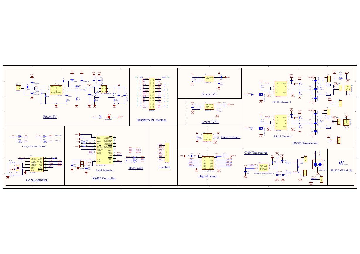 原理图(RS485-CAN-HAT-B-schematic).pdf
 File:SIM7500_SIM7600_SIM7800 Series_SSL_Application Note_V2.00.pdf
 ADS1263(Ads1262).pdf
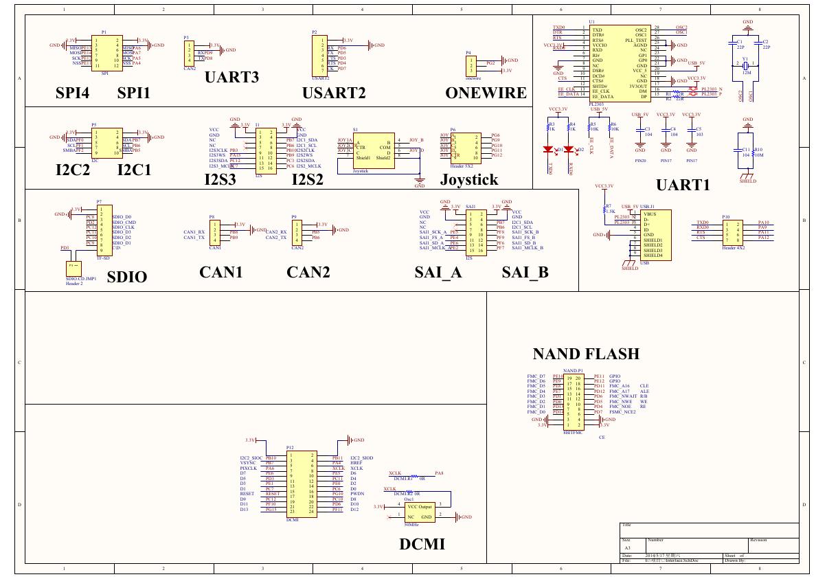 原理图(Open429Z-D-Schematic).pdf
 用户手册(Capacitive_Fingerprint_Reader_User_Manual_CN).pdf
 CY7C68013A(英文版)(CY7C68013A).pdf
 TechnicalReference_Dem.pdf