ADS1255
ADS1256
SBAS288D − JUNE 2003 − REVISED AUGUST 2004
Very Low Noise, 24ĆBit
AnalogĆtoĆDigital Converter
FEATURES
D 24 Bits, No Missing Codes
− All Data Rates and PGA Settings
D Up to 23 Bits Noise-Free Resolution
D ±0.0010% Nonlinearity (max)
D Data Output Rates to 30kSPS
D Fast Channel Cycling
− 18.6 Bits Noise-Free (21.3 Effective Bits)
at 1.45kHz
D One-Shot Conversions with Single-Cycle
Settling
D Flexible Input Multiplexer with Sensor Detect
− Four Differential Inputs (ADS1256 only)
− Eight Single-Ended Inputs (ADS1256 only)
D Chopper-Stabilized Input Buffer
D Low-Noise PGA: 27nV Input-Referred Noise
D Self and System Calibration for All PGA
Settings
D 5V Tolerant SPI-Compatible Serial Interface
D Analog Supply: 5V
D Digital Supply: 1.8V to 3.6V
D Power Dissipation
− As Low as 38mW in Normal Mode
− 0.4mW in Standby Mode
the
DESCRIPTION
The ADS1255 and ADS1256 are extremely low-noise,
24-bit analog-to-digital (A/D) converters. They provide
complete high-resolution measurement solutions for the
most demanding applications.
The converter is comprised of a 4th-order, delta-sigma
(∆Σ) modulator followed by a programmable digital filter. A
flexible
input multiplexer handles differential or
single-ended signals and includes circuitry to verify the
integrity of the external sensor connected to the inputs.
The selectable input buffer greatly increases the input
impedance and
low-noise programmable gain
amplifier (PGA) provides gains from 1 to 64 in binary steps.
The programmable filter allows the user to optimize
between a resolution of up to 23 bits noise-free and a data
rate of up to 30k samples per second (SPS). The
converters offer fast channel cycling for measuring
multiplexed inputs and can also perform one-shot
conversions that settle in just a single cycle.
Communication is handled over an SPI-compatible serial
interface that can operate with a 2-wire connection.
Onboard calibration supports both self and system
correction of offset and gain errors for all the PGA settings.
Bidirectional digital I/Os and a programmable clock output
driver are provided for general use. The ADS1255 is
packaged in an SSOP-20, and the ADS1256 in an
SSOP-28.
APPLICATIONS
D Weigh Scales
D Scientific Instrumentation
D Industrial Process Control
D Medical Equipment
D Test and Measurement
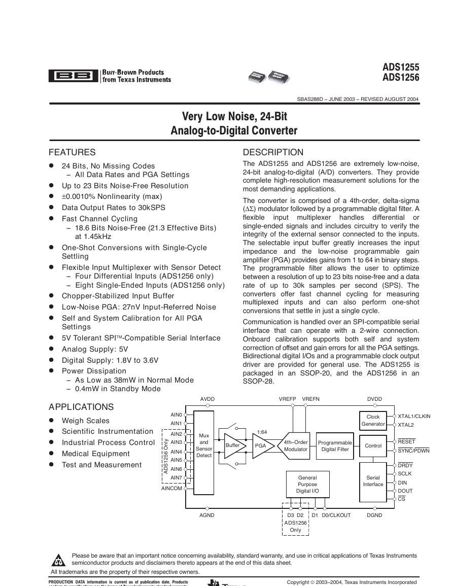
AIN0
AIN1
AIN2
AIN3
AIN4
AIN5
AIN6
AIN7
l
y
n
O
6
5
2
1
S
D
A
AINCOM
AVDD
VREFP VREFN
DVDD
1:64
PGA
Buffer
Mux
and
Sensor
Detect
Clock
Generator
XTAL1/CLKIN
XTAL2
4th−Order
Modulator
Programmable
Digital Filter
Control
RESET
SYNC/PDWN
General
Purpose
Digital I/O
Serial
Interface
DRDY
SCLK
DIN
DOUT
CS
AGND
D1 D0/CLKOUT
DGND
D3 D2
ADS1256
Only
Please be aware that an important notice concerning availability, standard warranty, and use in critical applications of Texas Instruments
semiconductor products and disclaimers thereto appears at the end of this data sheet.
All trademarks are the property of their respective owners.
PRODUCTION DATA
is current as of publication date. Products
conform to specifications per the terms of Texas Instruments standard warranty.
information
Copyright 2003−2004, Texas Instruments Incorporated
�
ADS1255
ADS1256
SBAS288D − JUNE 2003 − REVISED AUGUST 2004
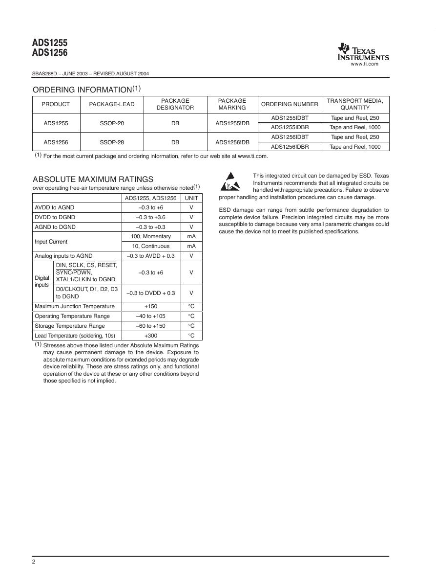
ORDERING INFORMATION(1)
PRODUCT
PACKAGE-LEAD
PACKAGE
DESIGNATOR
PACKAGE
MARKING
ORDERING NUMBER
ADS1255
ADS1255
SSOP-20
SSOP-20
ADS1256
ADS1256
SSOP-28
SSOP-28
DB
DB
DB
DB
ADS1255IDB
ADS1255IDB
ADS1256IDB
ADS1256IDB
(1) For the most current package and ordering information, refer to our web site at www.ti.com.
ADS1255IDBT
ADS1255IDBR
ADS1256IDBT
ADS1256IDBR
www.ti.com
TRANSPORT MEDIA,
QUANTITY
Tape and Reel, 250
Tape and Reel, 1000
Tape and Reel, 250
Tape and Reel, 1000
ABSOLUTE MAXIMUM RATINGS
over operating free-air temperature range unless otherwise noted(1)
UNIT
ADS1255, ADS1256
This integrated circuit can be damaged by ESD. Texas
Instruments recommends that all integrated circuits be
handled with appropriate precautions. Failure to observe
proper handling and installation procedures can cause damage.
ESD damage can range from subtle performance degradation to
complete device failure. Precision integrated circuits may be more
susceptible to damage because very small parametric changes could
cause the device not to meet its published specifications.
AVDD to AGND
DVDD to DGND
AGND to DGND
Input Current
Input Current
−0.3 to +6
−0.3 to +3.6
−0.3 to +0.3
100, Momentary
10, Continuous
Analog inputs to AGND
−0.3 to AVDD + 0.3
Digital
inputs
inputs
DIN, SCLK, CS, RESET,
SYNC/PDWN,
XTAL1/CLKIN to DGND
D0/CLKOUT, D1, D2, D3
to DGND
−0.3 to +6
−0.3 to DVDD + 0.3
V
V
V
mA
mA
V
V
V
+150
+300
−40 to +105
−60 to +150
°C
Maximum Junction Temperature
°C
Operating Temperature Range
°C
Storage Temperature Range
°C
Lead Temperature (soldering, 10s)
(1) Stresses above those listed under Absolute Maximum Ratings
may cause permanent damage to the device. Exposure to
absolute maximum conditions for extended periods may degrade
device reliability. These are stress ratings only, and functional
operation of the device at these or any other conditions beyond
those specified is not implied.
2
�
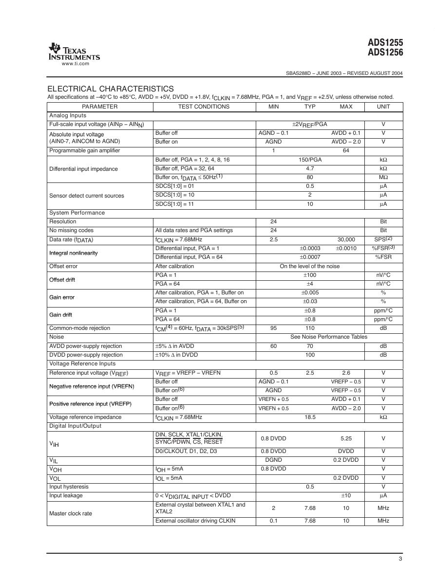
ADS1255ADS1256SBAS288D − JUNE 2003 − REVISED AUGUST 2004www.ti.com3ELECTRICAL CHARACTERISTICS All specifications at −40°C to +85°C, AVDD = +5V, DVDD = +1.8V, fCLKIN = 7.68MHz, PGA = 1, and VREF = +2.5V, unless otherwise noted.PARAMETERTEST CONDITIONSMINTYPMAXUNITAnalog InputsFull-scale input voltage (AINP − AINN)±2VREF/PGAVAbsolute input voltage(AIN0-7, AINCOM to AGND)Buffer offAGND − 0.1AVDD + 0.1VAbsolute input voltage(AIN0-7, AINCOM to AGND)Buffer onAGNDAVDD − 2.0VProgrammable gain amplifier164Buffer off, PGA = 1, 2, 4, 8, 16150/PGAkΩDifferential input impedanceBuffer off, PGA = 32, 644.7kΩDifferential input impedanceBuffer on, fDATA ≤ 50Hz(1)80MΩSDCS[1:0] = 010.5µASensor detect current sourcesSDCS[1:0] = 102µASensor detect current sourcesSDCS[1:0] = 1110µASystem PerformanceResolution24BitNo missing codesAll data rates and PGA settings24BitData rate (fDATA)fCLKIN = 7.68MHz2.530,000SPS(2)Integral nonlinearityDifferential input, PGA = 1±0.0003±0.0010%FSR(3)Integral nonlinearityDifferential input, PGA = 64±0.0007%FSROffset errorAfter calibrationOn the level of the noiseOffset driftPGA = 1±100nV/°COffset driftPGA = 64±4nV/°CGain errorAfter calibration, PGA = 1, Buffer on±0.005%Gain errorAfter calibration, PGA = 64, Buffer on±0.03%Gain driftPGA = 1±0.8ppm/°CGain driftPGA = 64±0.8ppm/°CCommon-mode rejectionfCM(4) = 60Hz, fDATA = 30kSPS(5)95110dBNoiseSee Noise Performance TablesAVDD power-supply rejection±5% ∆ in AVDD6070dBDVDD power-supply rejection±10% ∆ in DVDD100dBVoltage Reference InputsReference input voltage (VREF)VREF ≡ VREFP − VREFN0.52.52.6VNegative reference input (VREFN)Buffer offAGND − 0.1VREFP − 0.5VNegative reference input (VREFN)Buffer on(6)AGNDVREFP − 0.5VPositive reference input (VREFP)Buffer offVREFN + 0.5AVDD + 0.1VPositive reference input (VREFP)Buffer on(6)VREFN + 0.5AVDD − 2.0VVoltage reference impedancefCLKIN = 7.68MHz18.5kΩDigital Input/OutputVIHDIN, SCLK, XTAL1/CLKIN,SYNC/PDWN, CS, RESET0.8 DVDD5.25VVIHD0/CLKOUT, D1, D2, D30.8 DVDDDVDDVVILDGND0.2 DVDDVVOHIOH = 5mA0.8 DVDDVVOLIOL = 5mA0.2 DVDDVInput hysteresis0.5VInput leakage0 < VDIGITAL INPUT < DVDD±10µAMaster clock rateExternal crystal between XTAL1 andXTAL227.6810MHzMaster clock rateExternal oscillator driving CLKIN0.17.6810MHz�
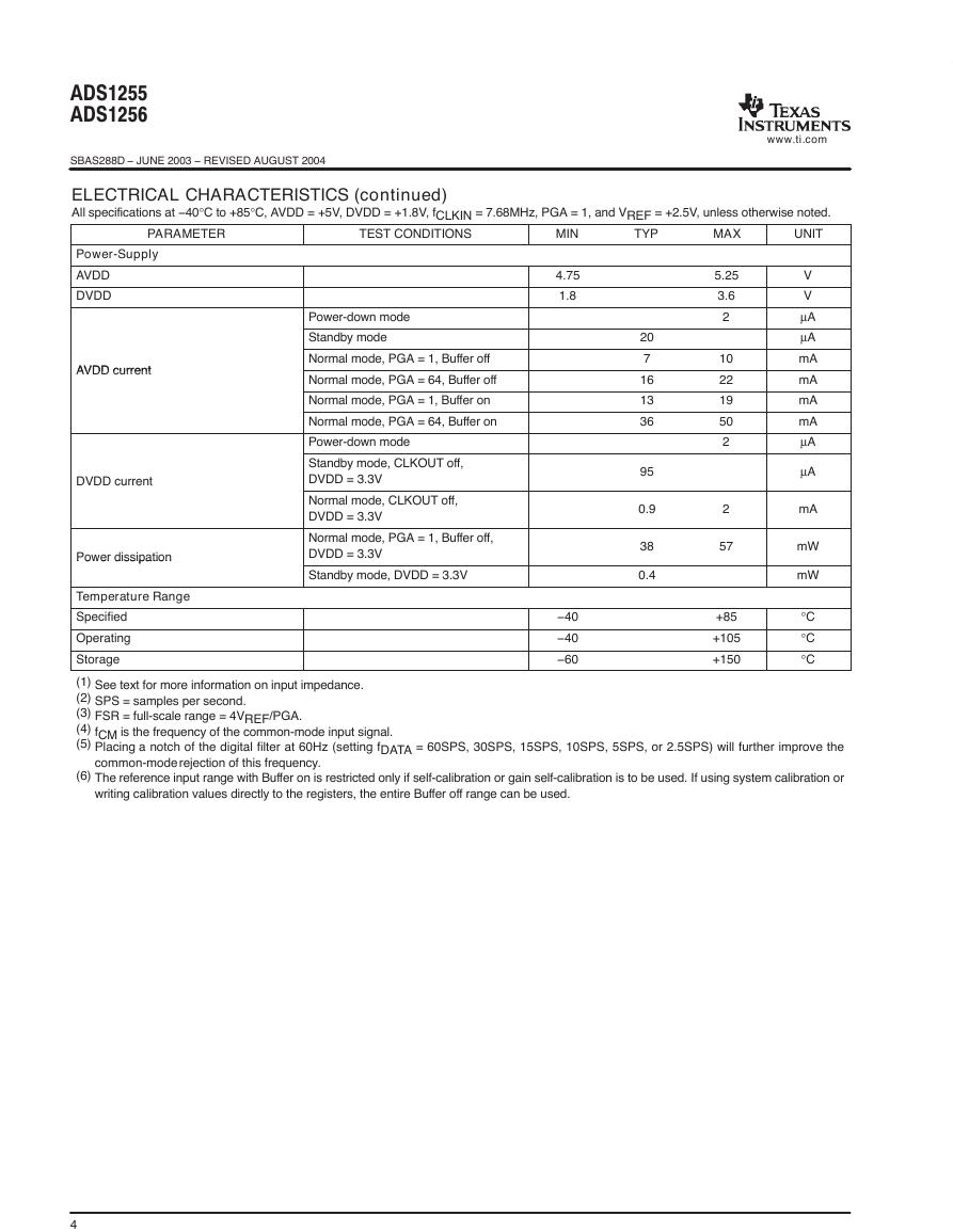
ADS1255ADS1256SBAS288D − JUNE 2003 − REVISED AUGUST 2004www.ti.com4ELECTRICAL CHARACTERISTICS (continued)All specifications at −40°C to +85°C, AVDD = +5V, DVDD = +1.8V, fCLKIN = 7.68MHz, PGA = 1, and VREF = +2.5V, unless otherwise noted.PARAMETERUNITMAXTYPMINTEST CONDITIONSPower-SupplyAVDD4.755.25VDVDD1.83.6VPower-down mode2µAStandby mode20µAAVDD currentNormal mode, PGA = 1, Buffer off710mAAVDD currentNormal mode, PGA = 64, Buffer off1622mANormal mode, PGA = 1, Buffer on1319mANormal mode, PGA = 64, Buffer on3650mAPower-down mode2µADVDD currentStandby mode, CLKOUT off,DVDD = 3.3V95µADVDD currentNormal mode, CLKOUT off,DVDD = 3.3V0.92mAPower dissipationNormal mode, PGA = 1, Buffer off,DVDD = 3.3V3857mWPower dissipationStandby mode, DVDD = 3.3V0.4mWTemperature RangeSpecified−40+85°COperating−40+105°CStorage−60+150°C(1)See text for more information on input impedance.(2)SPS = samples per second.(3)FSR = full-scale range = 4VREF/PGA.(4)fCM is the frequency of the common-mode input signal.(5)Placing a notch of the digital filter at 60Hz (setting fDATA = 60SPS, 30SPS, 15SPS, 10SPS, 5SPS, or 2.5SPS) will further improve thecommon-mode rejection of this frequency.(6)The reference input range with Buffer on is restricted only if self-calibration or gain self-calibration is to be used. If using system calibration orwriting calibration values directly to the registers, the entire Buffer off range can be used.�
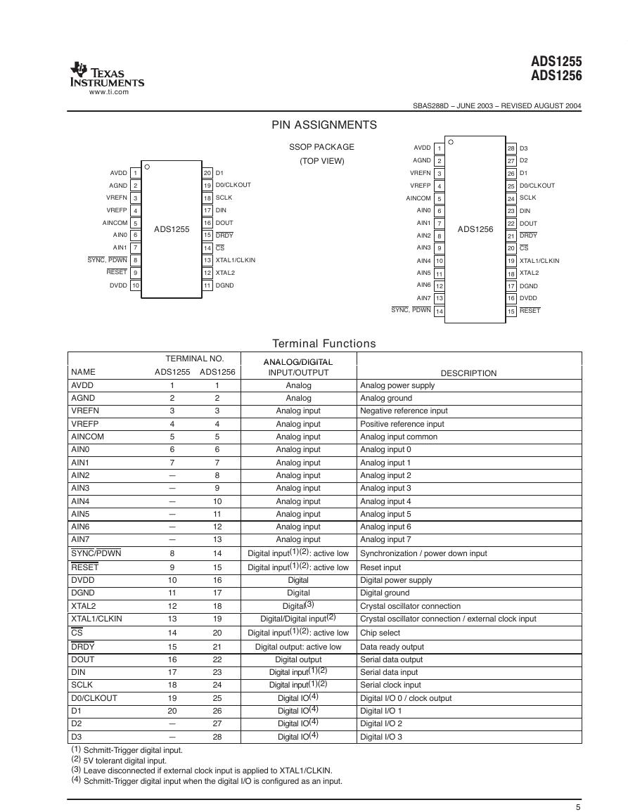
ADS1255ADS1256SBAS288D − JUNE 2003 − REVISED AUGUST 2004www.ti.com5PIN ASSIGNMENTSSSOP PACKAGE(TOP VIEW)ADS1255ADS1256AVDDAGNDVREFNVREFPAINCOMAIN0AIN1SYNC, PDWNRESETDVDDD1D0/CLKOUTSCLKDINDOUTDRDYCSXTAL1/CLKINXTAL2DGNDAVDDAGNDVREFNVREFPAINCOMAIN0AIN1SYNC, PDWNRESETDVDDAIN2AIN3AIN4AIN5AIN6AIN7D3D1D2D0/CLKOUTDINSCLKDOUTCSDRDYXTAL1/CLKINDGNDXTAL2123456789101112131415161718192098765432110131211142021222324252627281916171815Terminal FunctionsTERMINAL NO.ANALOG/DIGITALNAMEADS1255ADS1256ANALOG/DIGITALINPUT/OUTPUTDESCRIPTIONAVDD11AnalogAnalog power supplyAGND22AnalogAnalog groundVREFN33Analog inputNegative reference inputVREFP44Analog inputPositive reference inputAINCOM55Analog inputAnalog input commonAIN066Analog inputAnalog input 0AIN177Analog inputAnalog input 1AIN2—8Analog inputAnalog input 2AIN3—9Analog inputAnalog input 3AIN4—10Analog inputAnalog input 4AIN5—11Analog inputAnalog input 5AIN6—12Analog inputAnalog input 6AIN7—13Analog inputAnalog input 7SYNC/PDWN814Digital input(1)(2): active lowSynchronization / power down inputRESET915Digital input(1)(2): active lowReset inputDVDD1016DigitalDigital power supplyDGND1117DigitalDigital groundXTAL21218Digital(3)Crystal oscillator connectionXTAL1/CLKIN1319Digital/Digital input(2)Crystal oscillator connection / external clock inputCS1420Digital input(1)(2): active lowChip selectDRDY1521Digital output: active lowData ready outputDOUT1622Digital outputSerial data outputDIN1723Digital input(1)(2)Serial data inputSCLK1824Digital input(1)(2)Serial clock inputD0/CLKOUT1925Digital IO(4)Digital I/O 0 / clock outputD12026Digital IO(4)Digital I/O 1D2—27Digital IO(4)Digital I/O 2D3—28Digital IO(4)Digital I/O 3(1)Schmitt-Trigger digital input.(2)5V tolerant digital input.(3)Leave disconnected if external clock input is applied to XTAL1/CLKIN.(4)Schmitt-Trigger digital input when the digital I/O is configured as an input.�
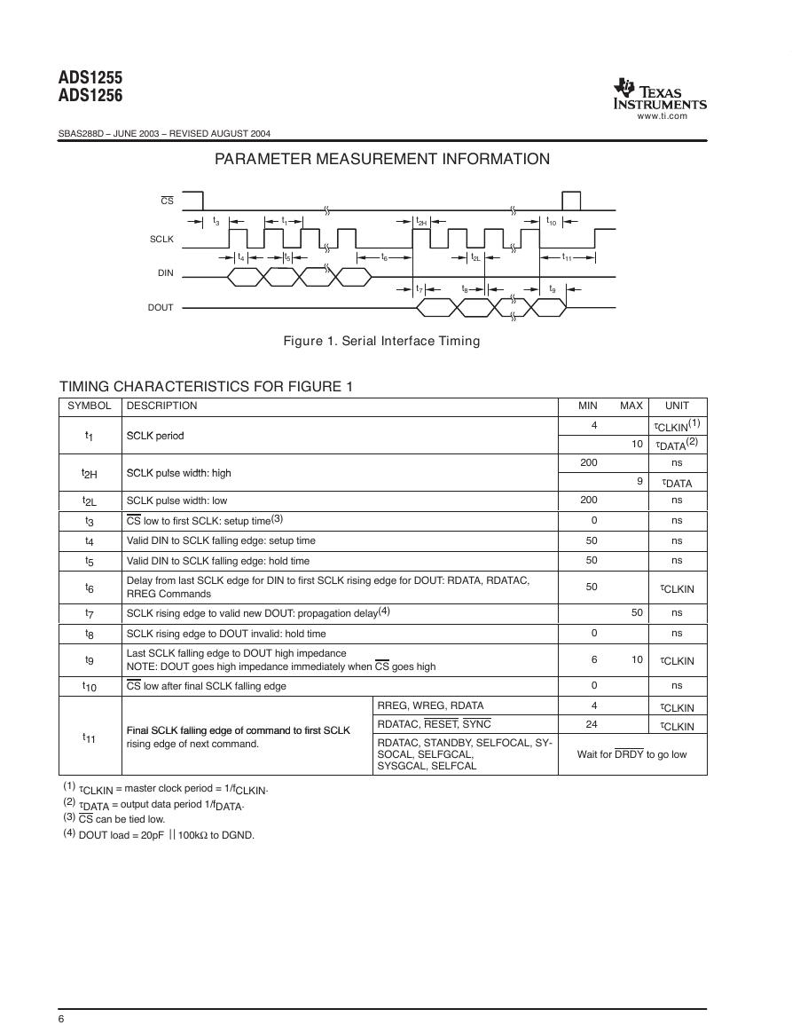
ADS1255ADS1256SBAS288D − JUNE 2003 − REVISED AUGUST 2004www.ti.com6PARAMETER MEASUREMENT INFORMATIONSCLKCSDINDOUTt1t3t2Ht4t5t2Lt6t9t8t7t11t10Figure 1. Serial Interface TimingTIMING CHARACTERISTICS FOR FIGURE 1 SYMBOLDESCRIPTIONMINMAXUNITt1SCLK period4τCLKIN(1)t1SCLK period10τDATA(2)t2HSCLK pulse width: high200nst2HSCLK pulse width: high9τDATAt2LSCLK pulse width: low200nst3CS low to first SCLK: setup time(3)0nst4Valid DIN to SCLK falling edge: setup time50nst5Valid DIN to SCLK falling edge: hold time50nst6Delay from last SCLK edge for DIN to first SCLK rising edge for DOUT: RDATA, RDATAC,RREG Commands50τCLKINt7SCLK rising edge to valid new DOUT: propagation delay(4)50nst8SCLK rising edge to DOUT invalid: hold time0nst9Last SCLK falling edge to DOUT high impedanceNOTE: DOUT goes high impedance immediately when CS goes high610τCLKINt10CS low after final SCLK falling edge0nsRREG, WREG, RDATA4τCLKINtFinal SCLK falling edge of command to first SCLKRDATAC, RESET, SYNC24τCLKINt11Final SCLK falling edge of command to first SCLKrising edge of next command.RDATAC, STANDBY, SELFOCAL, SY-SOCAL, SELFGCAL,SYSGCAL, SELFCALWait for DRDY to go low(1)τCLKIN = master clock period = 1/fCLKIN.(2)τDATA = output data period 1/fDATA.(3)CS can be tied low.(4)DOUT load = 20pF 100kΩ to DGND.�
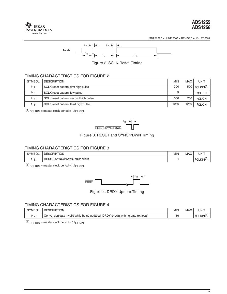
ADS1255ADS1256SBAS288D − JUNE 2003 − REVISED AUGUST 2004www.ti.com7SCLKt13t12t13t15t14Figure 2. SCLK Reset TimingTIMING CHARACTERISTICS FOR FIGURE 2 SYMBOLDESCRIPTIONMINMAXUNITt12SCLK reset pattern, first high pulse300500τCLKIN(1)t13SCLK reset pattern, low pulse5τCLKINt14SCLK reset pattern, second high pulse550750τCLKINt15SCLK reset pattern, third high pulse10501250τCLKIN(1)τCLKIN = master clock period = 1/fCLKIN.t16RESET,SYNC/PDWNFigure 3. RESET and SYNC/PDWN TimingTIMING CHARACTERISTICS FOR FIGURE 3 SYMBOLDESCRIPTIONMINMAXUNITt16RESET, SYNC/PDWN, pulse width4τCLKIN(1)(1)τCLKIN = master clock period = 1/fCLKIN.DRDYt17Figure 4. DRDY Update TimingTIMING CHARACTERISTICS FOR FIGURE 4 SYMBOLDESCRIPTIONMINMAXUNITt17Conversion data invalid while being updated (DRDY shown with no data retrieval)16τCLKIN(1)(1)τCLKIN = master clock period = 1/fCLKIN.�
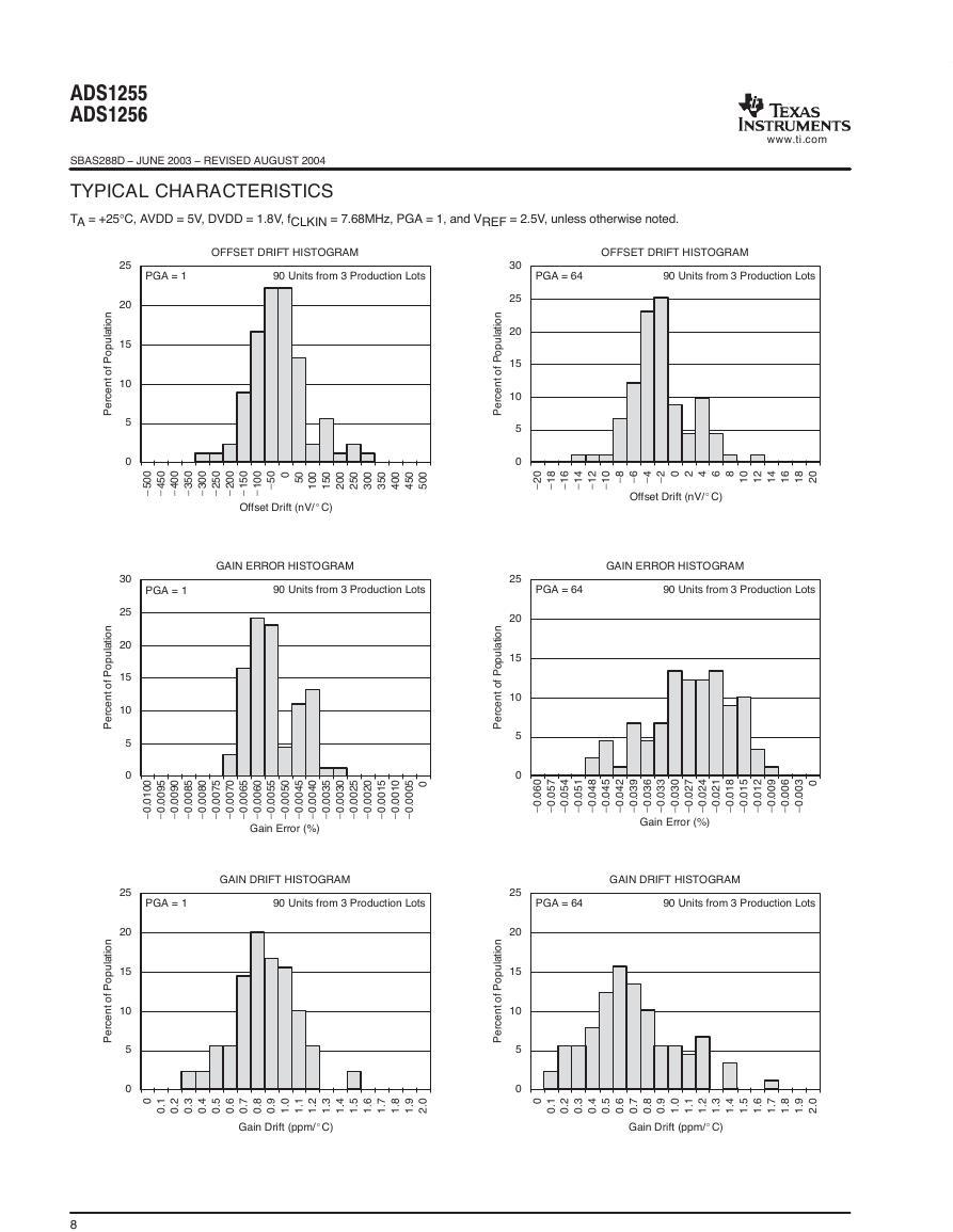
ADS1255ADS1256SBAS288D − JUNE 2003 − REVISED AUGUST 2004www.ti.com8TYPICAL CHARACTERISTICSTA = +25°C, AVDD = 5V, DVDD = 1.8V, fCLKIN = 7.68MHz, PGA = 1, and VREF = 2.5V, unless otherwise noted.OFFSETDRIFTHISTOGRAMPGA=190Unitsfrom3ProductionLotsOffsetDrift(nV/_C)2520151050PercentofPopulation−500−450−400−350−300−250−200−150−100−50050100150200250300350400450500OFFSETDRIFTHISTOGRAM90Unitsfrom3ProductionLotsOffsetDrift(nV/_C)302520151050PercentofPopulation−20−18−16−14−12−10−8−6−4−202468101214161820PGA=64GAINERRORHISTOGRAM90Unitsfrom3ProductionLotsGainError(%)302520151050PercentofPopulation−0.0100−0.0095−0.0090−0.0085−0.0080−0.0075−0.0070−0.0065−0.0060−0.0055−0.0050−0.0045−0.0040−0.0035−0.0030−0.0025−0.0020−0.0015−0.0010−0.00050PGA=1GAINERRORHISTOGRAM90Unitsfrom3ProductionLotsGainError(%)2520151050PercentofPopulation−0.060−0.057−0.054−0.051−0.048−0.045−0.042−0.039−0.036−0.033−0.030−0.027−0.024−0.021−0.018−0.015−0.012−0.009−0.006−0.0030PGA=64GAINDRIFTHISTOGRAM90Unitsfrom3ProductionLotsGainDrift(ppm/_C)2520151050PercentofPopulation00.10.20.30.40.50.60.70.80.91.01.11.21.31.41.51.61.71.81.92.0PGA=1GAINDRIFTHISTOGRAM90Unitsfrom3ProductionLotsGainDrift(ppm/_C)2520151050PercentofPopulation00.10.20.30.40.50.60.70.80.91.01.11.21.31.41.51.61.71.81.92.0PGA=64�


 V2版本原理图(Capacitive-Fingerprint-Reader-Schematic_V2).pdf
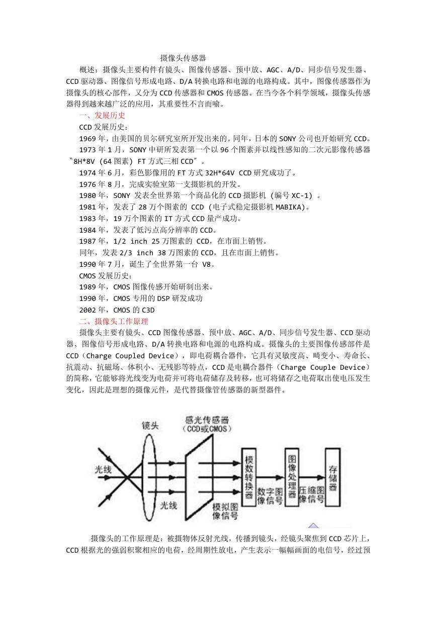 摄像头工作原理.doc
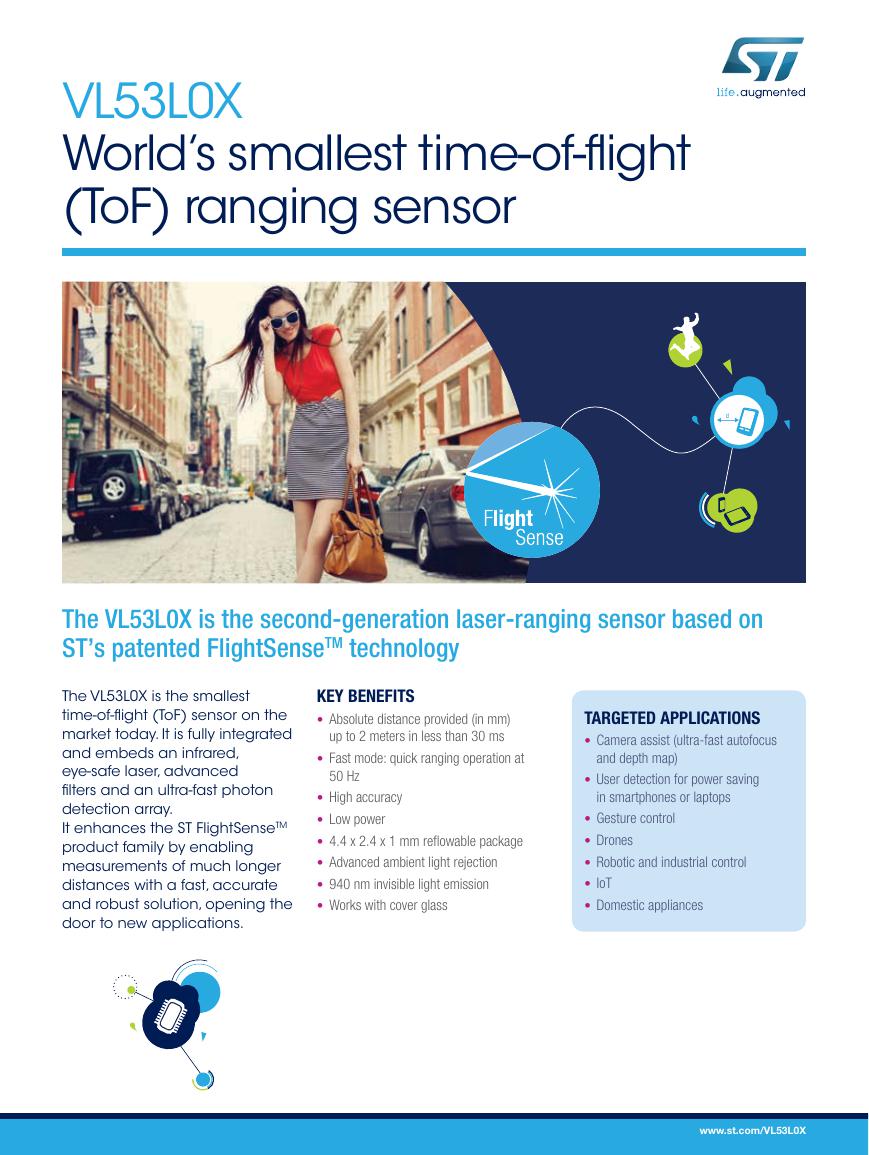 VL53L0X简要说明(En.FLVL53L00216).pdf
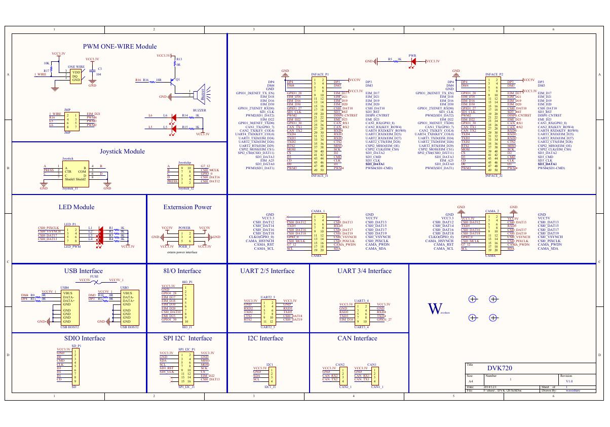 原理图(DVK720-Schematic).pdf
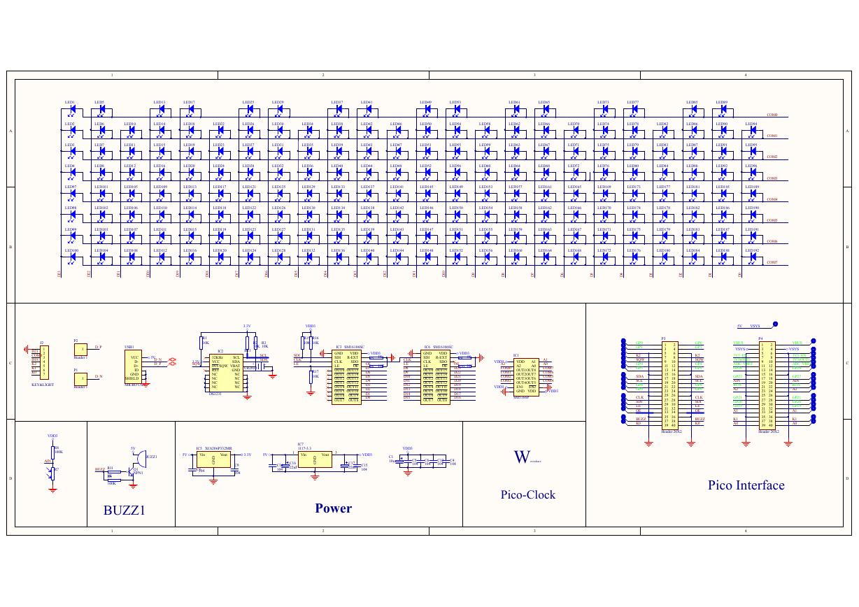 原理图(Pico-Clock-Green-Schdoc).pdf
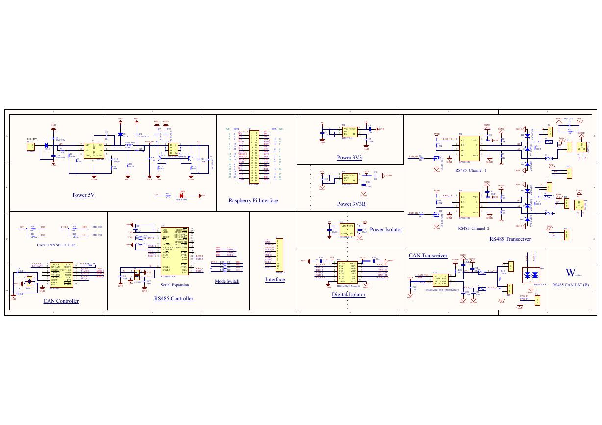 原理图(RS485-CAN-HAT-B-schematic).pdf
 File:SIM7500_SIM7600_SIM7800 Series_SSL_Application Note_V2.00.pdf
 ADS1263(Ads1262).pdf
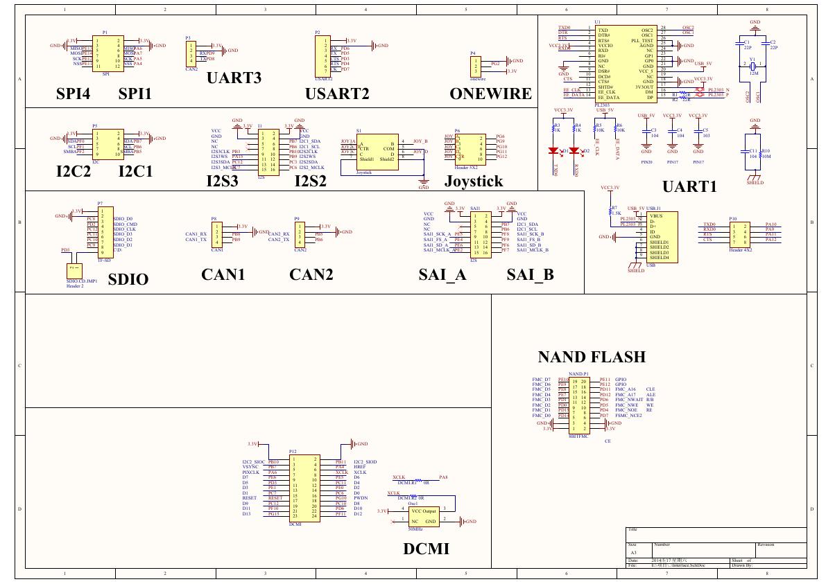 原理图(Open429Z-D-Schematic).pdf
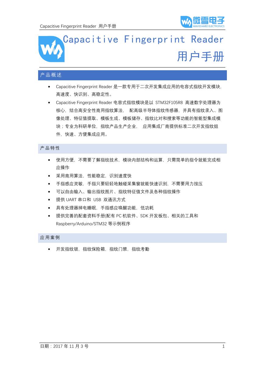 用户手册(Capacitive_Fingerprint_Reader_User_Manual_CN).pdf
 CY7C68013A(英文版)(CY7C68013A).pdf
 TechnicalReference_Dem.pdf