SC16IS752/SC16IS762
Dual UART with I2C-bus/SPI interface, 64 bytes of transmit
and receive FIFOs, IrDA SIR built-in support
Rev. 07 — 19 May 2008
Product data sheet
1. General description
The SC16IS752/SC16IS762 is an I2C-bus/SPI bus interface to a dual-channel high
performance UART offering data rates up to 5 Mbit/s, low operating and sleeping current;
it also provides the application with 8 additional programmable I/O pins. The device comes
in very small HVQFN32 and TSSOP28 packages, which makes it ideally suitable for
hand-held, battery-operated applications. This chip enables seamless protocol conversion
from I2C-bus/SPI to RS-232/RS-485 and is fully bidirectional.
The SC16IS762 differs from the SC16IS752 in that it supports SPI clock speeds up to
15 Mbit/s instead of the 4 Mbit/s supported by the SC16IS752, and in that it supports IrDA
SIR up to 1.152 Mbit/s. In all other aspects, the SC16IS762 is functionally and electrically
the same as the SC16IS752.
The SC16IS752/SC16IS762’s internal register set is backward compatible with the widely
used and widely popular 16C450. This allows the software to be easily written or ported
from another platform.
The SC16IS752/SC16IS762 also provides additional advanced features such as auto
hardware and software flow control, automatic RS-485 support and software reset. This
allows the software to reset the UART at any moment, independent of the hardware reset
signal.
2. Features
2.1 General features
n Dual full-duplex UART
n I2C-bus or SPI interface selectable
n 3.3 V or 2.5 V operation
n Industrial temperature range: - 40 C to +95 C
n 64 bytes FIFO (transmitter and receiver)
n Fully compatible with industrial standard 16C450 and equivalent
n Baud rates up to 5 Mbit/s in 16· clock mode
n Auto hardware flow control using RTS/CTS
n Auto software flow control with programmable Xon/Xoff characters
n Single or double Xon/Xoff characters
n Automatic RS-485 support (automatic slave address detection)
n Up to eight programmable I/O pins
n RS-485 driver direction control via RTS signal
�
NXP Semiconductors
SC16IS752/SC16IS762
Dual UART with I2C-bus/SPI interface, 64-byte FIFOs, IrDA SIR
n RS-485 driver direction control inversion
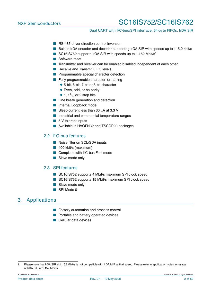
n Built-in IrDA encoder and decoder supporting IrDA SIR with speeds up to 115.2 kbit/s
n SC16IS762 supports IrDA SIR with speeds up to 1.152 Mbit/s1
n Software reset
n Transmitter and receiver can be enabled/disabled independent of each other
n Receive and Transmit FIFO levels
n Programmable special character detection
n Fully programmable character formatting
u 5-bit, 6-bit, 7-bit or 8-bit character
u Even, odd, or no parity
u 1, 11⁄2, or 2 stop bits
n Line break generation and detection
n Internal Loopback mode
n Sleep current less than 30 m A at 3.3 V
n Industrial and commercial temperature ranges
n 5 V tolerant inputs
n Available in HVQFN32 and TSSOP28 packages
2.2 I2C-bus features
n Noise filter on SCL/SDA inputs
n 400 kbit/s (maximum)
n Compliant with I2C-bus Fast mode
n Slave mode only
2.3 SPI features
n SC16IS752 supports 4 Mbit/s maximum SPI clock speed
n SC16IS762 supports 15 Mbit/s maximum SPI clock speed
n Slave mode only
n SPI Mode 0
3. Applications
n Factory automation and process control
n Portable and battery operated devices
n Cellular data devices
1.
Please note that IrDA SIR at 1.152 Mbit/s is not compatible with IrDA MIR at that speed. Please refer to application notes for usage
of IrDA SIR at 1.152 Mbit/s.
SC16IS752_SC16IS762_7
Product data sheet
Rev. 07 — 19 May 2008
© NXP B.V. 2008. All rights reserved.
2 of 59
�
NXP Semiconductors
SC16IS752/SC16IS762
Dual UART with I2C-bus/SPI interface, 64-byte FIFOs, IrDA SIR
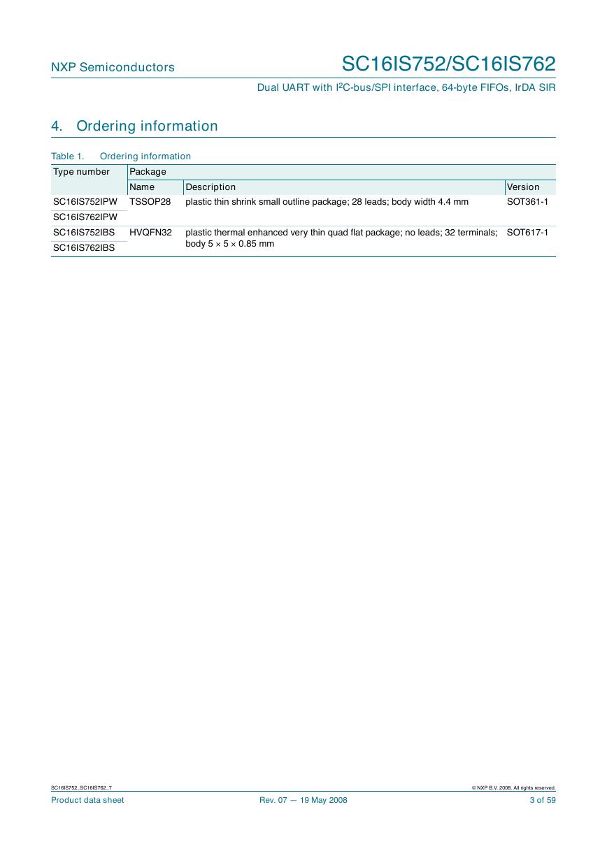
4. Ordering information
Table 1.
Type number
Ordering information
Package
Name
SC16IS752IPW TSSOP28
SC16IS762IPW
SC16IS752IBS
SC16IS762IBS
HVQFN32
Description
plastic thin shrink small outline package; 28 leads; body width 4.4 mm
Version
SOT361-1
plastic thermal enhanced very thin quad flat package; no leads; 32 terminals;
body 5 · 5 · 0.85 mm
SOT617-1
SC16IS752_SC16IS762_7
Product data sheet
Rev. 07 — 19 May 2008
© NXP B.V. 2008. All rights reserved.
3 of 59
�
NXP Semiconductors
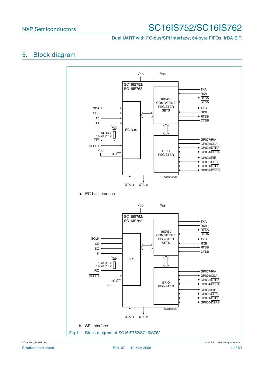
5. Block diagram
SC16IS752/SC16IS762
Dual UART with I2C-bus/SPI interface, 64-byte FIFOs, IrDA SIR
VDD
VSS
SC16IS752/
SC16IS762
16C450
COMPATIBLE
REGISTER
SETS
SDA
SCL
A0
A1
VDD
1 kW
1.5 kW
(3.3 V)
(2.5 V)
I2C-BUS
IRQ
RESET
VDD
I2C/SPI
GPIO
REGISTER
a.
I2C-bus interface
002aab207
XTAL1
XTAL2
VDD
VSS
SC16IS752/
SC16IS762
SCLK
CS
SO
SI
VDD
1 kW
1.5 kW
(3.3 V)
(2.5 V)
IRQ
RESET
I2C/SPI
SPI
16C450
COMPATIBLE
REGISTER
SETS
GPIO
REGISTER
002aab598
XTAL1
XTAL2
b. SPI interface
Fig 1. Block diagram of SC16IS752/SC16IS762
TXA
RXA
RTSA
CTSA
TXB
RXB
RTSB
CTSB
GPIO7/RIA
GPIO6/CDA
GPIO5/DTRA
GPIO4/DSRA
GPIO3/RIB
GPIO2/CDB
GPIO1/DTRB
GPIO0/DSRB
TXA
RXA
RTSA
CTSA
TXB
RXB
RTSB
CTSB
GPIO7/RIA
GPIO6/CDA
GPIO5/DTRA
GPIO4/DSRA
GPIO3/RIB
GPIO2/CDB
GPIO1/DTRB
GPIO0/DSRB
SC16IS752_SC16IS762_7
Product data sheet
Rev. 07 — 19 May 2008
© NXP B.V. 2008. All rights reserved.
4 of 59
�
NXP Semiconductors
SC16IS752/SC16IS762
Dual UART with I2C-bus/SPI interface, 64-byte FIFOs, IrDA SIR
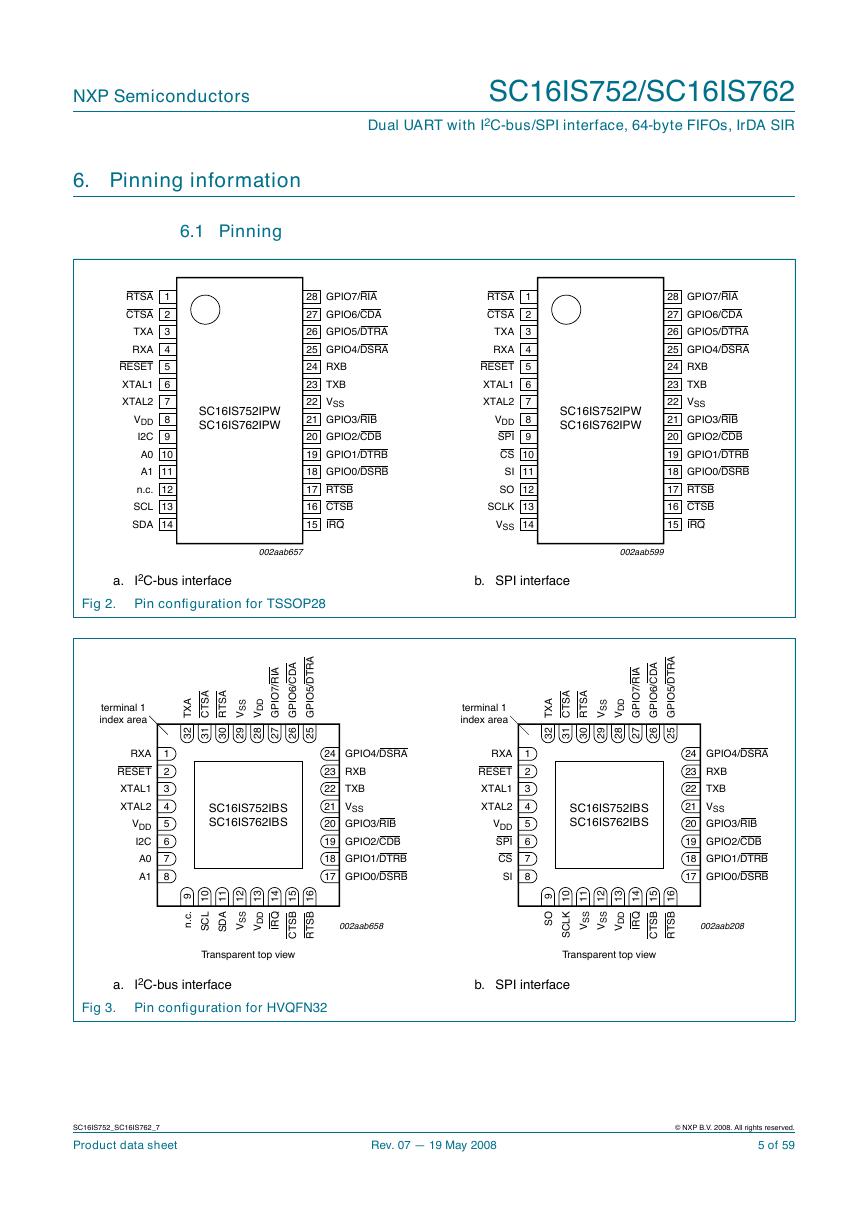
6. Pinning information
6.1 Pinning
RTSA
CTSA
TXA
RXA
RESET
XTAL1
XTAL2
VDD
I2C
A0
A1
n.c.
SCL
SDA
1
2
3
4
5
6
7
8
9
10
11
12
13
14
SC16IS752IPW
SC16IS762IPW
28
27
26
25
24
23
22
21
20
19
18
17
16
15
GPIO7/RIA
GPIO6/CDA
GPIO5/DTRA
GPIO4/DSRA
RXB
TXB
VSS
GPIO3/RIB
GPIO2/CDB
GPIO1/DTRB
GPIO0/DSRB
RTSB
CTSB
IRQ
RTSA
CTSA
TXA
RXA
RESET
XTAL1
XTAL2
VDD
SPI
CS
SI
SO
SCLK
VSS
1
2
3
4
5
6
7
8
9
10
11
12
13
14
SC16IS752IPW
SC16IS762IPW
28
27
26
25
24
23
22
21
20
19
18
17
16
15
GPIO7/RIA
GPIO6/CDA
GPIO5/DTRA
GPIO4/DSRA
RXB
TXB
VSS
GPIO3/RIB
GPIO2/CDB
GPIO1/DTRB
GPIO0/DSRB
RTSB
CTSB
IRQ
002aab657
002aab599
a.
Fig 2.
I2C-bus interface
Pin configuration for TSSOP28
b. SPI interface
terminal 1
index area
A
S
T
C
A
S
T
R
A
X
T
S
S
V
D
D
V
I
A
R
/
7
O
P
G
I
A
R
T
D
/
5
O
P
G
I
A
D
C
/
6
O
P
G
I
terminal 1
index area
A
S
T
C
A
S
T
R
A
X
T
S
S
V
D
D
V
A
R
T
D
/
5
O
P
G
I
A
D
C
/
6
O
P
G
I
I
A
R
/
7
O
P
G
I
2
3
1
3
0
3
9
2
8
2
7
2
6
2
5
2
2
3
1
3
0
3
9
2
8
2
7
2
6
2
5
2
RXA
RESET
XTAL1
XTAL2
VDD
I2C
A0
A1
1
2
3
4
5
6
7
8
24
23
22
21
20
19
18
17
GPIO4/DSRA
RXB
TXB
VSS
GPIO3/RIB
GPIO2/CDB
GPIO1/DTRB
GPIO0/DSRB
002aab658
SC16IS752IBS
SC16IS762IBS
9
0
1
1
1
2
1
3
1
4
1
5
1
6
1
.
c
.
n
L
C
S
A
D
S
S
S
V
D
D
V
Q
R
I
B
S
T
C
B
S
T
R
Transparent top view
RXA
RESET
XTAL1
XTAL2
VDD
SPI
CS
SI
1
2
3
4
5
6
7
8
24
23
22
21
20
19
18
17
GPIO4/DSRA
RXB
TXB
VSS
GPIO3/RIB
GPIO2/CDB
GPIO1/DTRB
GPIO0/DSRB
002aab208
SC16IS752IBS
SC16IS762IBS
9
0
1
1
1
2
1
3
1
4
1
5
1
6
1
O
S
K
L
C
S
S
S
V
S
S
V
D
D
V
Q
R
I
B
S
T
C
B
S
T
R
Transparent top view
a.
Fig 3.
I2C-bus interface
Pin configuration for HVQFN32
b. SPI interface
SC16IS752_SC16IS762_7
Product data sheet
Rev. 07 — 19 May 2008
© NXP B.V. 2008. All rights reserved.
5 of 59
�
NXP Semiconductors
SC16IS752/SC16IS762
Dual UART with I2C-bus/SPI interface, 64-byte FIFOs, IrDA SIR
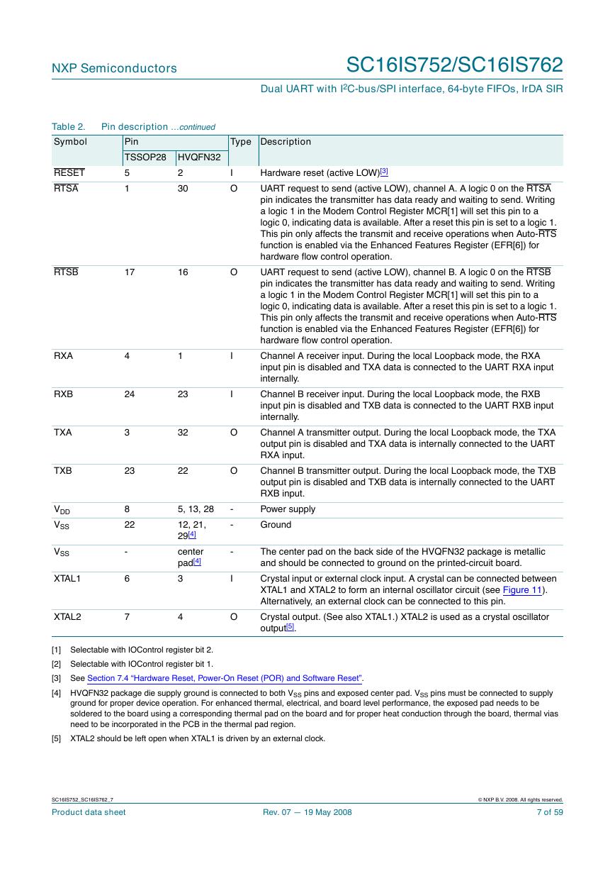
6.2 Pin description
Table 2.
Symbol
CS/A0
Pin description
Pin
TSSOP28 HVQFN32
10
7
CTSA
2
31
CTSB
16
15
I2C/SPI
IRQ
9
15
SI/A1
11
SO
SCL/SCLK
SDA
GPIO0/DSRB
GPIO1/DTRB
GPIO2/CDB
GPIO3/RIB
GPIO4/DSRA
GPIO5/DTRA
GPIO6/CDA
GPIO7/RIA
12
13
14
18
19
20
21
25
26
27
28
SC16IS752_SC16IS762_7
Product data sheet
6
14
8
9
10
11
17
18
19
20
24
25
26
27
Type Description
I
I
I
I
O
I
O
I
I/O
I/O
I/O
I/O
I/O
I/O
I/O
I/O
I/O
SPI chip select or I2C-bus device address select A0. If SPI configuration
is selected by I2C/SPI pin, this pin is the SPI chip select pin
(Schmitt-trigger active LOW). If I2C-bus configuration is selected by
I2C/SPI pin, this pin along with A1 pin allows user to change the device’s
base address.
To select the device address, please refer to Table 32.
UART clear to send (active LOW), channel A. A logic 0 (LOW) on the
CTSA pin indicates the modem or data set is ready to accept transmit
data from the SC16IS752/SC16IS762. Status can be tested by reading
MSR[4]. This pin only affects the transmit and receive operations when
Auto-CTS function is enabled via the Enhanced Features Register
EFR[7] for hardware flow control operation.
UART clear to send (active LOW), channel B. A logic 0 on the CTSB pin
indicates the modem or data set is ready to accept transmit data from the
SC16IS752/SC16IS762. Status can be tested by reading MSR[4]. This
pin only affects the transmit and receive operations when Auto-CTS
function is enabled via the Enhanced Features Register EFR[7] for
hardware flow control operation.
I2C-bus or SPI interface select. I2C-bus interface is selected if this pin is
at logic HIGH. SPI interface is selected if this pin is at logic LOW.
Interrupt (open-drain, active LOW). Interrupt is enabled when interrupt
sources are enabled in the Interrupt Enable Register (IER). Interrupt
conditions include: change of state of the input pins, receiver errors,
available receiver buffer data, available transmit buffer space, or when a
modem status flag is detected. An external resistor (1 kW
1.5 kW
SPI data input pin or I2C-bus device address select A1. If SPI
configuration is selected by I2C/SPI pin, this is the SPI data input pin. If
I2C-bus configuration is selected by I2C/SPI pin, this pin along with the
A0 pin allows user to change the slave base address. To select the
device address, please refer to Table 32.
SPI data output pin. If SPI configuration is selected by I2C/SPI pin, this is
a 3-stateable output pin. If I2C-bus configuration is selected by the
I2C/SPI pin, this pin is undefined and must be left as not connected.
I2C-bus or SPI input clock.
I2C-bus data input/output, open-drain if I2C-bus configuration is selected
by I2C/SPI pin. If SPI configuration is selected, this is not used and must
be connected to VSS.
Programmable I/O pin or modem DSRB[1]
Programmable I/O pin or modem DTRB[1]
Programmable I/O pin or modem CDB[1]
Programmable I/O pin or modem RIB[1]
Programmable I/O pin or modem DSRA[2]
Programmable I/O pin or modem DTRA[2]
Programmable I/O pin or modem CDA[2]
Programmable I/O pin or modem RIA[2]
for 2.5 V) must be connected between this pin and VDD.
for 3.3 V,
Rev. 07 — 19 May 2008
© NXP B.V. 2008. All rights reserved.
6 of 59
�
NXP Semiconductors
SC16IS752/SC16IS762
Dual UART with I2C-bus/SPI interface, 64-byte FIFOs, IrDA SIR
Table 2.
Symbol
RESET
RTSA
Pin description …continued
Pin
TSSOP28 HVQFN32
5
1
2
30
I
O
RTSB
17
16
O
RXA
RXB
TXA
TXB
VDD
VSS
VSS
XTAL1
XTAL2
4
24
3
23
8
22
-
6
7
1
23
32
22
5, 13, 28
12, 21,
29[4]
center
pad[4]
3
I
I
O
O
-
-
-
I
4
O
Type Description
Hardware reset (active LOW)[3]
UART request to send (active LOW), channel A. A logic 0 on the RTSA
pin indicates the transmitter has data ready and waiting to send. Writing
a logic 1 in the Modem Control Register MCR[1] will set this pin to a
logic 0, indicating data is available. After a reset this pin is set to a logic 1.
This pin only affects the transmit and receive operations when Auto-RTS
function is enabled via the Enhanced Features Register (EFR[6]) for
hardware flow control operation.
UART request to send (active LOW), channel B. A logic 0 on the RTSB
pin indicates the transmitter has data ready and waiting to send. Writing
a logic 1 in the Modem Control Register MCR[1] will set this pin to a
logic 0, indicating data is available. After a reset this pin is set to a logic 1.
This pin only affects the transmit and receive operations when Auto-RTS
function is enabled via the Enhanced Features Register (EFR[6]) for
hardware flow control operation.
Channel A receiver input. During the local Loopback mode, the RXA
input pin is disabled and TXA data is connected to the UART RXA input
internally.
Channel B receiver input. During the local Loopback mode, the RXB
input pin is disabled and TXB data is connected to the UART RXB input
internally.
Channel A transmitter output. During the local Loopback mode, the TXA
output pin is disabled and TXA data is internally connected to the UART
RXA input.
Channel B transmitter output. During the local Loopback mode, the TXB
output pin is disabled and TXB data is internally connected to the UART
RXB input.
Power supply
Ground
The center pad on the back side of the HVQFN32 package is metallic
and should be connected to ground on the printed-circuit board.
Crystal input or external clock input. A crystal can be connected between
XTAL1 and XTAL2 to form an internal oscillator circuit (see Figure 11).
Alternatively, an external clock can be connected to this pin.
Crystal output. (See also XTAL1.) XTAL2 is used as a crystal oscillator
output[5].
[1] Selectable with IOControl register bit 2.
[2] Selectable with IOControl register bit 1.
[3] See Section 7.4 “Hardware Reset, Power-On Reset (POR) and Software Reset”.
[4] HVQFN32 package die supply ground is connected to both VSS pins and exposed center pad. VSS pins must be connected to supply
ground for proper device operation. For enhanced thermal, electrical, and board level performance, the exposed pad needs to be
soldered to the board using a corresponding thermal pad on the board and for proper heat conduction through the board, thermal vias
need to be incorporated in the PCB in the thermal pad region.
[5] XTAL2 should be left open when XTAL1 is driven by an external clock.
SC16IS752_SC16IS762_7
Product data sheet
Rev. 07 — 19 May 2008
© NXP B.V. 2008. All rights reserved.
7 of 59
�
NXP Semiconductors
SC16IS752/SC16IS762
Dual UART with I2C-bus/SPI interface, 64-byte FIFOs, IrDA SIR
7. Functional description
The UART will perform serial-to-I2C-bus conversion on data characters received from
peripheral devices or modems, and I2C-bus-to-serial conversion on data characters
transmitted by the host. The complete status of the SC16IS752/SC16IS762 UART can be
read at any time during functional operation by the host.
The SC16IS752/SC16IS762 can be placed in an alternate mode (FIFO mode) relieving
the host of excessive software overhead by buffering received/transmitted characters.
Both the receiver and transmitter FIFOs can store up to 64 characters (including three
additional bits of error status per character for the receiver FIFO) and have selectable or
programmable trigger levels.
The SC16IS752/SC16IS762 has selectable hardware flow control and software flow
control. Hardware flow control significantly reduces software overhead and increases
system efficiency by automatically controlling serial data flow using the RTS output and
CTS input signals. Software flow control automatically controls data flow by using
programmable Xon/Xoff characters.
The UART includes a programmable baud rate generator that can divide the timing
reference clock input by a divisor between 1 and (216 - 1).
7.1 Trigger levels
The SC16IS752/SC16IS762 provides independently selectable and programmable trigger
levels for both receiver and transmitter interrupt generation. After reset, both transmitter
and receiver FIFOs are disabled and so, in effect, the trigger level is the default value of
one character. The selectable trigger levels are available via the FIFO Control Register
(FCR). The programmable trigger levels are available via the Trigger Level Register (TLR).
If TLR bits are cleared, then selectable trigger level in FCR is used. If TLR bits are not
cleared, then programmable trigger level in TLR is used.
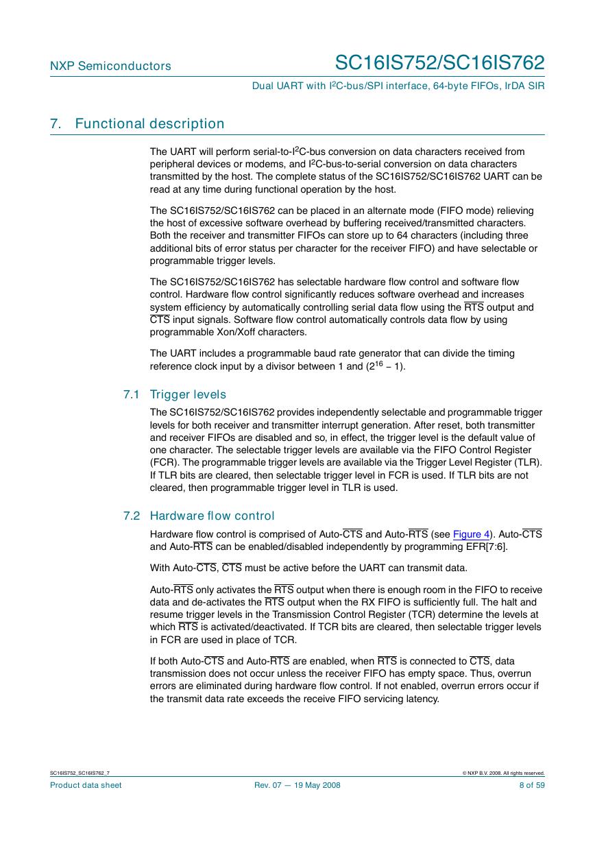
7.2 Hardware flow control
Hardware flow control is comprised of Auto-CTS and Auto-RTS (see Figure 4). Auto-CTS
and Auto-RTS can be enabled/disabled independently by programming EFR[7:6].
With Auto-CTS, CTS must be active before the UART can transmit data.
Auto-RTS only activates the RTS output when there is enough room in the FIFO to receive
data and de-activates the RTS output when the RX FIFO is sufficiently full. The halt and
resume trigger levels in the Transmission Control Register (TCR) determine the levels at
which RTS is activated/deactivated. If TCR bits are cleared, then selectable trigger levels
in FCR are used in place of TCR.
If both Auto-CTS and Auto-RTS are enabled, when RTS is connected to CTS, data
transmission does not occur unless the receiver FIFO has empty space. Thus, overrun
errors are eliminated during hardware flow control. If not enabled, overrun errors occur if
the transmit data rate exceeds the receive FIFO servicing latency.
SC16IS752_SC16IS762_7
Product data sheet
Rev. 07 — 19 May 2008
© NXP B.V. 2008. All rights reserved.
8 of 59
�



 V2版本原理图(Capacitive-Fingerprint-Reader-Schematic_V2).pdf
 摄像头工作原理.doc
 VL53L0X简要说明(En.FLVL53L00216).pdf
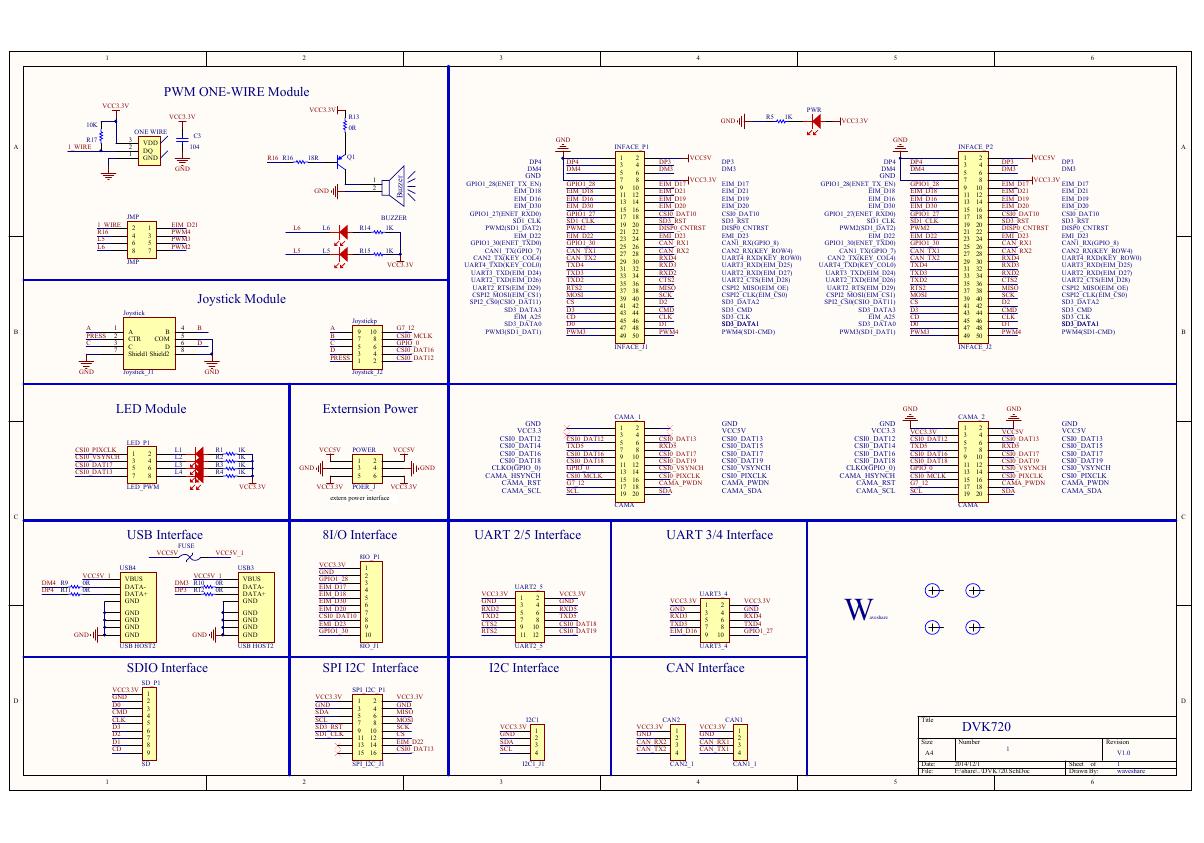 原理图(DVK720-Schematic).pdf
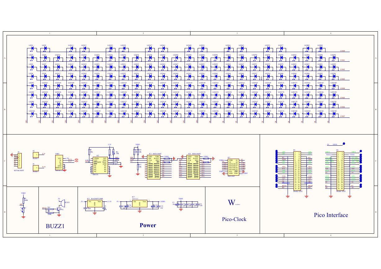 原理图(Pico-Clock-Green-Schdoc).pdf
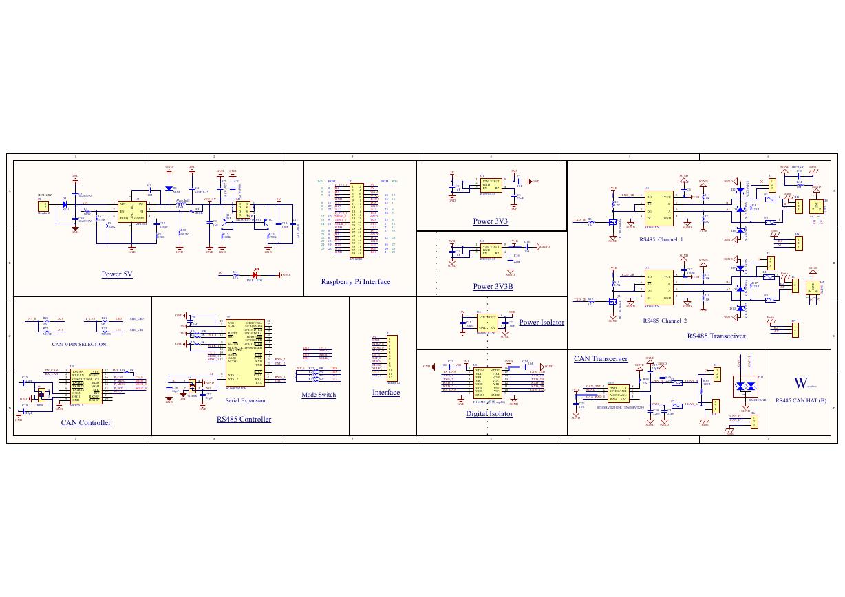 原理图(RS485-CAN-HAT-B-schematic).pdf
 File:SIM7500_SIM7600_SIM7800 Series_SSL_Application Note_V2.00.pdf
 ADS1263(Ads1262).pdf
 原理图(Open429Z-D-Schematic).pdf
 用户手册(Capacitive_Fingerprint_Reader_User_Manual_CN).pdf
 CY7C68013A(英文版)(CY7C68013A).pdf
 TechnicalReference_Dem.pdf