High Performance Stereo Audio DAC
ES8156
APPLICATIONS
• Headphone
• Speaker
• TV
• Portable audio devices
ORDERING INFORMATION
ES8156 -40°C ~ +85°C
QFN-20
FEATURES
• High performance and low power multi-
bit delta-sigma audio DAC
• 110 dB signal to noise ratio, -80 dB
THD+N
• 24-bit, 8 to 96 kHz sampling frequency
•
Integrated headphone driver with
capless option
• Differential output for higher SNR and
CMRR
I2S/PCM master or slave serial data port
•
• 256/384Fs, USB 12/24 MHz and other
non standard audio system clocks
I2C interface
•
• 7-band fully adjustable EQ
• Dynamic range compression
• Playback signal feedback
• Pop and click noise suppression
• 1.8V to 3.3V operation
1
�
Everest Semiconductor
Confidential
ES8156
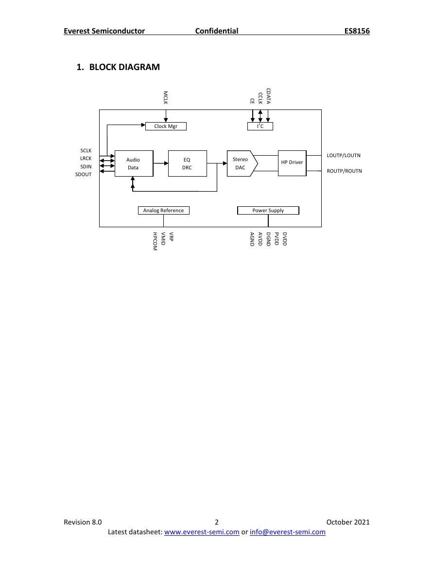
1. BLOCK DIAGRAM
M
C
L
K
Clock Mgr
C
D
A
T
A
C
C
L
K
C
E
I2C
SCLK
LRCK
SDIN
SDOUT
Audio
Data
EQ
DRC
Stereo
DAC
HP Driver
LOUTP/LOUTN
ROUTP/ROUTN
Analog Reference
V
R
P
V
M
D
I
H
P
C
O
M
Power Supply
A
G
N
D
A
V
D
D
D
G
N
D
P
V
D
D
D
V
D
D
Revision 8.0
Latest datasheet: www.everest-semi.com or info@everest-semi.com
2
October 2021
�
Everest Semiconductor
Confidential
ES8156
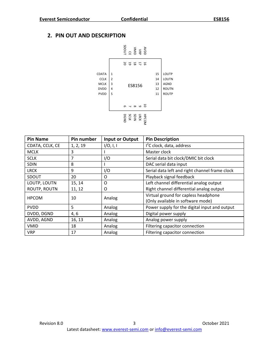
2. PIN OUT AND DESCRIPTION
S
D
O
U
T
V
M
D
I
V
R
P
A
V
D
D
C
E
2
0
1
9
1
8
1
7
1
6
Pin Name
CDATA, CCLK, CE
MCLK
SCLK
SDIN
LRCK
SDOUT
LOUTP, LOUTN
ROUTP, ROUTN
HPCOM
PVDD
DVDD, DGND
AVDD, AGND
VMID
VRP
CDATA
CCLK
MCLK
DVDD
PVDD
1
2
3
4
5
ES8156
6
7
8
9
1
0
15
14
13
12
11
LOUTP
LOUTN
AGND
ROUTN
ROUTP
S
C
L
K
D
G
N
D
S
D
N
I
L
R
C
K
H
P
C
O
M
Pin number
1, 2, 19
3
7
8
9
20
15, 14
11, 12
10
5
4, 6
16, 13
18
17
Input or Output
I/O, I, I
I
I/O
I
I/O
O
O
O
Analog
Analog
Analog
Analog
Analog
Analog
Pin Description
I2C clock, data, address
Master clock
Serial data bit clock/DMIC bit clock
DAC serial data input
Serial data left and right channel frame clock
Playback signal feedback
Left channel differential analog output
Right channel differential analog output
Virtual ground for capless headphone
(Only available in software mode)
Power supply for the digital input and output
Digital power supply
Analog power supply
Filtering capacitor connection
Filtering capacitor connection
Revision 8.0
Latest datasheet: www.everest-semi.com or info@everest-semi.com
3
October 2021
�
Everest Semiconductor
Confidential
ES8156
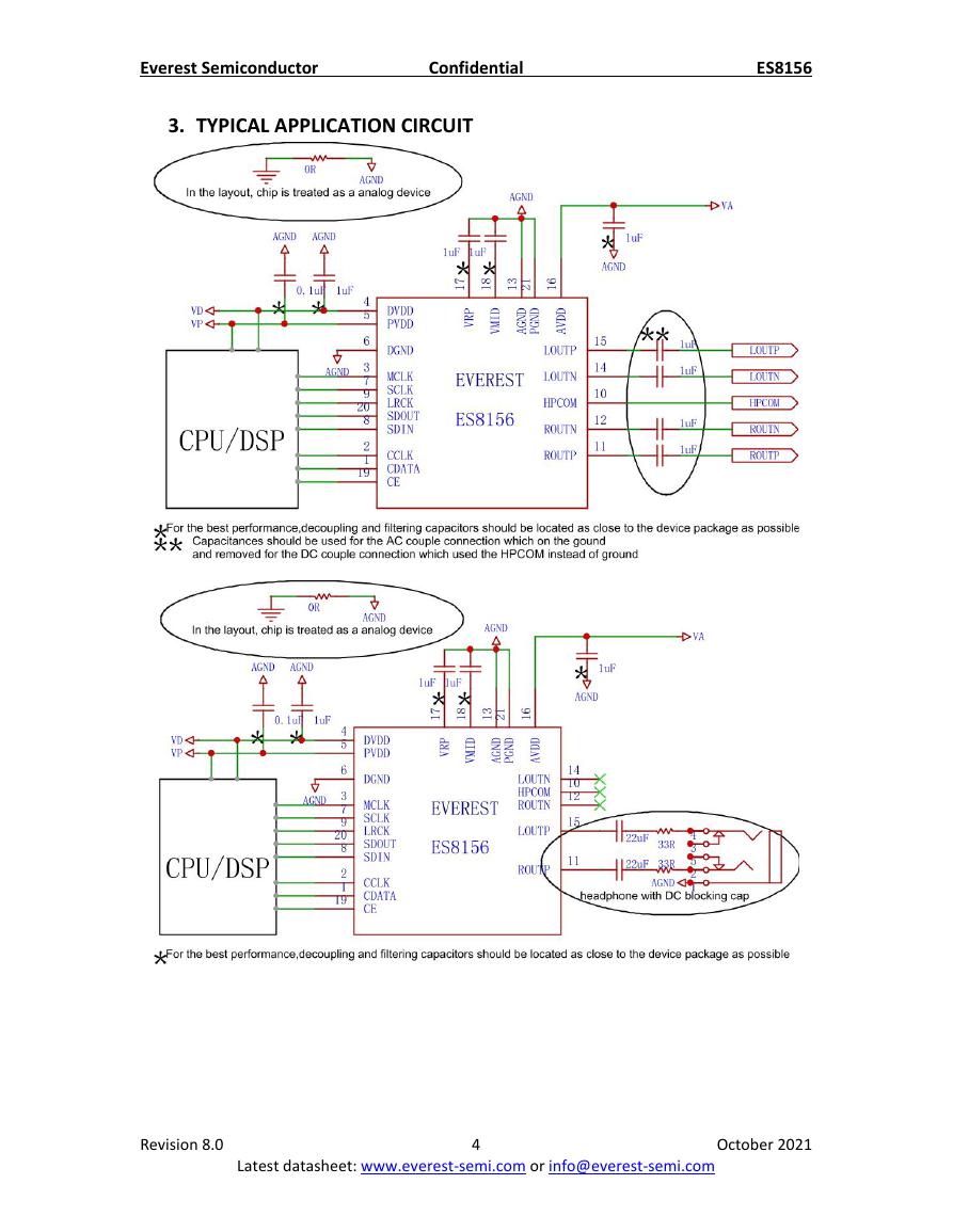
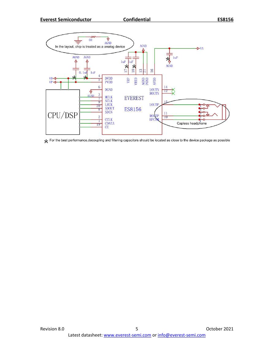
3. TYPICAL APPLICATION CIRCUIT
Revision 8.0
Latest datasheet: www.everest-semi.com or info@everest-semi.com
4
October 2021
�
Everest Semiconductor
Confidential
ES8156
Revision 8.0
Latest datasheet: www.everest-semi.com or info@everest-semi.com
5
October 2021
�
Everest Semiconductor
Confidential
ES8156
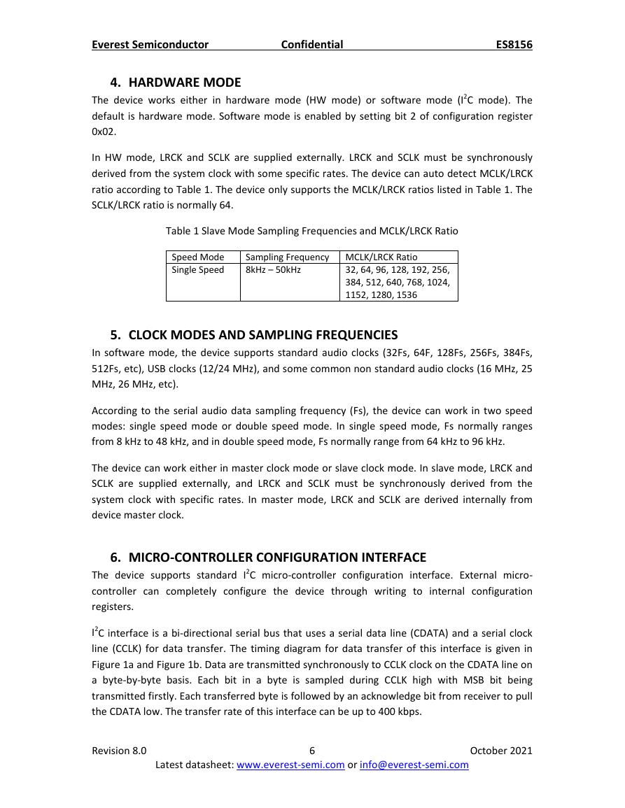
4. HARDWARE MODE
The device works either in hardware mode (HW mode) or software mode (I2C mode). The
default is hardware mode. Software mode is enabled by setting bit 2 of configuration register
0x02.
In HW mode, LRCK and SCLK are supplied externally. LRCK and SCLK must be synchronously
derived from the system clock with some specific rates. The device can auto detect MCLK/LRCK
ratio according to Table 1. The device only supports the MCLK/LRCK ratios listed in Table 1. The
SCLK/LRCK ratio is normally 64.
Table 1 Slave Mode Sampling Frequencies and MCLK/LRCK Ratio
Speed Mode
Single Speed
Sampling Frequency MCLK/LRCK Ratio
8kHz – 50kHz
32, 64, 96, 128, 192, 256,
384, 512, 640, 768, 1024,
1152, 1280, 1536
5. CLOCK MODES AND SAMPLING FREQUENCIES
In software mode, the device supports standard audio clocks (32Fs, 64F, 128Fs, 256Fs, 384Fs,
512Fs, etc), USB clocks (12/24 MHz), and some common non standard audio clocks (16 MHz, 25
MHz, 26 MHz, etc).
According to the serial audio data sampling frequency (Fs), the device can work in two speed
modes: single speed mode or double speed mode. In single speed mode, Fs normally ranges
from 8 kHz to 48 kHz, and in double speed mode, Fs normally range from 64 kHz to 96 kHz.
The device can work either in master clock mode or slave clock mode. In slave mode, LRCK and
SCLK are supplied externally, and LRCK and SCLK must be synchronously derived from the
system clock with specific rates. In master mode, LRCK and SCLK are derived internally from
device master clock.
6. MICRO-CONTROLLER CONFIGURATION INTERFACE
The device supports standard I2C micro-controller configuration interface. External micro-
controller can completely configure the device through writing to internal configuration
registers.
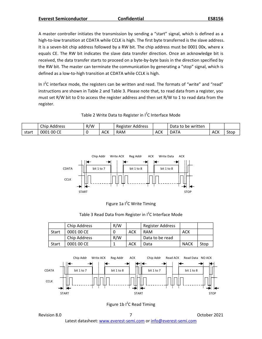
I2C interface is a bi-directional serial bus that uses a serial data line (CDATA) and a serial clock
line (CCLK) for data transfer. The timing diagram for data transfer of this interface is given in
Figure 1a and Figure 1b. Data are transmitted synchronously to CCLK clock on the CDATA line on
a byte-by-byte basis. Each bit in a byte is sampled during CCLK high with MSB bit being
transmitted firstly. Each transferred byte is followed by an acknowledge bit from receiver to pull
the CDATA low. The transfer rate of this interface can be up to 400 kbps.
Revision 8.0
Latest datasheet: www.everest-semi.com or info@everest-semi.com
6
October 2021
�
Everest Semiconductor
Confidential
ES8156
A master controller initiates the transmission by sending a “start” signal, which is defined as a
high-to-low transition at CDATA while CCLK is high. The first byte transferred is the slave address.
It is a seven-bit chip address followed by a RW bit. The chip address must be 0001 00x, where x
equals CE. The RW bit indicates the slave data transfer direction. Once an acknowledge bit is
received, the data transfer starts to proceed on a byte-by-byte basis in the direction specified by
the RW bit. The master can terminate the communication by generating a “stop” signal, which is
defined as a low-to-high transition at CDATA while CCLK is high.
In I2C interface mode, the registers can be written and read. The formats of “write” and “read”
instructions are shown in Table 2 and Table 3. Please note that, to read data from a register, you
must set R/W bit to 0 to access the register address and then set R/W to 1 to read data from the
register.
Table 2 Write Data to Register in I2C Interface Mode
start
Chip Address
0001 00 CE
R/W
0
ACK
Register Address
RAM
ACK
Data to be written
DATA
ACK
Stop
ACK
Write Data
ACK
bit 1 to 8
Chip Addr
Write ACK
bit 1 to 7
Reg Addr
bit 1 to 8
CDATA
CCLK
START
Figure 1a I2C Write Timing
Table 3 Read Data from Register in I2C Interface Mode
STOP
Start
Start
Chip Address
0001 00 CE
Chip Address
0001 00 CE
R/W
0
R/W
1
Register Address
RAM
Data to be read
Data
ACK
NACK
Stop
Chip Addr
Write ACK
Reg Addr
bit 1 to 7
bit 1 to 8
Chip Addr
Read ACK
Read Data
NO ACK
bit 1 to 7
bit 1 to 8
Figure 1b I2C Read Timing
Latest datasheet: www.everest-semi.com or info@everest-semi.com
STOP
October 2021
ACK
ACK
ACK
START
7
CDATA
CCLK
START
Revision 8.0
�
Everest Semiconductor
Confidential
ES8156
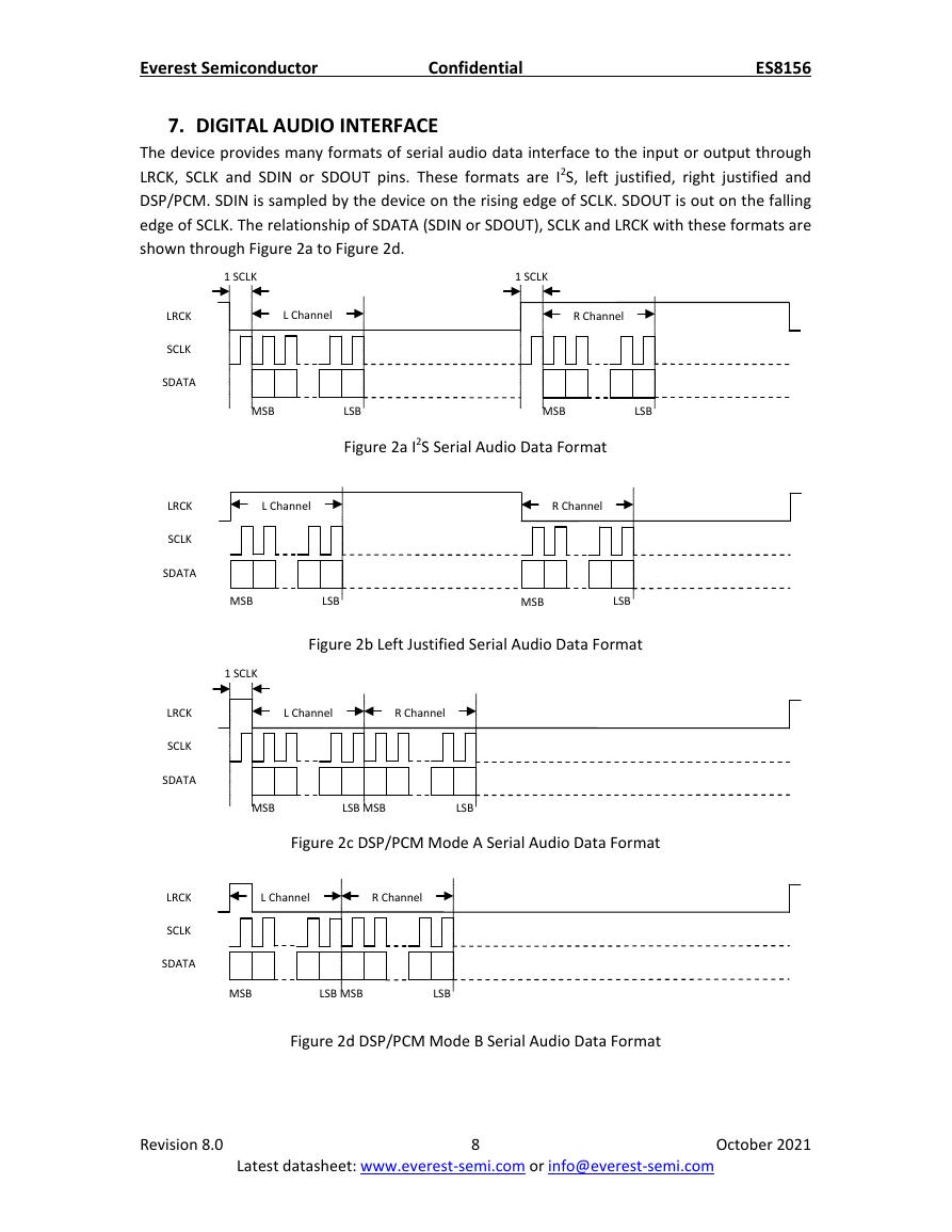
7. DIGITAL AUDIO INTERFACE
The device provides many formats of serial audio data interface to the input or output through
LRCK, SCLK and SDIN or SDOUT pins. These formats are I2S, left justified, right justified and
DSP/PCM. SDIN is sampled by the device on the rising edge of SCLK. SDOUT is out on the falling
edge of SCLK. The relationship of SDATA (SDIN or SDOUT), SCLK and LRCK with these formats are
shown through Figure 2a to Figure 2d.
LRCK
SCLK
SDATA
LRCK
SCLK
SDATA
LRCK
SCLK
SDATA
LRCK
SCLK
SDATA
1 SCLK
L Channel
MSB
LSB
1 SCLK
R Channel
MSB
LSB
Figure 2a I2S Serial Audio Data Format
L Channel
MSB
LSB
R Channel
MSB
LSB
Figure 2b Left Justified Serial Audio Data Format
1 SCLK
L Channel
R Channel
MSB
LSB MSB
LSB
Figure 2c DSP/PCM Mode A Serial Audio Data Format
L Channel
R Channel
MSB
LSB MSB
LSB
Figure 2d DSP/PCM Mode B Serial Audio Data Format
Revision 8.0
Latest datasheet: www.everest-semi.com or info@everest-semi.com
8
October 2021
�


 V2版本原理图(Capacitive-Fingerprint-Reader-Schematic_V2).pdf
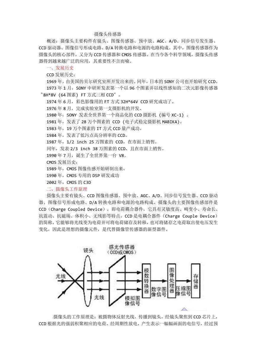 摄像头工作原理.doc
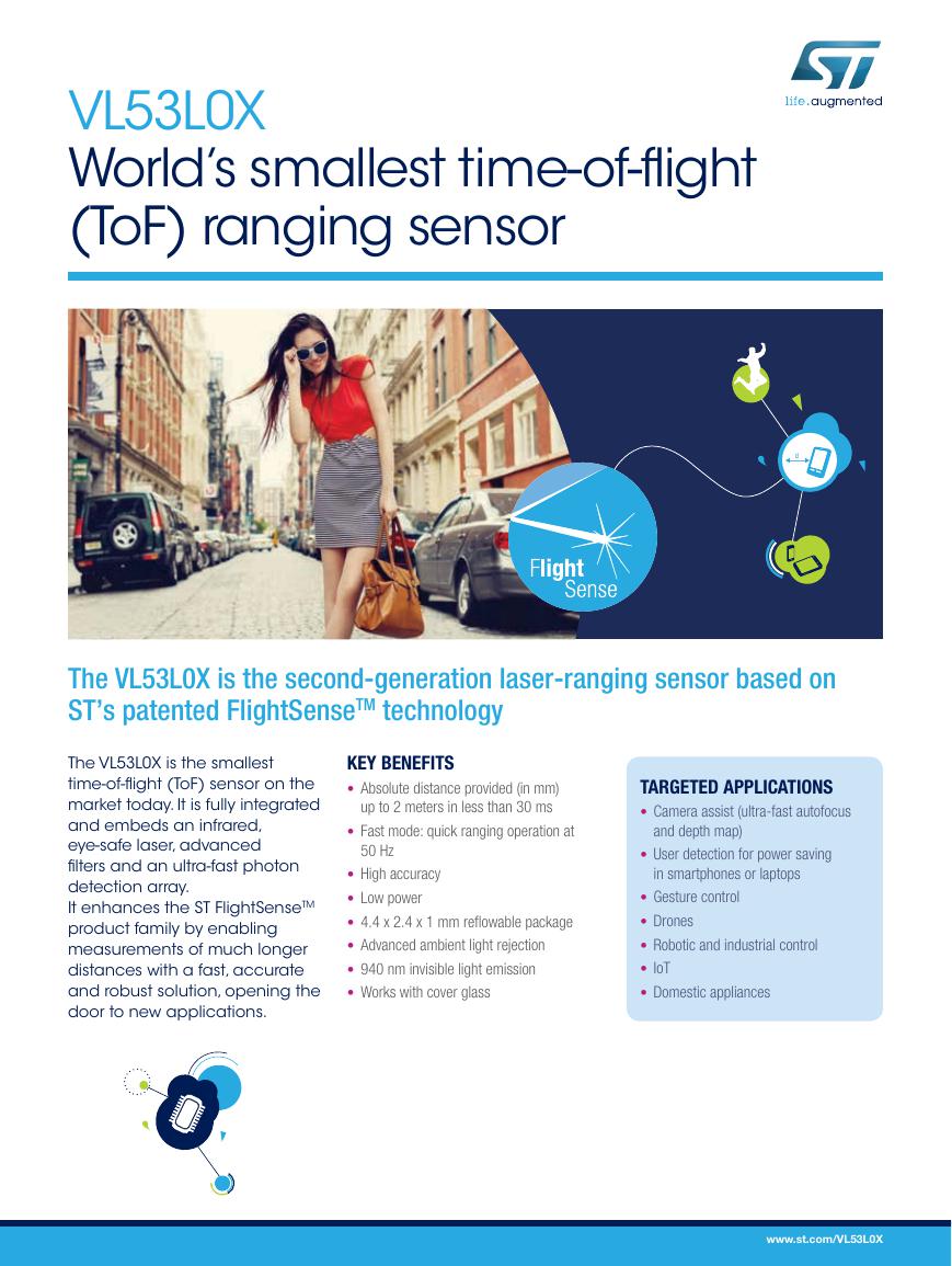 VL53L0X简要说明(En.FLVL53L00216).pdf
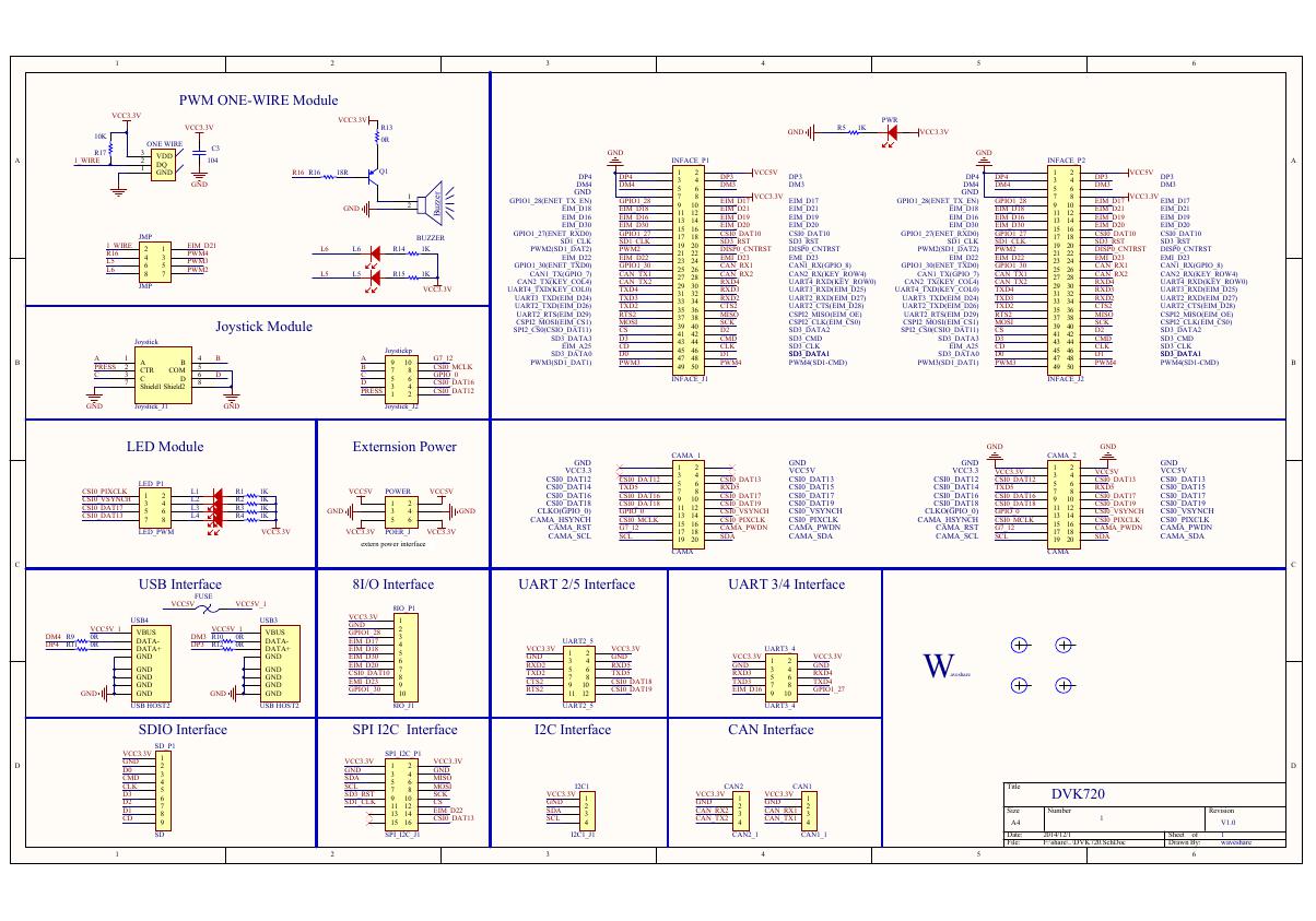 原理图(DVK720-Schematic).pdf
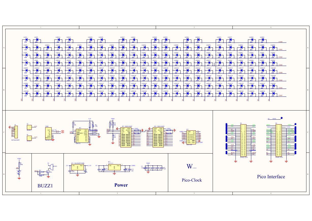 原理图(Pico-Clock-Green-Schdoc).pdf
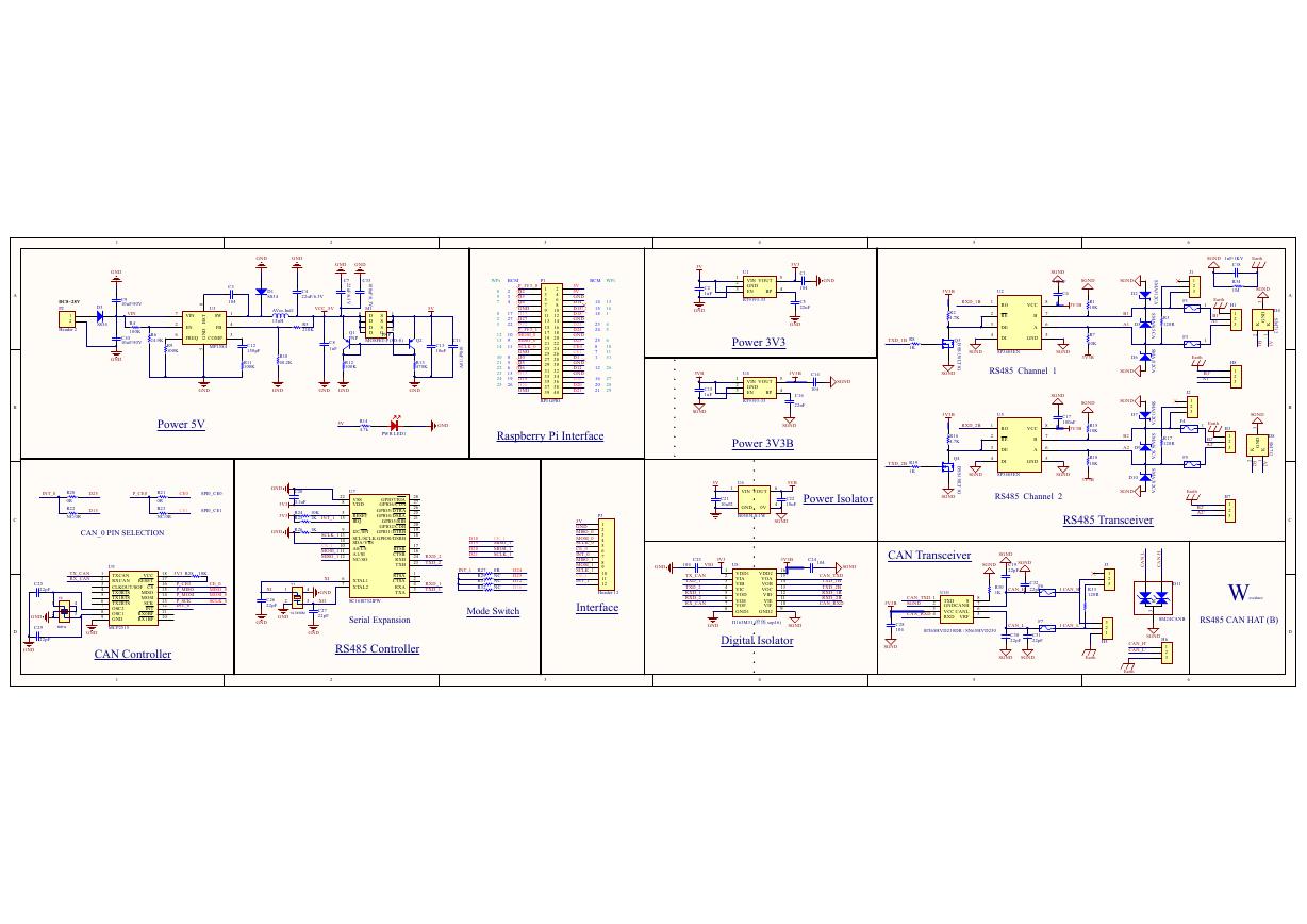 原理图(RS485-CAN-HAT-B-schematic).pdf
 File:SIM7500_SIM7600_SIM7800 Series_SSL_Application Note_V2.00.pdf
 ADS1263(Ads1262).pdf
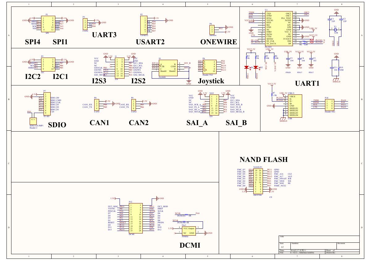 原理图(Open429Z-D-Schematic).pdf
 用户手册(Capacitive_Fingerprint_Reader_User_Manual_CN).pdf
 CY7C68013A(英文版)(CY7C68013A).pdf
 TechnicalReference_Dem.pdf