NTAG213/215/216
NFC Forum Type 2 Tag compliant IC with 144/504/888 bytes
user memory
Rev. 3.2 — 2 June 2015
265332
Product data sheet
COMPANY PUBLIC
1. General description
NTAG213, NTAG215 and NTAG216 have been developed by NXP Semiconductors as
standard NFC tag ICs to be used in mass market applications such as retail, gaming and
consumer electronics, in combination with NFC devices or NFC compliant Proximity
Coupling Devices. NTAG213, NTAG215 and NTAG216 (from now on, generally called
NTAG21x) are designed to fully comply to NFC Forum Type 2 Tag (Ref. 2) and
ISO/IEC14443 Type A (Ref. 1) specifications.
Target applications include Out-of-Home and print media smart advertisement, SoLoMo
applications, product authentication, NFC shelf labels, mobile companion tags.
Target use cases include Out-of-Home smart advertisement, product authentication,
mobile companion tags, Bluetooth or Wi-Fi pairing, electronic shelf labels and business
cards. NTAG21x memory can also be segmented to implement multiple applications at
the same time.
Thanks to the high input capacitance, NTAG21x tag ICs are particularly tailored for
applications requiring small footprints, without compromise on performance. Small NFC
tags can be more easily embedded into e.g. product labels or electronic devices.
The mechanical and electrical specifications of NTAG21x are tailored to meet the
requirements of inlay and tag manufacturers.
1.1 Contactless energy and data transfer
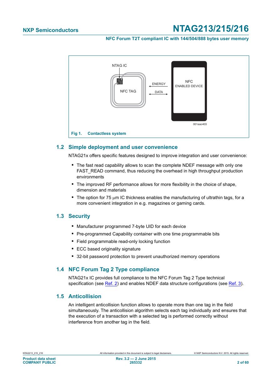
Communication to NTAG21x can be established only when the IC is connected to an
antenna. Form and specification of the coil is out of scope of this document.
When NTAG21x is positioned in the RF field, the high speed RF communication interface
allows the transmission of the data with a baud rate of 106 kbit/s.
�
NXP Semiconductors
NFC Forum T2T compliant IC with 144/504/888 bytes user memory
NTAG213/215/216
NTAG IC
NFC TAG
ENERGY
DATA
NFC
ENABLED DEVICE
Fig 1. Contactless system
1.2 Simple deployment and user convenience
001aao403
NTAG21x offers specific features designed to improve integration and user convenience:
• The fast read capability allows to scan the complete NDEF message with only one
FAST_READ command, thus reducing the overhead in high throughput production
environments
• The improved RF performance allows for more flexibility in the choice of shape,
dimension and materials
• The option for 75 m IC thickness enables the manufacturing of ultrathin tags, for a
more convenient integration in e.g. magazines or gaming cards.
1.3 Security
• Manufacturer programmed 7-byte UID for each device
• Pre-programmed Capability container with one time programmable bits
• Field programmable read-only locking function
• ECC based originality signature
• 32-bit password protection to prevent unauthorized memory operations
1.4 NFC Forum Tag 2 Type compliance
NTAG21x IC provides full compliance to the NFC Forum Tag 2 Type technical
specification (see Ref. 2) and enables NDEF data structure configurations (see Ref. 3).
1.5 Anticollision
An intelligent anticollision function allows to operate more than one tag in the field
simultaneously. The anticollision algorithm selects each tag individually and ensures that
the execution of a transaction with a selected tag is performed correctly without
interference from another tag in the field.
NTAG213_215_216
Product data sheet
COMPANY PUBLIC
All information provided in this document is subject to legal disclaimers.
© NXP Semiconductors N.V. 2015. All rights reserved.
Rev. 3.2 — 2 June 2015
265332
2 of 60
�
NXP Semiconductors
NFC Forum T2T compliant IC with 144/504/888 bytes user memory
NTAG213/215/216
2. Features and benefits
Contactless transmission of data and supply energy
Operating frequency of 13.56 MHz
Data transfer of 106 kbit/s
Data integrity of 16-bit CRC, parity, bit coding, bit counting
Operating distance up to 100 mm (depending on various parameters as e.g. field
strength and antenna geometry)
7-byte serial number (cascade level 2 according to ISO/IEC 14443-3)
UID ASCII mirror for automatic serialization of NDEF messages
Automatic NFC counter triggered at read command
NFC counter ASCII mirror for automatic adding the NFC counter value to the NDEF
message
ECC based originality signature
Fast read command
True anticollision
50 pF input capacitance
2.1 EEPROM
180, 540 or 924 bytes organized in 45, 135 or 231 pages with 4 bytes per page
144, 504 or 888 bytes freely available user Read/Write area (36, 126 or 222 pages)
4 bytes initialized capability container with one time programmable access bits
Field programmable read-only locking function per page for the first 16 pages
Field programmable read-only locking function above the first 16 pages per double
page for NTAG213 or per 16 pages for NTAG215 and NTAG216
Configurable password protection with optional limit of unsuccessful attempts
Anti-tearing support for capability container (CC) and lock bits
ECC supported originality check
Data retention time of 10 years
Write endurance 100.000 cycles
3. Applications
Smart advertisement
Goods and device authentication
Call request
SMS
Call to action
Voucher and coupons
Bluetooth or Wi-Fi pairing
Connection handover
Product authentication
Mobile companion tags
Electronic shelf labels
Business cards
NTAG213_215_216
Product data sheet
COMPANY PUBLIC
All information provided in this document is subject to legal disclaimers.
© NXP Semiconductors N.V. 2015. All rights reserved.
Rev. 3.2 — 2 June 2015
265332
3 of 60
�
NXP Semiconductors
NFC Forum T2T compliant IC with 144/504/888 bytes user memory
NTAG213/215/216
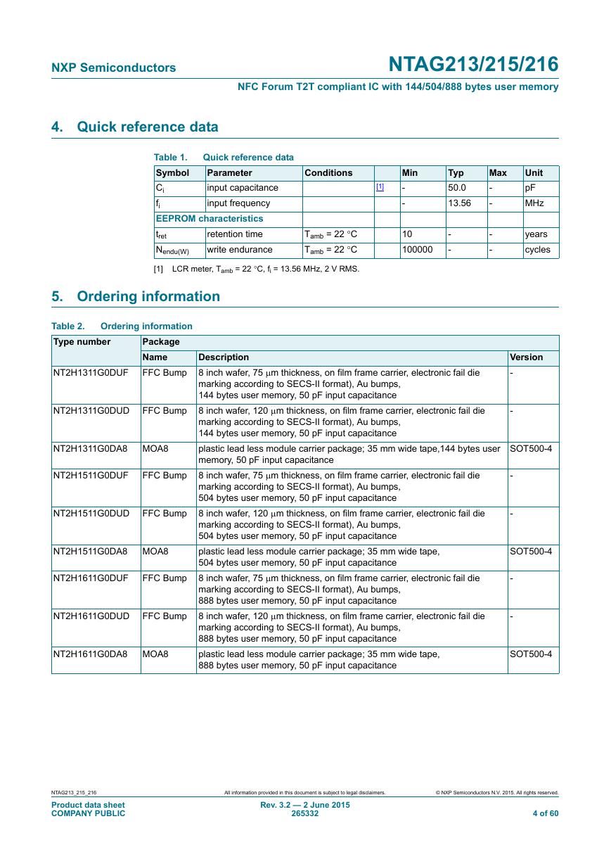
4. Quick reference data
Quick reference data
Parameter
input capacitance
input frequency
Table 1.
Symbol
Ci
fi
EEPROM characteristics
retention time
tret
write endurance
Nendu(W)
[1]
Tamb = 22 C
Tamb = 22 C
LCR meter, Tamb = 22 C, fi = 13.56 MHz, 2 V RMS.
Conditions
[1]
Min
-
-
Typ
50.0
13.56
10
100000
-
-
Max
-
-
-
-
Unit
pF
MHz
years
cycles
5. Ordering information
Table 2.
Type number
Ordering information
Package
Name
FFC Bump
NT2H1311G0DUF
NT2H1311G0DUD FFC Bump
NT2H1311G0DA8 MOA8
NT2H1511G0DUF
FFC Bump
NT2H1511G0DUD FFC Bump
NT2H1511G0DA8 MOA8
NT2H1611G0DUF
FFC Bump
NT2H1611G0DUD FFC Bump
NT2H1611G0DA8 MOA8
Description
8 inch wafer, 75 m thickness, on film frame carrier, electronic fail die
marking according to SECS-II format), Au bumps,
144 bytes user memory, 50 pF input capacitance
8 inch wafer, 120 m thickness, on film frame carrier, electronic fail die
marking according to SECS-II format), Au bumps,
144 bytes user memory, 50 pF input capacitance
plastic lead less module carrier package; 35 mm wide tape,144 bytes user
memory, 50 pF input capacitance
8 inch wafer, 75 m thickness, on film frame carrier, electronic fail die
marking according to SECS-II format), Au bumps,
504 bytes user memory, 50 pF input capacitance
8 inch wafer, 120 m thickness, on film frame carrier, electronic fail die
marking according to SECS-II format), Au bumps,
504 bytes user memory, 50 pF input capacitance
plastic lead less module carrier package; 35 mm wide tape,
504 bytes user memory, 50 pF input capacitance
8 inch wafer, 75 m thickness, on film frame carrier, electronic fail die
marking according to SECS-II format), Au bumps,
888 bytes user memory, 50 pF input capacitance
8 inch wafer, 120 m thickness, on film frame carrier, electronic fail die
marking according to SECS-II format), Au bumps,
888 bytes user memory, 50 pF input capacitance
plastic lead less module carrier package; 35 mm wide tape,
888 bytes user memory, 50 pF input capacitance
Version
-
-
SOT500-4
-
-
SOT500-4
-
-
SOT500-4
NTAG213_215_216
Product data sheet
COMPANY PUBLIC
All information provided in this document is subject to legal disclaimers.
© NXP Semiconductors N.V. 2015. All rights reserved.
Rev. 3.2 — 2 June 2015
265332
4 of 60
�
NFC Forum T2T compliant IC with 144/504/888 bytes user memory
NTAG213/215/216
NXP Semiconductors
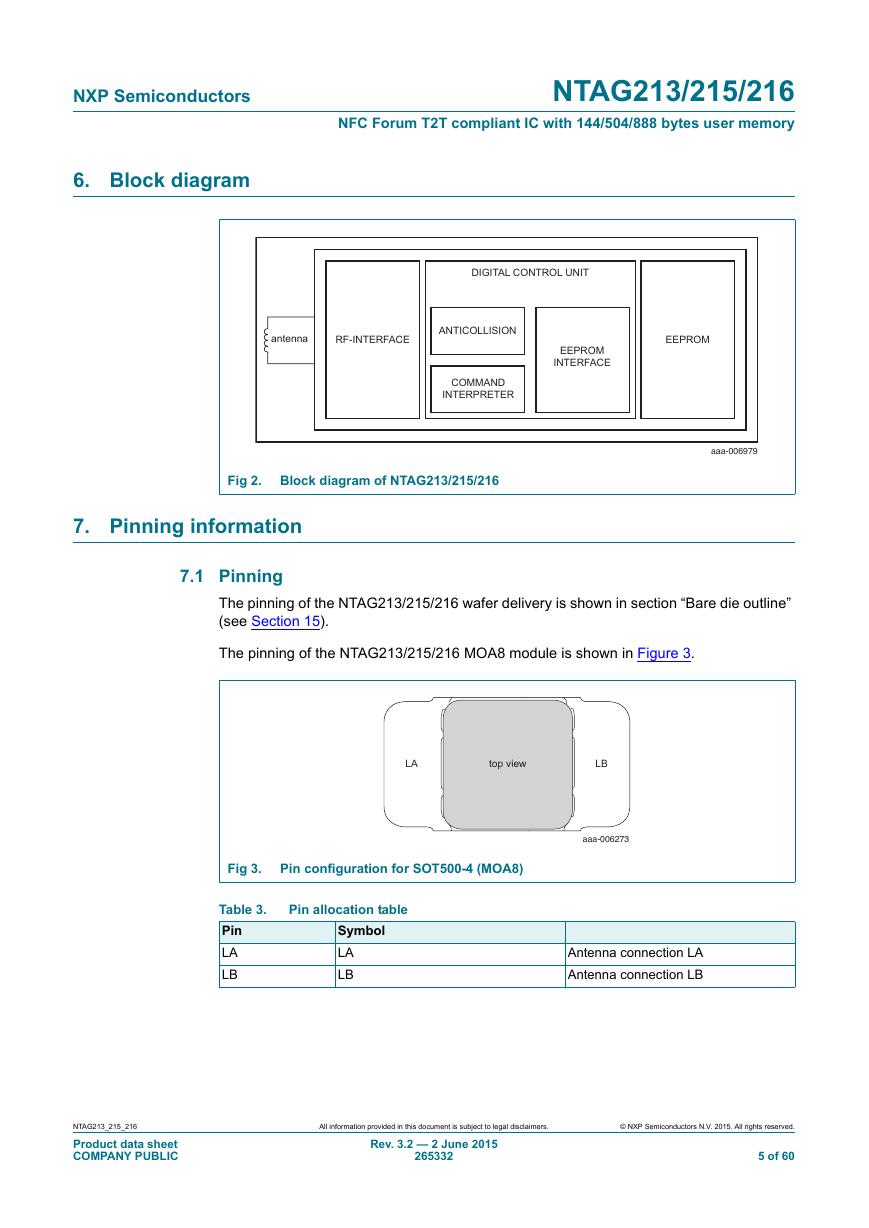
6. Block diagram
DIGITAL CONTROL UNIT
antenna
RF-INTERFACE
ANTICOLLISION
EEPROM
INTERFACE
EEPROM
COMMAND
INTERPRETER
Fig 2. Block diagram of NTAG213/215/216
aaa-006979
7. Pinning information
7.1 Pinning
The pinning of the NTAG213/215/216 wafer delivery is shown in section “Bare die outline”
(see Section 15).
The pinning of the NTAG213/215/216 MOA8 module is shown in Figure 3.
LA
top view
LB
Fig 3.
Pin configuration for SOT500-4 (MOA8)
aaa-006273
Table 3.
Pin
LA
LB
Pin allocation table
Symbol
LA
LB
Antenna connection LA
Antenna connection LB
NTAG213_215_216
Product data sheet
COMPANY PUBLIC
All information provided in this document is subject to legal disclaimers.
© NXP Semiconductors N.V. 2015. All rights reserved.
Rev. 3.2 — 2 June 2015
265332
5 of 60
�
NXP Semiconductors
NFC Forum T2T compliant IC with 144/504/888 bytes user memory
NTAG213/215/216
8. Functional description
8.1 Block description
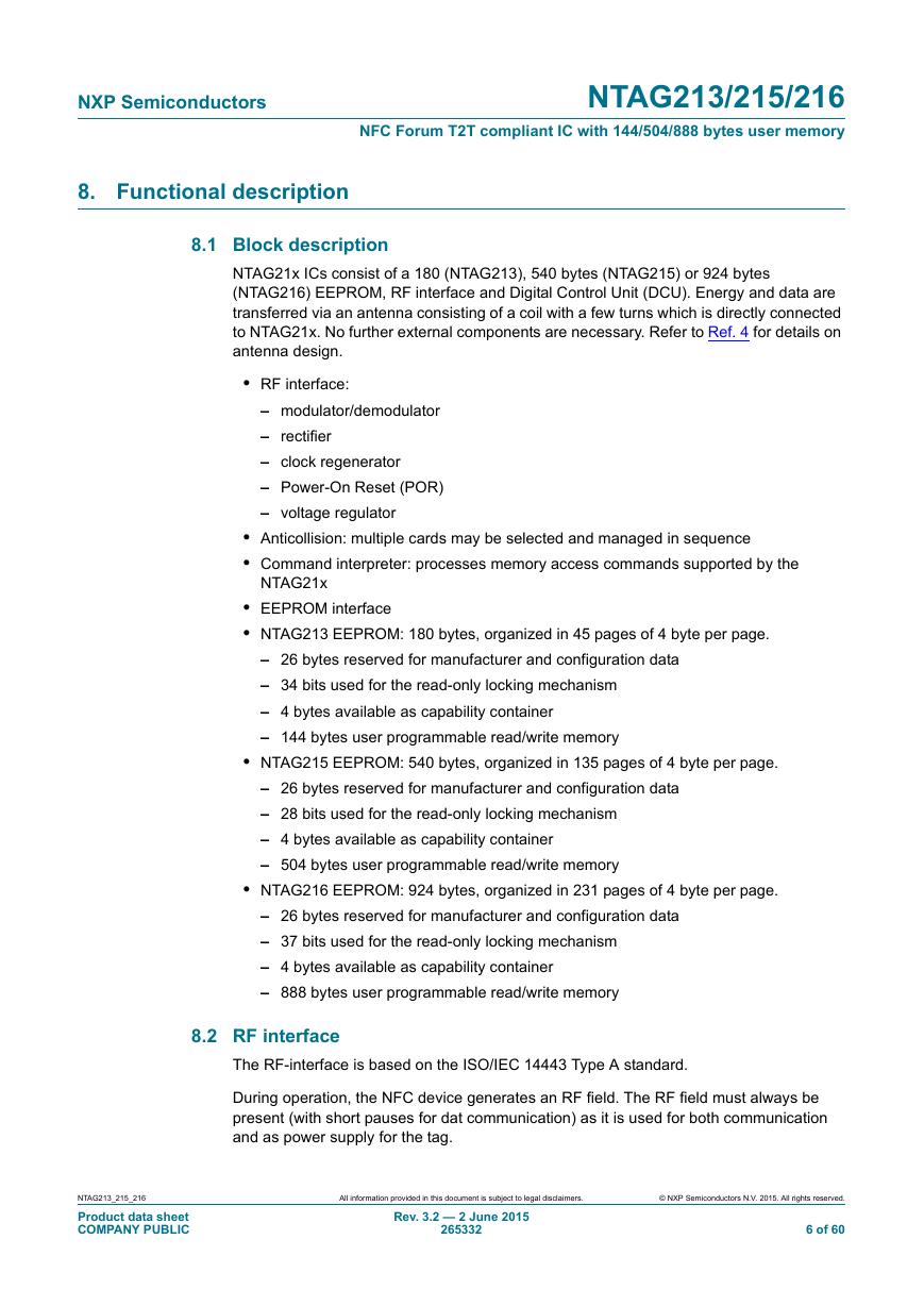
NTAG21x ICs consist of a 180 (NTAG213), 540 bytes (NTAG215) or 924 bytes
(NTAG216) EEPROM, RF interface and Digital Control Unit (DCU). Energy and data are
transferred via an antenna consisting of a coil with a few turns which is directly connected
to NTAG21x. No further external components are necessary. Refer to Ref. 4 for details on
antenna design.
• RF interface:
– modulator/demodulator
– rectifier
– clock regenerator
– Power-On Reset (POR)
– voltage regulator
• Anticollision: multiple cards may be selected and managed in sequence
• Command interpreter: processes memory access commands supported by the
NTAG21x
• EEPROM interface
• NTAG213 EEPROM: 180 bytes, organized in 45 pages of 4 byte per page.
– 26 bytes reserved for manufacturer and configuration data
– 34 bits used for the read-only locking mechanism
– 4 bytes available as capability container
– 144 bytes user programmable read/write memory
• NTAG215 EEPROM: 540 bytes, organized in 135 pages of 4 byte per page.
– 26 bytes reserved for manufacturer and configuration data
– 28 bits used for the read-only locking mechanism
– 4 bytes available as capability container
– 504 bytes user programmable read/write memory
• NTAG216 EEPROM: 924 bytes, organized in 231 pages of 4 byte per page.
– 26 bytes reserved for manufacturer and configuration data
– 37 bits used for the read-only locking mechanism
– 4 bytes available as capability container
– 888 bytes user programmable read/write memory
8.2 RF interface
The RF-interface is based on the ISO/IEC 14443 Type A standard.
During operation, the NFC device generates an RF field. The RF field must always be
present (with short pauses for dat communication) as it is used for both communication
and as power supply for the tag.
NTAG213_215_216
Product data sheet
COMPANY PUBLIC
All information provided in this document is subject to legal disclaimers.
© NXP Semiconductors N.V. 2015. All rights reserved.
Rev. 3.2 — 2 June 2015
265332
6 of 60
�
NXP Semiconductors
NFC Forum T2T compliant IC with 144/504/888 bytes user memory
NTAG213/215/216
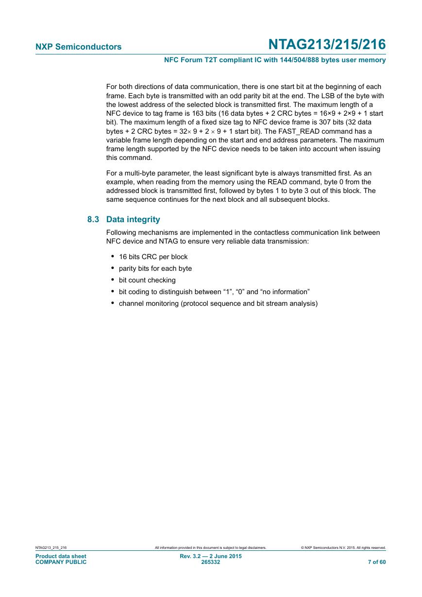
For both directions of data communication, there is one start bit at the beginning of each
frame. Each byte is transmitted with an odd parity bit at the end. The LSB of the byte with
the lowest address of the selected block is transmitted first. The maximum length of a
NFC device to tag frame is 163 bits (16 data bytes + 2 CRC bytes = 16×9 + 2×9 + 1 start
bit). The maximum length of a fixed size tag to NFC device frame is 307 bits (32 data
bytes + 2 CRC bytes = 32 9 + 2 9 + 1 start bit). The FAST_READ command has a
variable frame length depending on the start and end address parameters. The maximum
frame length supported by the NFC device needs to be taken into account when issuing
this command.
For a multi-byte parameter, the least significant byte is always transmitted first. As an
example, when reading from the memory using the READ command, byte 0 from the
addressed block is transmitted first, followed by bytes 1 to byte 3 out of this block. The
same sequence continues for the next block and all subsequent blocks.
8.3 Data integrity
Following mechanisms are implemented in the contactless communication link between
NFC device and NTAG to ensure very reliable data transmission:
• 16 bits CRC per block
• parity bits for each byte
• bit count checking
• bit coding to distinguish between “1”, “0” and “no information”
• channel monitoring (protocol sequence and bit stream analysis)
NTAG213_215_216
Product data sheet
COMPANY PUBLIC
All information provided in this document is subject to legal disclaimers.
© NXP Semiconductors N.V. 2015. All rights reserved.
Rev. 3.2 — 2 June 2015
265332
7 of 60
�
NXP Semiconductors
NFC Forum T2T compliant IC with 144/504/888 bytes user memory
NTAG213/215/216
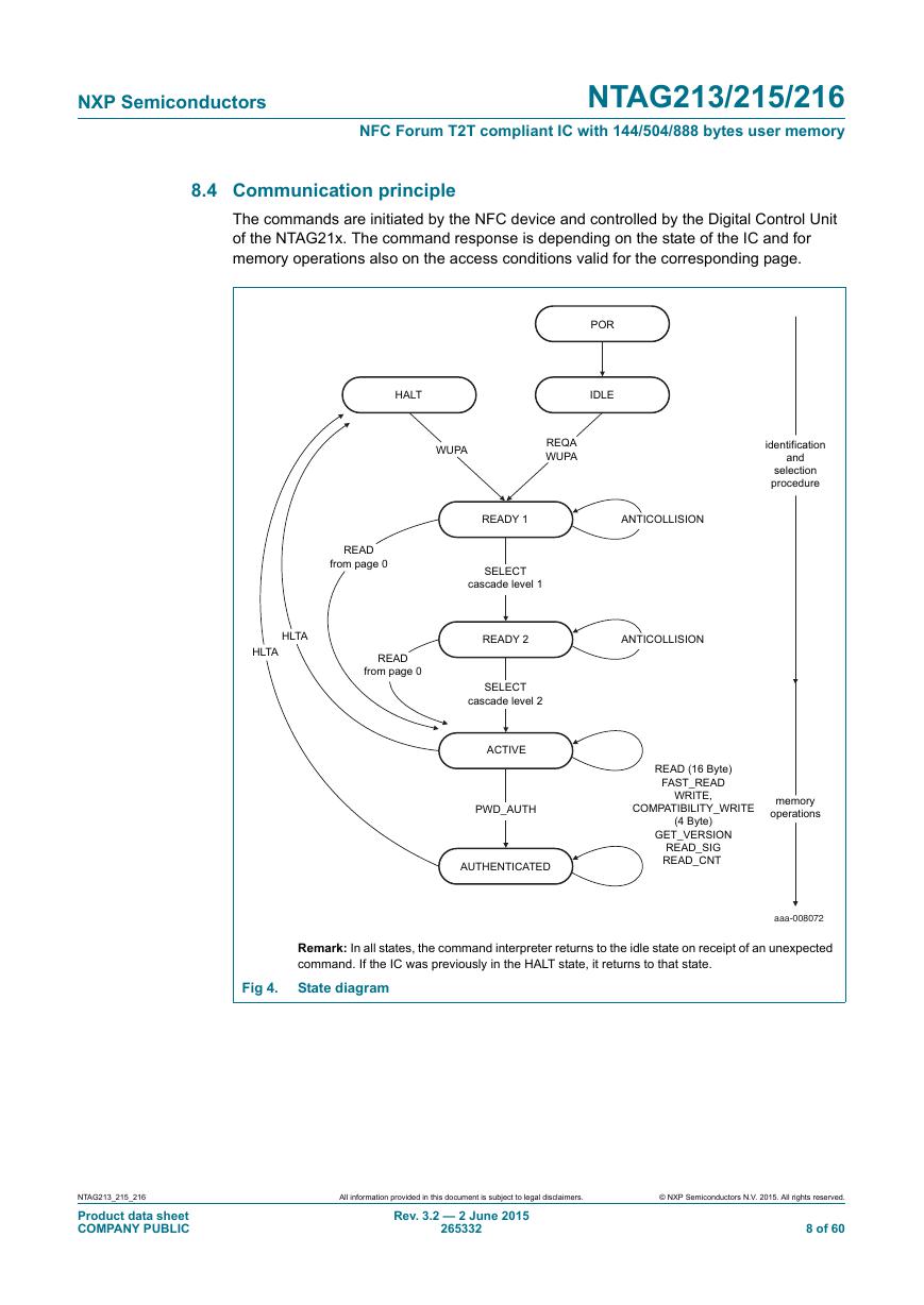
8.4 Communication principle
The commands are initiated by the NFC device and controlled by the Digital Control Unit
of the NTAG21x. The command response is depending on the state of the IC and for
memory operations also on the access conditions valid for the corresponding page.
POR
IDLE
HALT
WUPA
REQA
WUPA
READY 1
ANTICOLLISION
READ
from page 0
SELECT
cascade level 1
HLTA
HLTA
READ
from page 0
READY 2
ANTICOLLISION
SELECT
cascade level 2
ACTIVE
PWD_AUTH
AUTHENTICATED
READ (16 Byte)
FAST_READ
COMPATIBILITY_WRITE
WRITE,
(4 Byte)
GET_VERSION
READ_SIG
READ_CNT
identification
and
selection
procedure
memory
operations
aaa-008072
Remark: In all states, the command interpreter returns to the idle state on receipt of an unexpected
command. If the IC was previously in the HALT state, it returns to that state.
State diagram
Fig 4.
NTAG213_215_216
Product data sheet
COMPANY PUBLIC
All information provided in this document is subject to legal disclaimers.
© NXP Semiconductors N.V. 2015. All rights reserved.
Rev. 3.2 — 2 June 2015
265332
8 of 60
�



 V2版本原理图(Capacitive-Fingerprint-Reader-Schematic_V2).pdf
 摄像头工作原理.doc
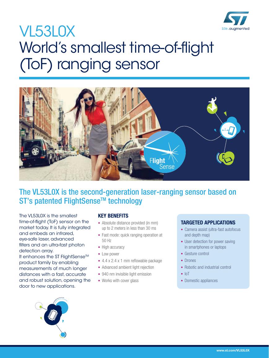 VL53L0X简要说明(En.FLVL53L00216).pdf
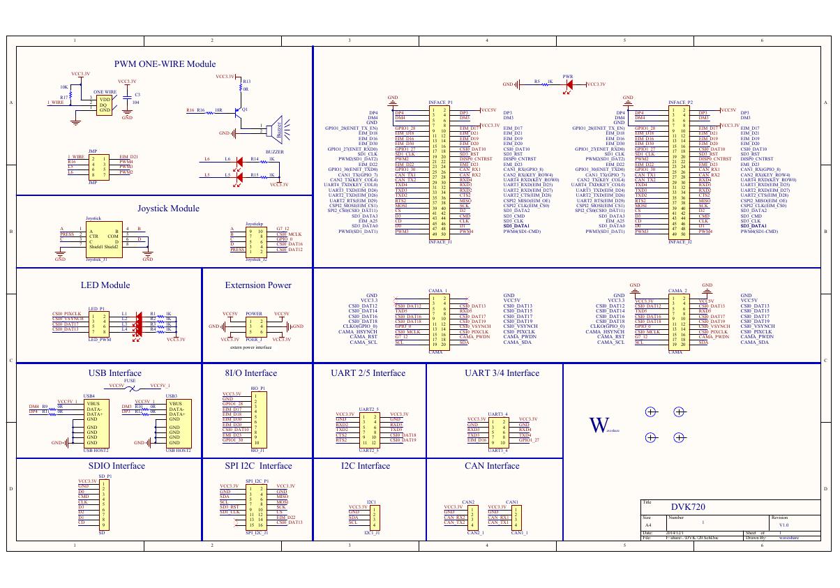 原理图(DVK720-Schematic).pdf
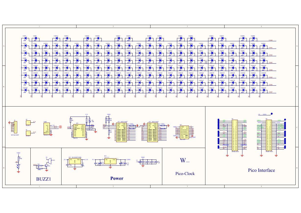 原理图(Pico-Clock-Green-Schdoc).pdf
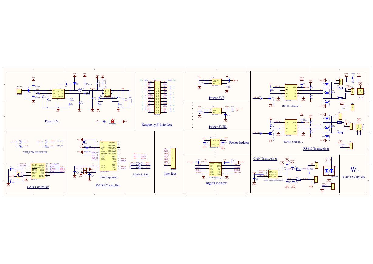 原理图(RS485-CAN-HAT-B-schematic).pdf
 File:SIM7500_SIM7600_SIM7800 Series_SSL_Application Note_V2.00.pdf
 ADS1263(Ads1262).pdf
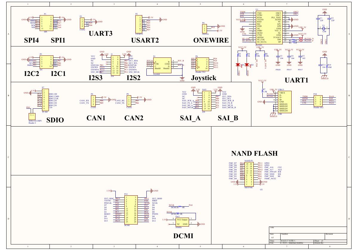 原理图(Open429Z-D-Schematic).pdf
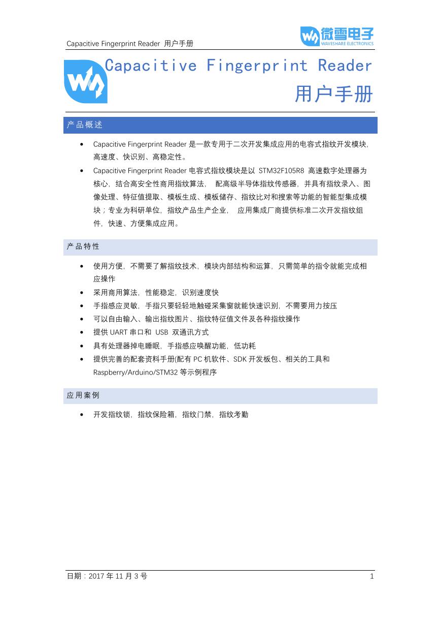 用户手册(Capacitive_Fingerprint_Reader_User_Manual_CN).pdf
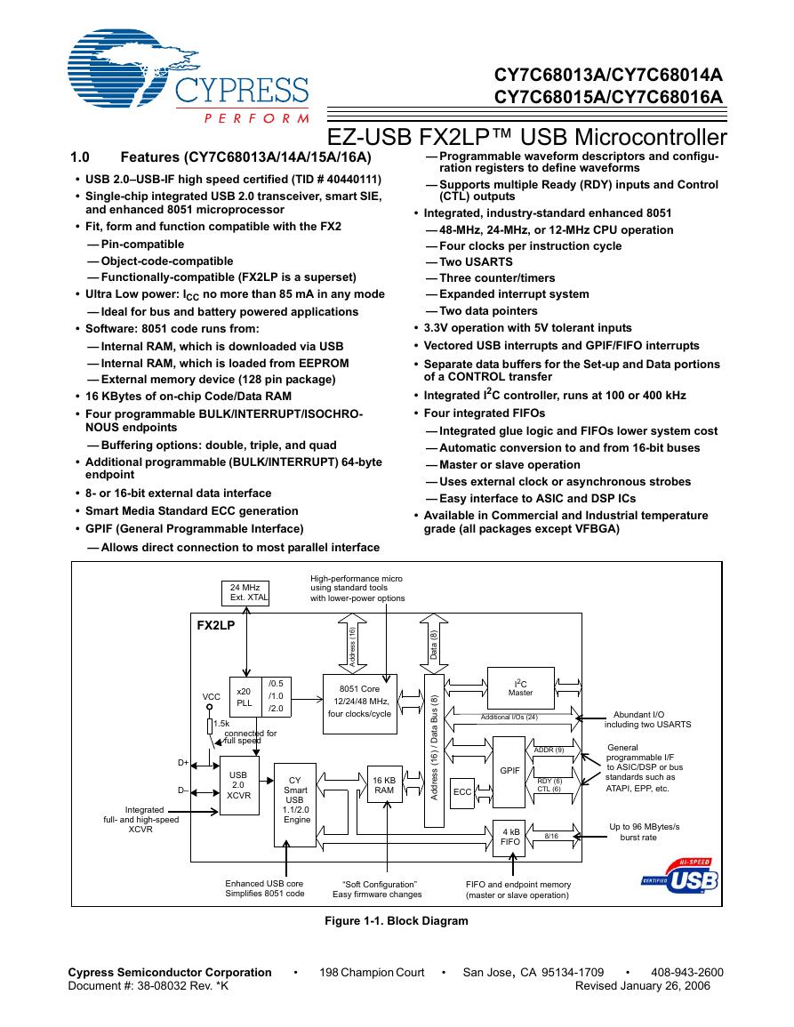 CY7C68013A(英文版)(CY7C68013A).pdf
 TechnicalReference_Dem.pdf