CP2102
SINGLE-CHIP USB TO UART BRIDGE
Single-Chip USB to UART Data Transfer
Virtual COM Port Device Drivers
Integrated USB transceiver; no external resistors
required
Integrated clock; no external crystal required
Integrated 1024-Byte EEPROM for vendor ID, product
ID, serial number, power descriptor, release number,
and product description strings
On-chip power-on reset circuit
On-chip voltage regulator: 3.3 V output
100% pin and software compatible with CP2101
USB Function Controller
USB Specification 2.0 compliant; full-speed (12 Mbps)
USB suspend states supported via SUSPEND pins
Asynchronous Serial Data BUS (UART)
All handshaking and modem interface signals
Data formats supported:
- Data bits: 5, 6, 7, and 8
- Stop bits: 1, 1.5, and 2
- Parity: odd, even, mark, space, no parity
Baud rates: 300 bps to 1 Mbits
576 Byte receive buffer; 640 byte transmit buffer
Hardware or X-On/X-Off handshaking supported
Event character support
Line break transmission
Works with existing COM Port PC applications
Royalty-free distribution license
Windows 98 SE/2000/XP
MAC OS-9
MAC OS-X
Linux 2.40
USBXpress™ Direct Driver Support
Example Applications
Upgrade of RS-232 legacy devices to USB
Cellular phone USB interface cable
PDA USB interface cable
USB to RS-232 serial adapter
Supply Voltage
Self-powered: 3.0 to 3.6 V
USB bus powered: 4.0 to 5.25 V
Package
Lead free 28-pin QFN (5 x 5 mm)
Ordering Part Number
CP2102-GM
Temperature Range: –40 to +85 °C
CP2102
VDD
(to external circuitry
for USB suspend
states)
External RS-232
transceiver or
UART circuitry
RST
SUSPEND
SUSPEND
RI
DCD
DTR
DSR
TXD
RXD
RTS
CTS
9
12
11
2
1
28
27
26
25
24
23
7
6
3
8
5
4
REGIN
VDD
GND
VBUS
D-
D+
USB
CONNECTOR
1
2
3
GND 4
VBUS
D-
D+
56
D1 D2 D3
IN
Voltage
Regulator
OUT
3.3 V
48 MHz
Oscillator
USB
Transceiver
USB Function
Controller
1024B
EEPROM
640B
TX
Buffer
576B
RX
Buffer
UART
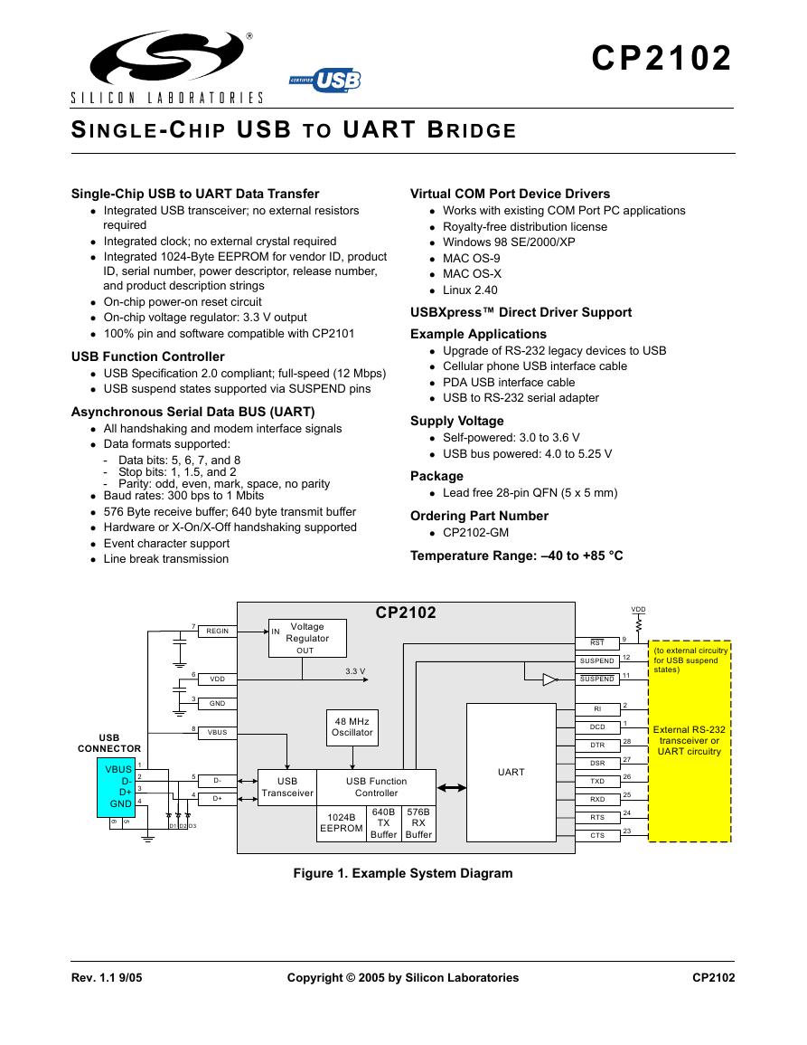
Figure 1. Example System Diagram
Rev. 1.1 9/05
Copyright © 2005 by Silicon Laboratories
CP2102
�
CP2102
2
Rev. 1.1
�
TABLE OF CONTENTS
CP2102
Page
Section
1. System Overview . . . . . . . . . . . . . . . . . . . . . . . . . . . . . . . . . . . . . . . . . . . . . . . . . . . . . . . . .4
2. Absolute Maximum Ratings . . . . . . . . . . . . . . . . . . . . . . . . . . . . . . . . . . . . . . . . . . . . . . . .5
3. Global DC Electrical Characteristics . . . . . . . . . . . . . . . . . . . . . . . . . . . . . . . . . . . . . . . . .5
4. Pinout and Package Definitions . . . . . . . . . . . . . . . . . . . . . . . . . . . . . . . . . . . . . . . . . . . . .6
5. USB Function Controller and Transceiver . . . . . . . . . . . . . . . . . . . . . . . . . . . . . . . . . . . .11
6. Asynchronous Serial Data Bus (UART) Interface . . . . . . . . . . . . . . . . . . . . . . . . . . . . . .12
7. Internal EEPROM . . . . . . . . . . . . . . . . . . . . . . . . . . . . . . . . . . . . . . . . . . . . . . . . . . . . . . . .12
8. Virtual Com Port Device Drivers . . . . . . . . . . . . . . . . . . . . . . . . . . . . . . . . . . . . . . . . . . . .13
9. USBXpress Direct Driver Support . . . . . . . . . . . . . . . . . . . . . . . . . . . . . . . . . . . . . . . . . .13
10. Voltage Regulator . . . . . . . . . . . . . . . . . . . . . . . . . . . . . . . . . . . . . . . . . . . . . . . . . . . . . . .13
Contact Information . . . . . . . . . . . . . . . . . . . . . . . . . . . . . . . . . . . . . . . . . . . . . . . . . . . . . . . .16
Rev. 1.1
3
�
CP2102
1. System Overview
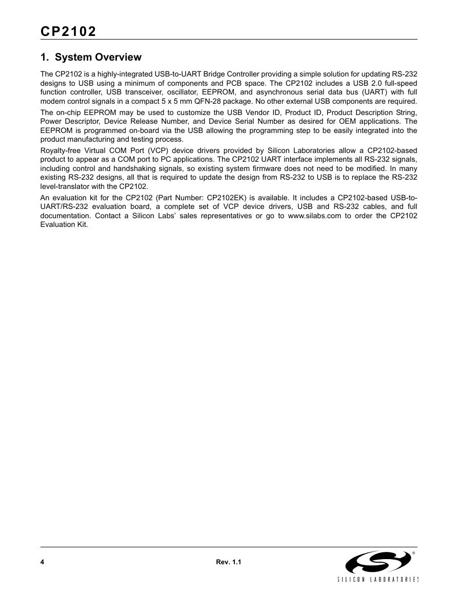
The CP2102 is a highly-integrated USB-to-UART Bridge Controller providing a simple solution for updating RS-232
designs to USB using a minimum of components and PCB space. The CP2102 includes a USB 2.0 full-speed
function controller, USB transceiver, oscillator, EEPROM, and asynchronous serial data bus (UART) with full
modem control signals in a compact 5 x 5 mm QFN-28 package. No other external USB components are required.
The on-chip EEPROM may be used to customize the USB Vendor ID, Product ID, Product Description String,
Power Descriptor, Device Release Number, and Device Serial Number as desired for OEM applications. The
EEPROM is programmed on-board via the USB allowing the programming step to be easily integrated into the
product manufacturing and testing process.
Royalty-free Virtual COM Port (VCP) device drivers provided by Silicon Laboratories allow a CP2102-based
product to appear as a COM port to PC applications. The CP2102 UART interface implements all RS-232 signals,
including control and handshaking signals, so existing system firmware does not need to be modified. In many
existing RS-232 designs, all that is required to update the design from RS-232 to USB is to replace the RS-232
level-translator with the CP2102.
An evaluation kit for the CP2102 (Part Number: CP2102EK) is available. It includes a CP2102-based USB-to-
UART/RS-232 evaluation board, a complete set of VCP device drivers, USB and RS-232 cables, and full
documentation. Contact a Silicon Labs’ sales representatives or go to www.silabs.com to order the CP2102
Evaluation Kit.
4
Rev. 1.1
�
2. Absolute Maximum Ratings
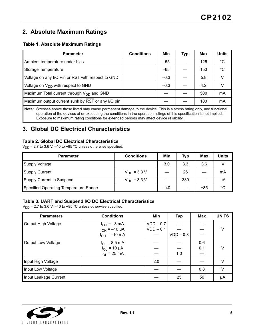
Table 1. Absolute Maximum Ratings
CP2102
Conditions
Parameter
Ambient temperature under bias
Storage Temperature
Voltage on any I/O Pin or RST with respect to GND
Voltage on VDD with respect to GND
Maximum Total current through VDD and GND
Maximum output current sunk by RST or any I/O pin
Note: Stresses above those listed may cause permanent damage to the device. This is a stress rating only, and functional
Units
°C
°C
V
V
mA
mA
Min
–55
–65
–0.3
–0.3
—
—
Typ
—
—
—
—
—
—
Max
125
150
5.8
4.2
500
100
operation of the devices at or exceeding the conditions in the operation listings of this specification is not implied.
Exposure to maximum rating conditions for extended periods may affect device reliability.
3. Global DC Electrical Characteristics
Table 2. Global DC Electrical Characteristics
VDD = 2.7 to 3.6 V, –40 to +85 °C unless otherwise specified.
Parameter
Supply Voltage
Supply Current
Supply Current in Suspend
Specified Operating Temperature Range
Conditions
VDD = 3.3 V
VDD = 3.3 V
Min
3.0
—
—
–40
Typ
3.3
26
330
—
Max
3.6
—
—
+85
Units
V
mA
µA
°C
Table 3. UART and Suspend I/O DC Electrical Characteristics
VDD = 2.7 to 3.6 V, –40 to +85 °C unless otherwise specified.
Parameters
Output High Voltage
Output Low Voltage
Input High Voltage
Input Low Voltage
Input Leakage Current
Conditions
IOH = –3 mA
IOH = –10 µA
IOH = –10 mA
IOL = 8.5 mA
IOL = 10 µA
IOL = 25 mA
Min
VDD – 0.7
VDD – 0.1
—
—
—
—
2.0
—
—
Typ
—
—
VDD – 0.8
—
—
1.0
—
—
25
Max
—
—
—
0.6
0.1
—
—
0.8
50
UNITS
V
V
V
V
µA
Rev. 1.1
5
�
CP2102
4. Pinout and Package Definitions
Name
VDD
GND
RST
REGIN
VBUS
D+
D–
TXD
RXD
CTS
RTS
DSR
DTR
DCD
RI
SUSPEND
SUSPEND
Table 4. CP2102 Pin Definitions
Pin #
Type
Description
6
3
9
7
8
4
5
26
25
23*
24*
27*
28*
1*
2*
12*
11*
Power In
3.0–3.6 V Power Supply Voltage Input.
Power Out
3.3 V Voltage Regulator Output. See
Section 10.
Ground
D I/O
Power In
D In
D I/O
D I/O
Device Reset. Open-drain output of internal POR or VDD monitor.
An external source can initiate a system reset by driving this pin low
for at least 15 µs.
5 V Regulator Input. This pin is the input to the on-chip voltage reg-
ulator.
VBUS Sense Input. This pin should be connected to the VBUS sig-
nal of a USB network. A 5 V signal on this pin indicates a USB net-
work connection.
USB D+
USB D–
D Out
Asynchronous data output (UART Transmit)
D In
D In
Asynchronous data input (UART Receive)
Clear To Send control input (active low)
D Out
Ready to Send control output (active low)
D in
Data Set Ready control input (active low)
D Out
Data Terminal Ready control output (active low)
D In
D In
D Out
D Out
Data Carrier Detect control input (active low)
Ring Indicator control input (active low)
This pin is driven high when the CP2102 enters the USB suspend
state.
This pin is driven low when the CP2102 enters the USB suspend
state.
These pins should be left unconnected or tied to VDD.
NC
10, 13–22
*Note: Pins can be left unconnected when not used.
6
Rev. 1.1
�CP2102
R
T
D
R
S
D
D
X
T
D
X
R
S
T
R
S
T
C
C
N
8
2
7
2
6
2
5
2
4
2
3
2
2
2
21
20
19
18
17
16
15
NC
NC
NC
NC
NC
NC
NC
CP2102
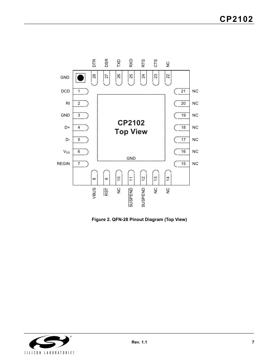
Top View
GND
GND
DCD
RI
GND
D+
D-
VDD
REGIN
1
2
3
4
5
6
7
98
0
1
1
1
2
1
3
1
4
1
S
U
B
V
T
S
R
C
N
C
N
C
N
D
N
E
P
S
U
S
D
N
E
P
S
U
S
Figure 2. QFN-28 Pinout Diagram (Top View)
Rev. 1.1
7
�
CP2102
b
e
L
7
6
5
4
3
2
1
Bottom View
0
8 9 1
1
1
2
1
3
1
4
1
D2
D2
2
2
E
R
2
E
2
DETAIL 1
8
2
7
2
6
2
5
2
4
2
3
2
2
2
6 x e
D
Side View
15
16
17
18
19
20
21
e
x
6
E
A
A1
A2
A3
b
D
D2
E
E2
e
L
N
ND
NE
R
AA
BB
CC
DD
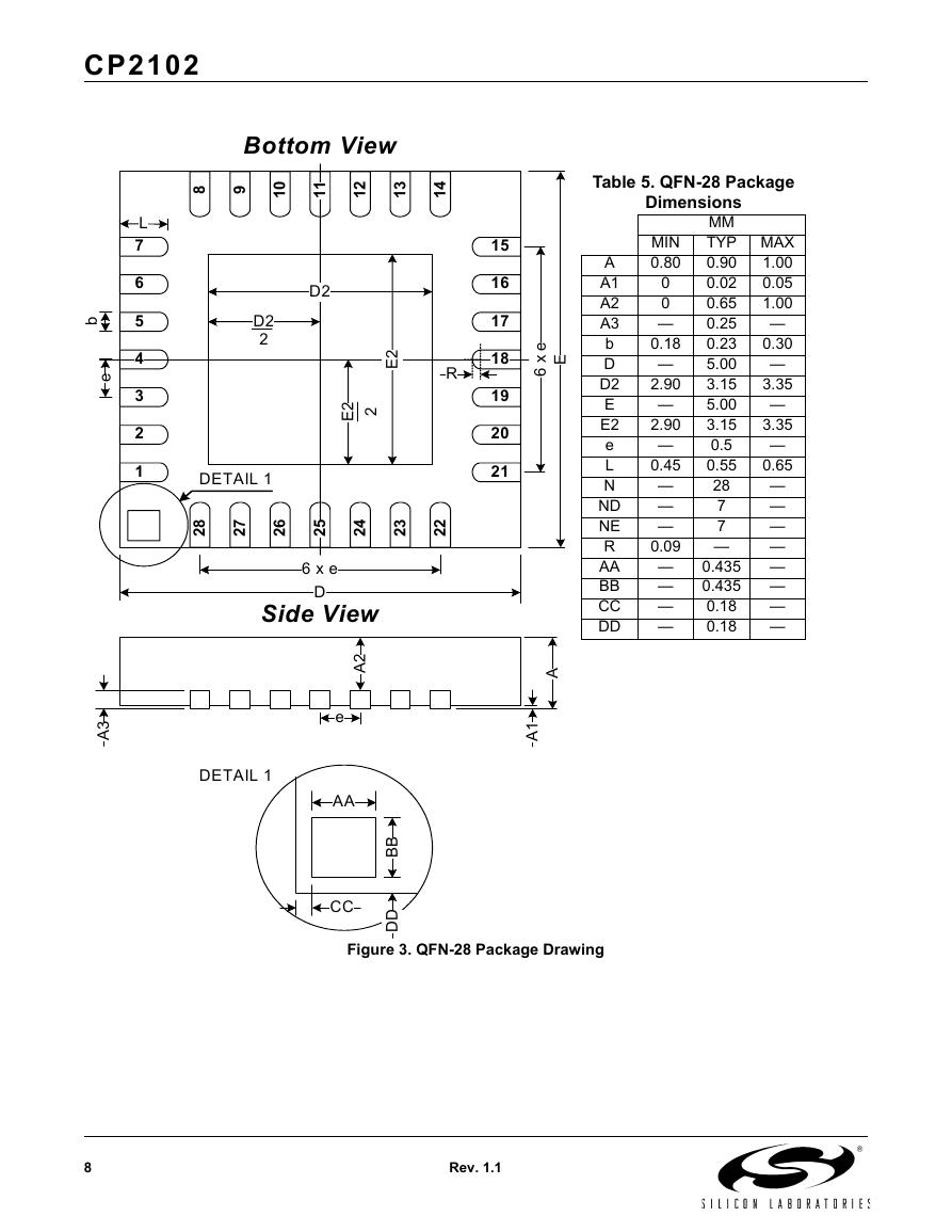
Table 5. QFN-28 Package
MIN
0.80
Dimensions
MM
TYP MAX
1.00
0.90
0.02
0.05
0
1.00
0.65
0
—
0.25
—
0.30
0.23
0.18
5.00
—
—
3.35
3.15
2.90
—
5.00
—
3.35
3.15
2.90
0.5
—
—
0.65
0.55
0.45
—
28
—
7
—
—
—
7
—
0.09
—
—
— 0.435 —
— 0.435 —
—
—
—
—
0.18
0.18
3
A
DETAIL 1
A
1
A
2
A
e
AA
CC
B
B
D
D
Figure 3. QFN-28 Package Drawing
8
Rev. 1.1
�




 V2版本原理图(Capacitive-Fingerprint-Reader-Schematic_V2).pdf
 摄像头工作原理.doc
 VL53L0X简要说明(En.FLVL53L00216).pdf
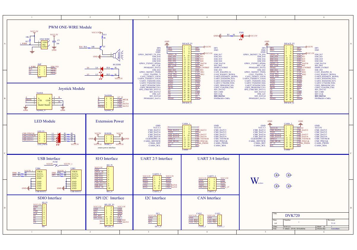 原理图(DVK720-Schematic).pdf
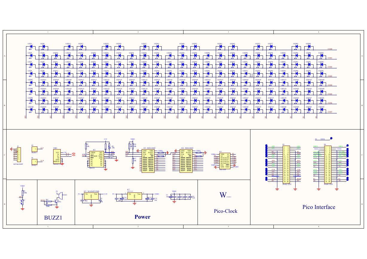 原理图(Pico-Clock-Green-Schdoc).pdf
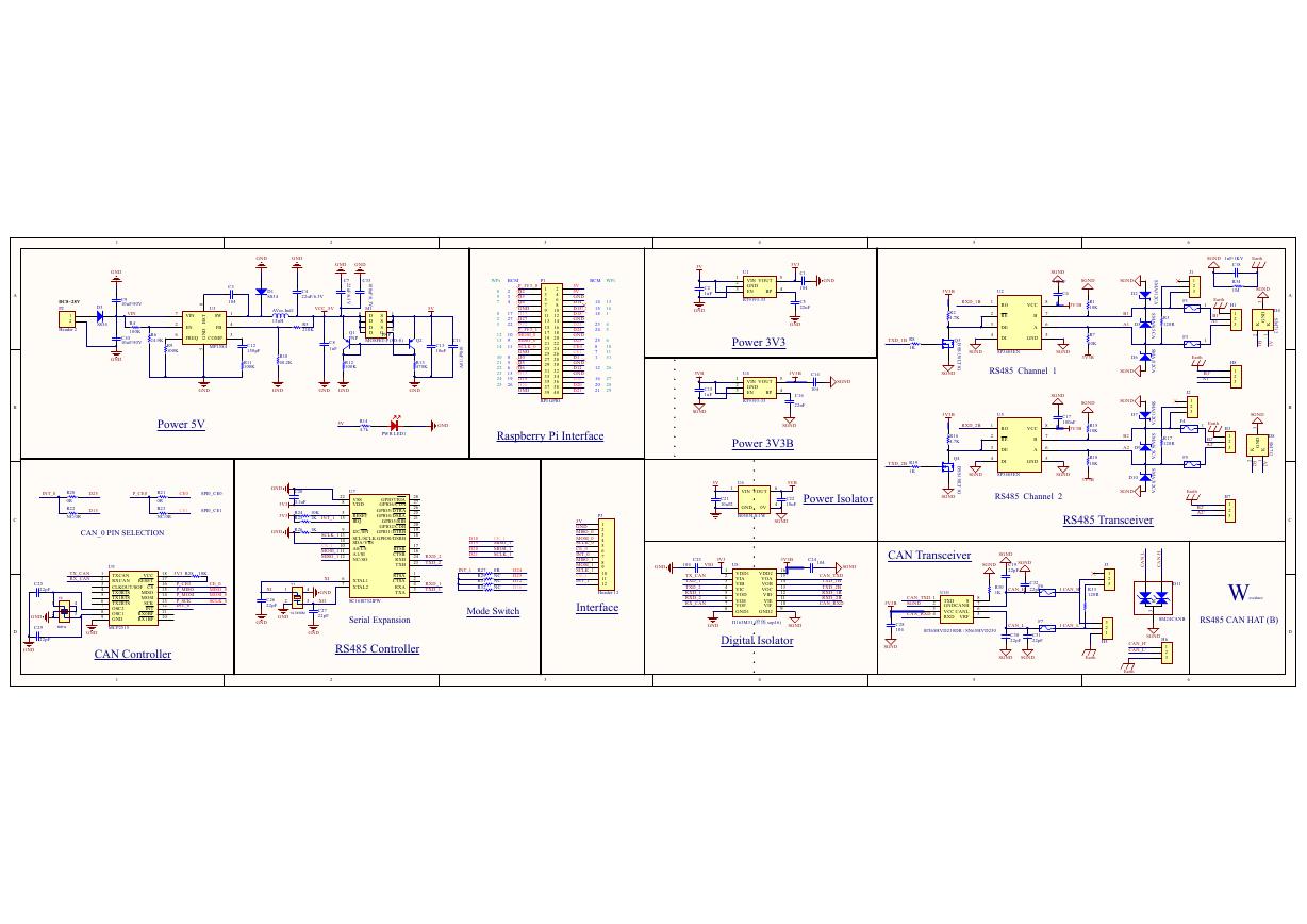 原理图(RS485-CAN-HAT-B-schematic).pdf
 File:SIM7500_SIM7600_SIM7800 Series_SSL_Application Note_V2.00.pdf
 ADS1263(Ads1262).pdf
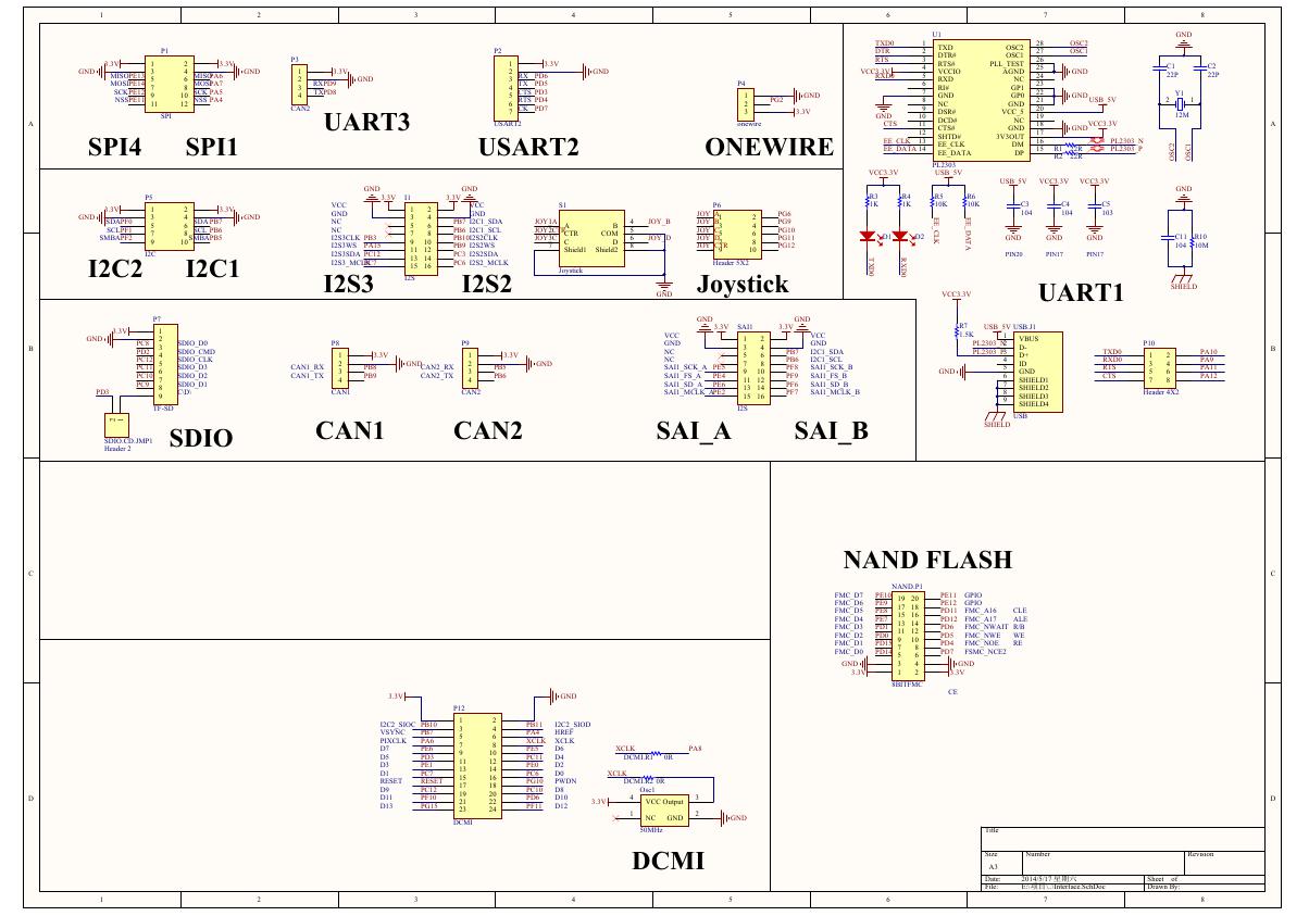 原理图(Open429Z-D-Schematic).pdf
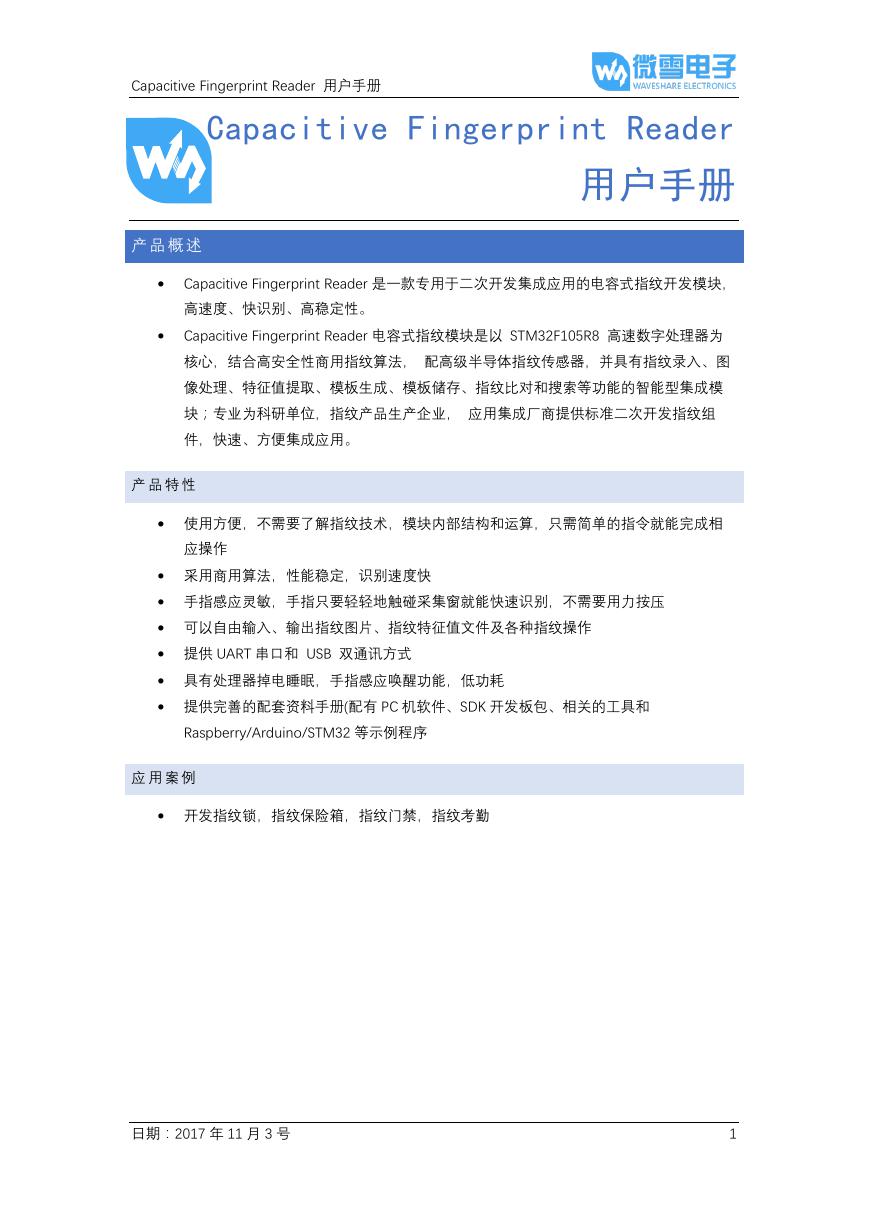 用户手册(Capacitive_Fingerprint_Reader_User_Manual_CN).pdf
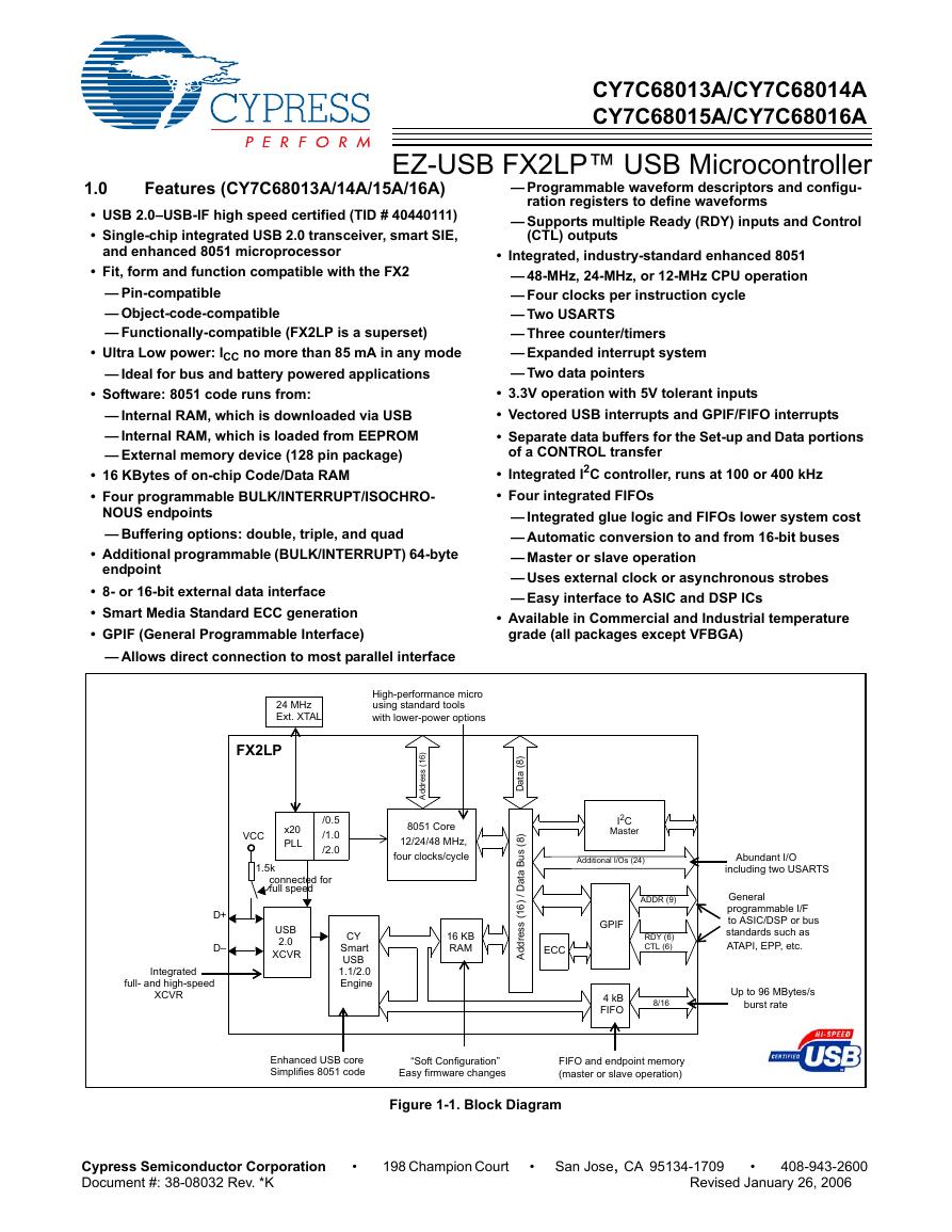 CY7C68013A(英文版)(CY7C68013A).pdf
 TechnicalReference_Dem.pdf