1 Overview
1.1 Technical specification
Table 1. Technical specification
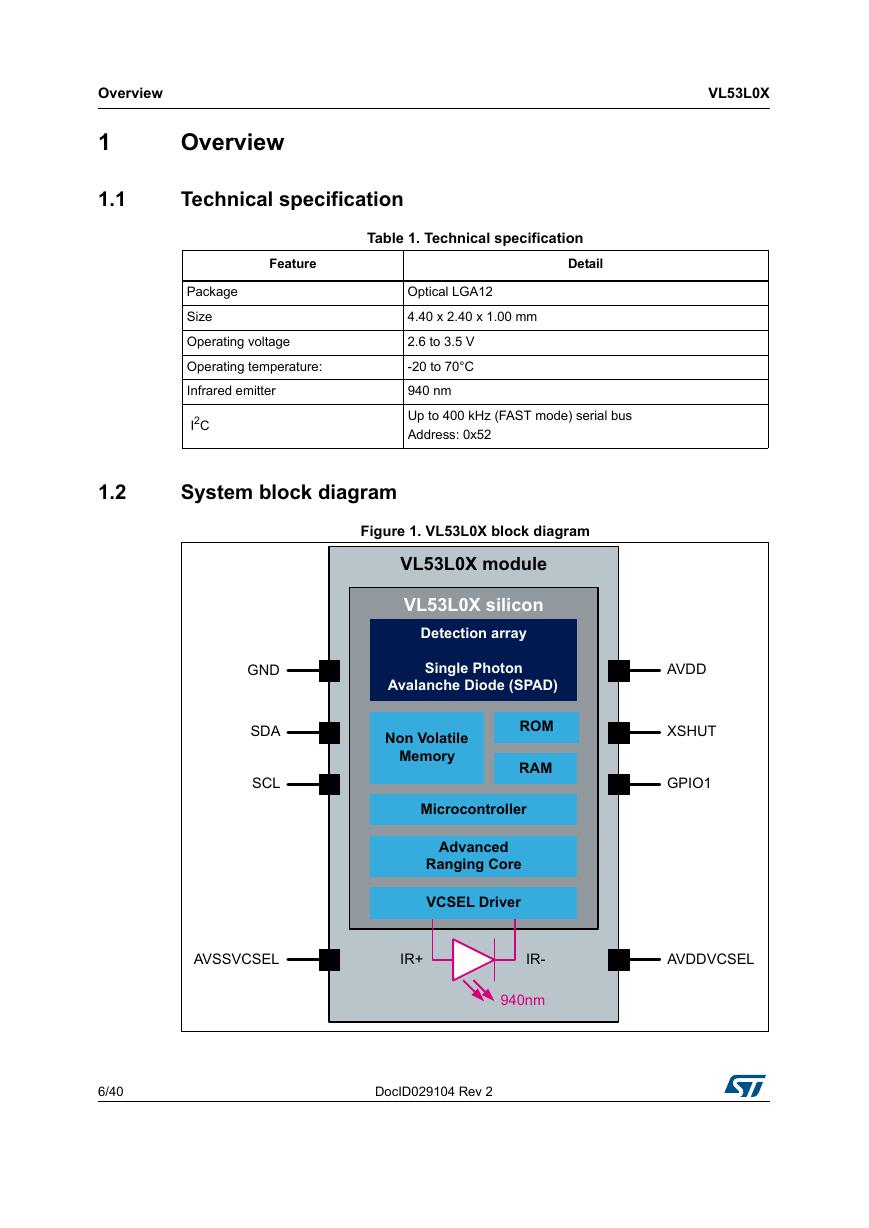
1.2 System block diagram
Figure 1. VL53L0X block diagram
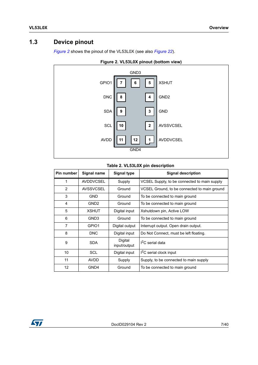
1.3 Device pinout
Figure 2. VL53L0X pinout (bottom view)
Table 2. VL53L0X pin description
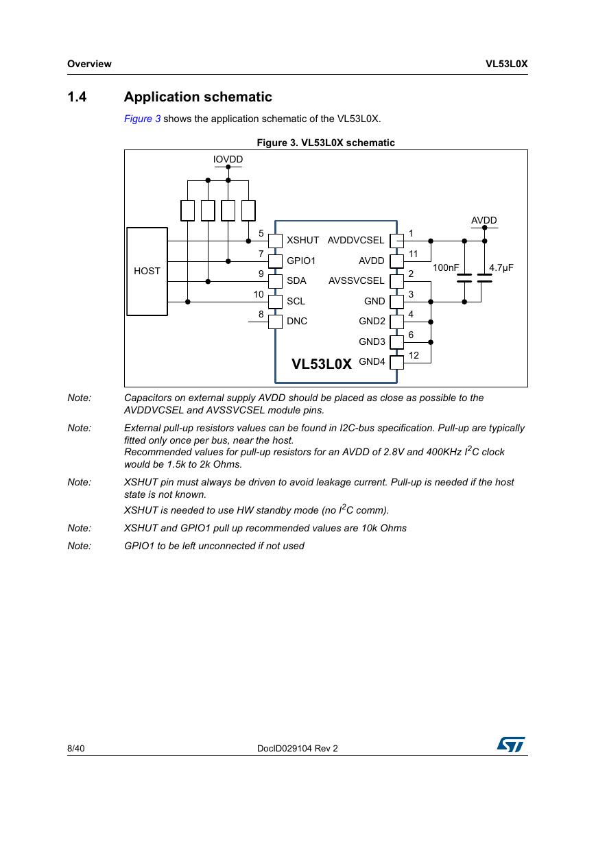
1.4 Application schematic
Figure 3. VL53L0X schematic
2 Functional description
2.1 System functional description
Figure 4. VL53L0X system functional description
2.2 Firmware state machine description
Figure 5. Firmware state machine
2.3 Customer manufacturing calibration flow
Figure 6. Customer manufacturing calibration flow
2.3.1 SPAD and temperature calibration
2.3.2 Ranging offset calibration
Figure 7. Range offset
2.3.3 Cross-talk calibration
Figure 8. Cross-talk compensation
2.4 Ranging operating modes
2.5 Ranging profiles
2.6 Ranging profile phases
Figure 9. Typical initialization / ranging / housekeeping phases
2.6.1 Initialization and load calibration data phase
2.6.2 Ranging phase
2.6.3 Digital housekeeping
2.7 Getting the data: interrupt or polling
2.8 Device programming and control
2.9 Power sequence
2.9.1 Power up and boot sequence
Figure 10. Power up and boot sequence
Figure 11. Power up and boot sequence with XSHUT not controlled
2.10 Ranging sequence
Figure 12. Ranging sequence
3 Control interface
Figure 13. Data transfer protocol
Figure 14. VL53L0X I2C device address: 0x52
Figure 15. VL53L0X data format (write)
Figure 16. VL53L0X data format (read)
Figure 17. VL53L0X data format (sequential write)
Figure 18. VL53L0X data format (sequential read)
3.1 I2C interface - timing characteristics
Table 3. I2C interface - timing characteristics
Figure 19. I2C timing characteristics
3.2 I2C interface - reference registers
Table 4. Reference registers
Table 5. 32-bit register example
4 Electrical characteristics
4.1 Absolute maximum ratings
Table 6. Absolute maximum ratings
4.2 Recommended operating conditions
Table 7. Recommended operating conditions
4.3 ESD
Table 8. ESD performances
4.4 Current consumption
Table 9. Consumption at ambient temperature
4.5 Electrical characteristics
Table 10. Digital I/O electrical characteristics
5 Performance
5.1 Measurement conditions
Figure 20. Typical ranging (default mode)
Figure 21. Typical ranging - long range mode
5.2 Max ranging distance
Table 11. Max ranging capabilities with 33ms timing budget
5.3 Ranging accuracy
5.3.1 Standard deviation
Table 12. Ranging accuracy
5.3.2 Range profile examples
Table 13. Range profiles
5.3.3 Ranging offset error
Table 14. Ranging offset
6 Outline drawing
Figure 22. Outline drawing (page 1/3)
Figure 23. Outline drawing (page 2/3)
Figure 24. Outline drawing - with liner (page 3/3)
7 Laser safety considerations
Figure 25. Class 1 laser product label
8 Packaging and labeling
8.1 Product marking
Figure 26. Example of marking
8.2 Inner box labeling
8.3 Packing
8.3.1 Tape outline drawings
Figure 27. Tape outline drawing
8.4 Pb-free solder reflow process
Table 15. Recommended solder profile
Figure 28. Solder profile
8.5 Handling and storage precautions
8.5.1 Shock precaution
8.5.2 Part handling
8.5.3 Compression force
8.5.4 Moisture sensitivity level
8.6 Storage temperature conditions
Table 16. Recommended storage conditions
9 Ordering information
Table 17. Ordering information
10 Acronyms and abbreviations
Table 18. Acronyms and abbreviations
11 ECOPACK®
12 Revision history
Table 19. Document revision history


 V2版本原理图(Capacitive-Fingerprint-Reader-Schematic_V2).pdf
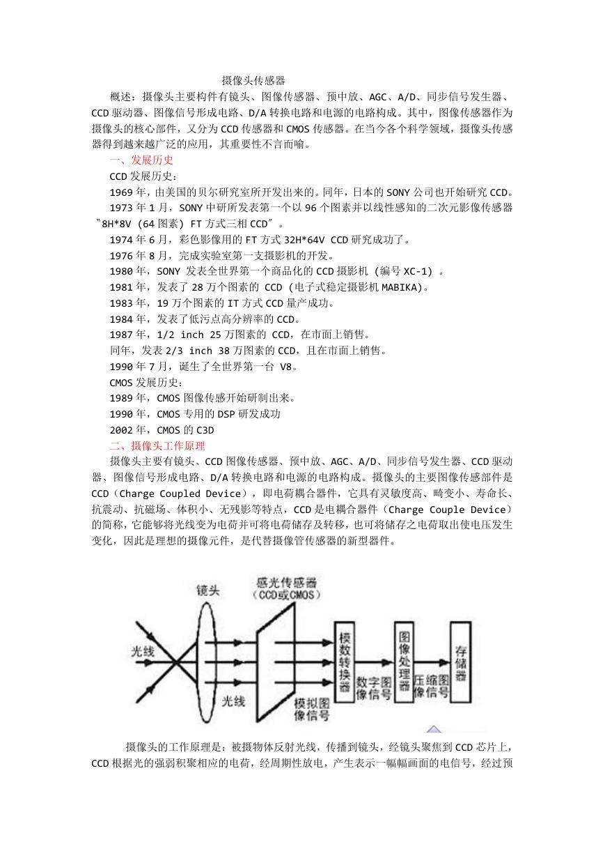 摄像头工作原理.doc
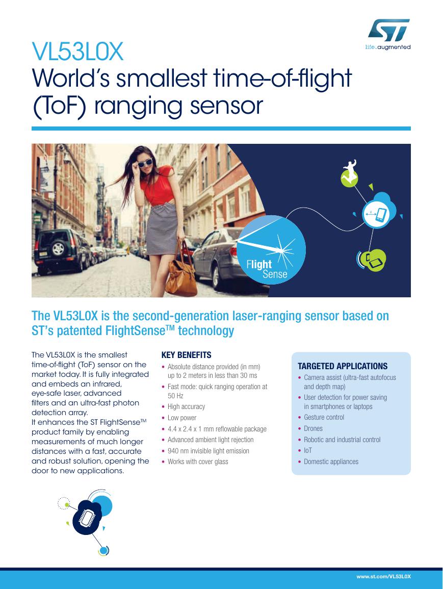 VL53L0X简要说明(En.FLVL53L00216).pdf
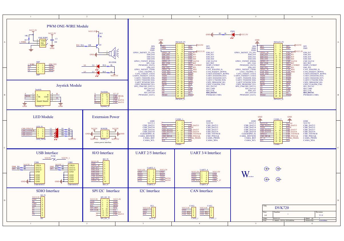 原理图(DVK720-Schematic).pdf
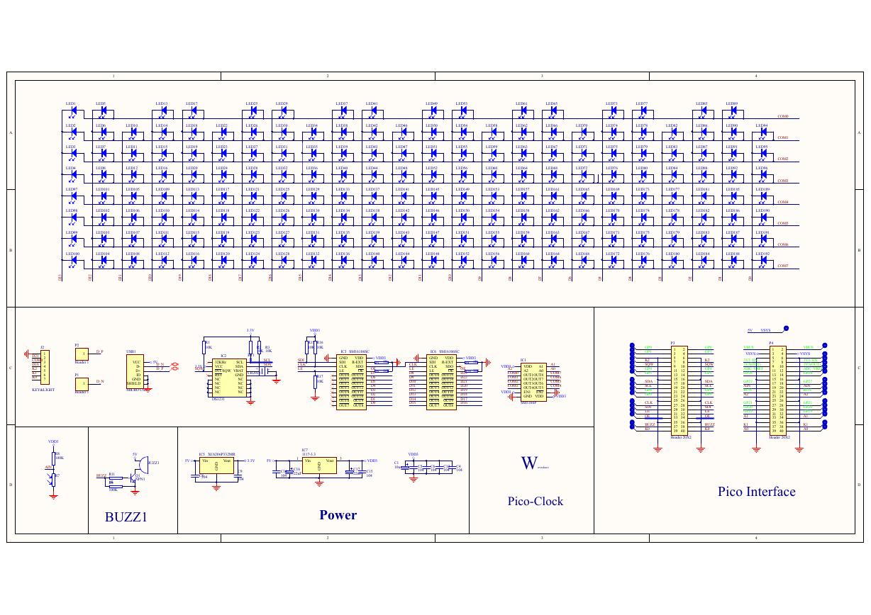 原理图(Pico-Clock-Green-Schdoc).pdf
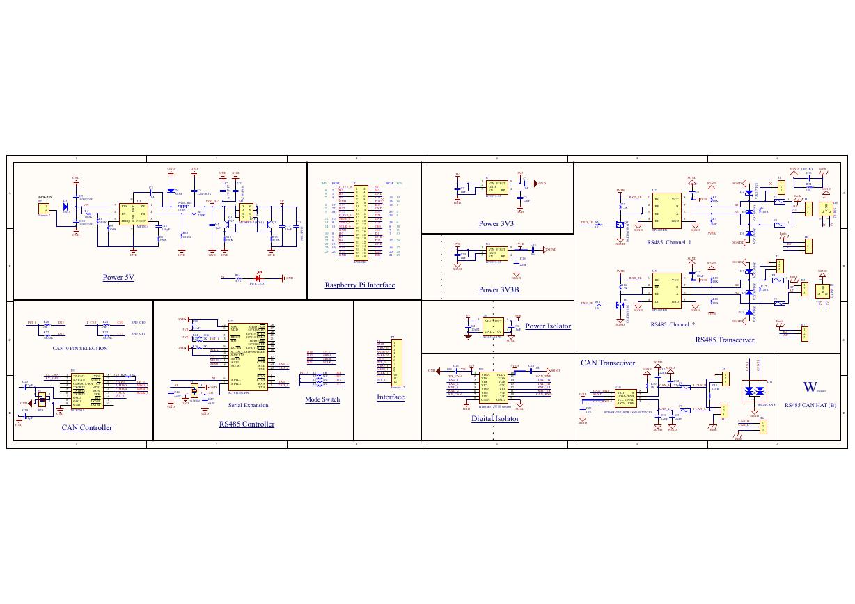 原理图(RS485-CAN-HAT-B-schematic).pdf
 File:SIM7500_SIM7600_SIM7800 Series_SSL_Application Note_V2.00.pdf
 ADS1263(Ads1262).pdf
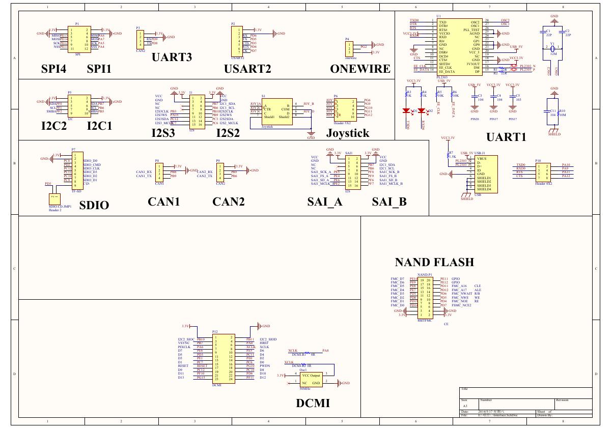 原理图(Open429Z-D-Schematic).pdf
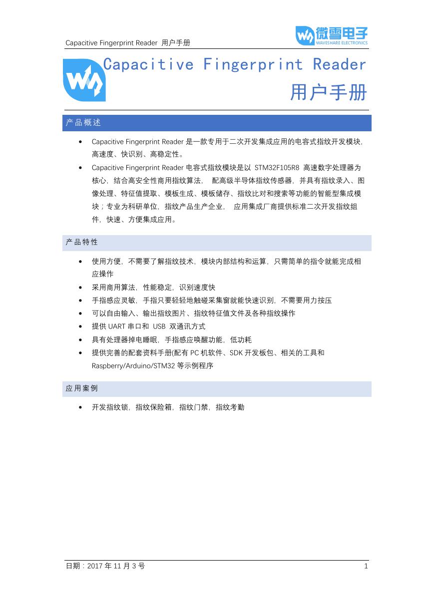 用户手册(Capacitive_Fingerprint_Reader_User_Manual_CN).pdf
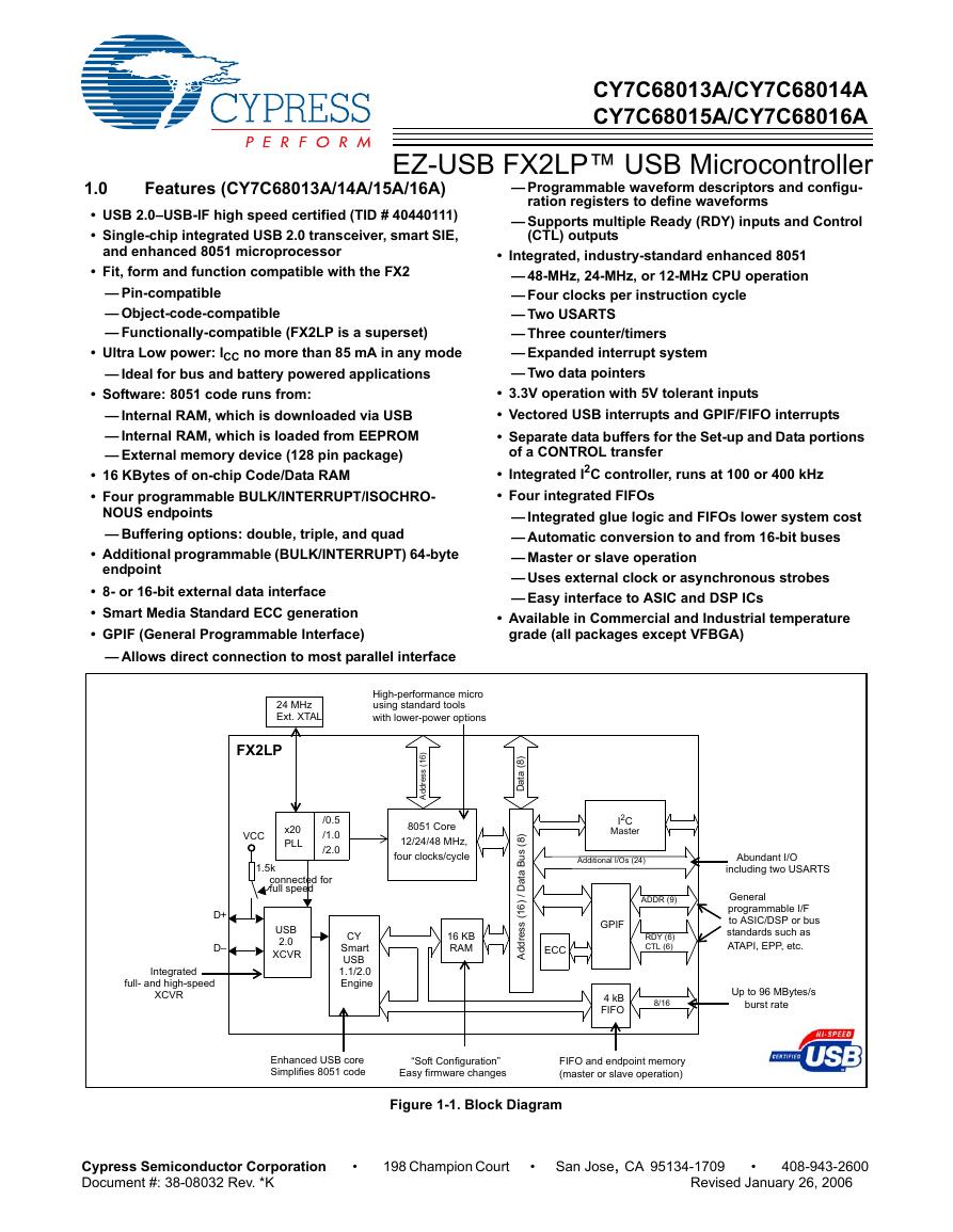 CY7C68013A(英文版)(CY7C68013A).pdf
 TechnicalReference_Dem.pdf