logo资料库

AS7341数据手册 V1.0(AS7341).pdf

第1页 / 共67页
第2页 / 共67页
第3页 / 共67页
第4页 / 共67页
第5页 / 共67页
第6页 / 共67页
第7页 / 共67页
第8页 / 共67页
资料共67页,剩余部分请下载后查看
Content Guide
1 General Description
1.1 Key Benefits & Features
1.2 Applications
1.3 Block Diagram
2 Ordering Information
3 Pin Assignment
3.1 Pin Diagram
3.2 Pin Description
4 Absolute Maximum Ratings
5 Electrical Characteristics
6 Optical Characteristics
7 Typical Operating Characteristics
8 Functional Description
8.1 Channel Architecture
8.2 Sensor Array
8.3 GPIO/INT
8.4 SMUX
8.5 Integration Mode
9 I²C Interface
9.1 I²C Address
9.2 I²C Write Transaction
9.3 I²C Read Transaction
9.4 Timing Characteristics
9.5 Timing Diagrams
10 Register Description
10.1 Register Overview
10.2 Detailed Register Description
10.2.1 Enable and Configuration Register
ENABLE Register (Address 0x80)
CONFIG Register (Address 0x70)
GPIO Register (Address 0x73)
GPIO 2 Register (Address 0xBE)
LED Register (Address 0x74)
INTENAB Register (Address 0xF9)
CONTROL Register (Address 0xFA)
10.2.2 ADC Timing Configuration / Integration Time
ATIME Register (Address 0x81)
ASTEP Register (Address 0xCA, 0xCB)
WTIME Register (Address 0x83)
ITIME Register (Address 0x63, 0x64, 0x65)
EDGE Register (Address 0x72)
FD_TIME Register (Address 0xD8, 0xDA)
10.2.3 ADC Configuration (gain, AGC…)
CFG1 Register (Address 0xAA)
CFG10 Register (Address 0xB3)
AZ_CONFIG Register (Address 0xD6)
AGC_GAIN_MAX Register (Address 0xCF)
CFG8 Register (Address 0xB1)
10.2.4 Device Identification
AUXID Register (Address 0x90)
REVID Register (Address 0x91)
ID Register (Address 0x92)
10.2.5 Spectral Interrupt Configuration
SP_TH_L_LSB Register (Address 0x84)
SP_TH_L_MSB Register (Address 0x85)
SP_TH_H_LSB Register (Address 0x86)
SP _TH_H_MSB Register (Address 0x87)
CFG12 Register (Address 0xB5)
10.2.6 Device Status Register
STAT Register (Address 0x71)
STATUS Register (Address 0x93)
STATUS 2 Register (Address 0xA3)
STATUS 3 Register (Address 0xA4)
STATUS 5 Register (Address 0xA6)
STATUS 6 Register (Address 0xA7)
FD_STATUS Register (Address 0xDB)
10.2.7 Spectral Data and Status
ASTATUS Register (Address 0x60 or 0x94)
CH0_DATA Register (Address 0x95/0x96)
CH1_DATA Register (Address 0x97/0x98)
CH2_DATA Register (Address 0x99/0x9A)
CH3_DATA Register (Address 0x9B/0x9C)
CH4_DATA Register (Address 0x9D/0x9E)
CH5_DATA Register (Address 0x9F/0xA0)
10.2.8 Miscellaneous Configuration
CFG0 Register (Address 0xA9)
CFG3 Register (Address 0xAC)
CFG6 Register (Address 0xAF)
CFG9 Register (Address 0xB2)
PERS Register (Address 0xBD)
10.2.9 FIFO Buffer Data and Status
FIFO_MAP Register (Address 0xFC)
FIFO_CFG0 Register (Address 0xD7)
FIFO_LVL Register (Address 0xFD)
FDATA Register (Address 0xFE and 0xFF)
11 Application Information
11.1 Schematic
11.2 PCB Pad Layout
11.3 Application Optical Requirements
12 Package Drawings & Markings
13 Tape & Reel Information
14 Soldering & Storage Information
14.1 Storage Information
14.1.1 Moisture Sensitivity
14.1.2 Shelf Life
14.1.3 Floor Life
14.1.4 Rebaking Instructions
15 Revision Information
16 Legal Information
Datasheet DS000504 AS7341 11-Channel Spectral Sensor Frontend v1-00 • 2018-Oct-17
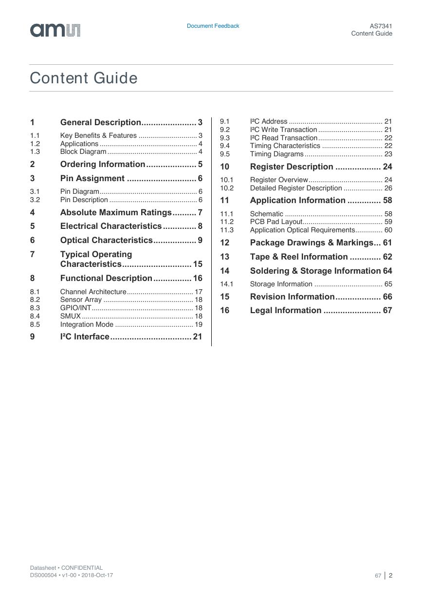
Document Feedback AS7341 Content Guide Content Guide General Description ....................... 3 Key Benefits & Features .............................. 3 Applications .................................................. 4 Block Diagram .............................................. 4 Ordering Information ..................... 5 Pin Assignment ............................. 6 Pin Diagram .................................................. 6 Pin Description ............................................. 6 Absolute Maximum Ratings .......... 7 Electrical Characteristics .............. 8 Optical Characteristics .................. 9 Typical Operating Characteristics ............................. 15 Functional Description ................ 16 Channel Architecture .................................. 17 Sensor Array .............................................. 18 GPIO/INT .................................................... 18 SMUX ......................................................... 18 Integration Mode ........................................ 19 I²C Interface .................................. 21 9.1 9.2 9.3 9.4 9.5 10 10.1 10.2 11 11.1 11.2 11.3 12 13 14 I²C Address ................................................ 21 I²C Write Transaction ................................. 21 I²C Read Transaction ................................. 22 Timing Characteristics ............................... 22 Timing Diagrams ........................................ 23 Register Description ................... 24 Register Overview ...................................... 24 Detailed Register Description .................... 26 Application Information .............. 58 Schematic .................................................. 58 PCB Pad Layout......................................... 59 Application Optical Requirements .............. 60 Package Drawings & Markings ... 61 Tape & Reel Information ............. 62 Soldering & Storage Information 64 14.1 Storage Information ................................... 65 Revision Information ................... 66 Legal Information ........................ 67 15 16 1 1.1 1.2 1.3 2 3 3.1 3.2 4 5 6 7 8 8.1 8.2 8.3 8.4 8.5 9 Datasheet • CONFIDENTIAL DS000504 • v1-00 • 2018-Oct-17 67 │ 2
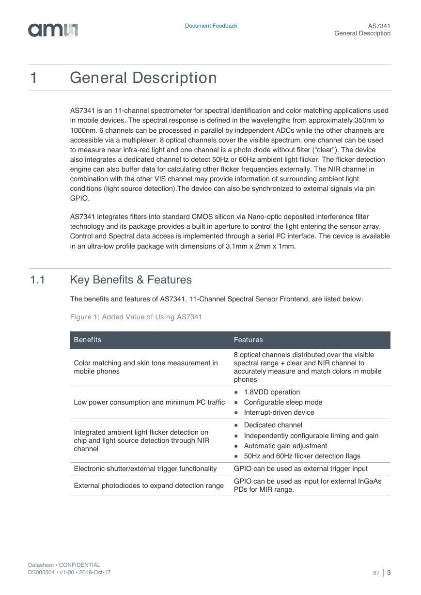
Document Feedback AS7341 General Description 1 General Description AS7341 is an 11-channel spectrometer for spectral identification and color matching applications used in mobile devices. The spectral response is defined in the wavelengths from approximately 350nm to 1000nm. 6 channels can be processed in parallel by independent ADCs while the other channels are accessible via a multiplexer. 8 optical channels cover the visible spectrum, one channel can be used to measure near infra-red light and one channel is a photo diode without filter (“clear”). The device also integrates a dedicated channel to detect 50Hz or 60Hz ambient light flicker. The flicker detection engine can also buffer data for calculating other flicker frequencies externally. The NIR channel in combination with the other VIS channel may provide information of surrounding ambient light conditions (light source detection).The device can also be synchronized to external signals via pin GPIO. AS7341 integrates filters into standard CMOS silicon via Nano-optic deposited interference filter technology and its package provides a built in aperture to control the light entering the sensor array. Control and Spectral data access is implemented through a serial I²C interface. The device is available in an ultra-low profile package with dimensions of 3.1mm x 2mm x 1mm. 1.1 Key Benefits & Features The benefits and features of AS7341, 11-Channel Spectral Sensor Frontend, are listed below: Figure 1: Added Value of Using AS7341 Benefits Features Color matching and skin tone measurement in mobile phones 8 optical channels distributed over the visible spectral range + clear and NIR channel to accurately measure and match colors in mobile phones ● 1.8VDD operation Low power consumption and minimum I²C traffic ● Configurable sleep mode Integrated ambient light flicker detection on chip and light source detection through NIR channel ● Interrupt-driven device ● Dedicated channel ● Independently configurable timing and gain ● Automatic gain adjustment ● 50Hz and 60Hz flicker detection flags Electronic shutter/external trigger functionality GPIO can be used as external trigger input External photodiodes to expand detection range GPIO can be used as input for external InGaAs PDs for MIR range. Datasheet • CONFIDENTIAL DS000504 • v1-00 • 2018-Oct-17 67 │ 3
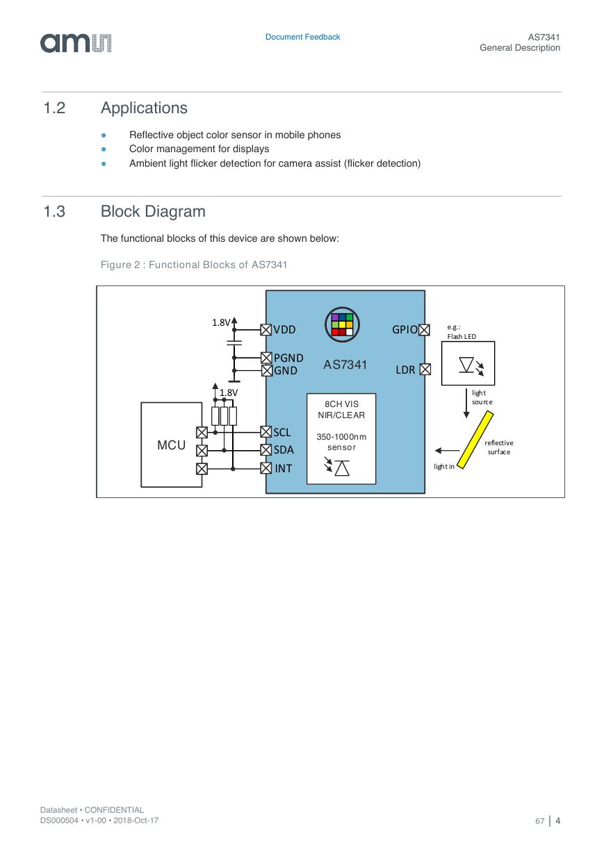
Document Feedback AS7341 General Description 1.2 Applications ● ● ● Reflective object color sensor in mobile phones Color management for displays Ambient light flicker detection for camera assist (flicker detection) 1.3 Block Diagram The functional blocks of this device are shown below: Figure 2 : Functional Blocks of AS7341 67 │ 4 Datasheet • CONFIDENTIAL DS000504 • v1-00 • 2018-Oct-17 AS7341VDDSCLSDA1.8VINTGPIO 8CH VISNIR/CLEAR350-1000nmsensorGNDreflectivesurfacelight inlightsourcee.g.: Flash LEDMCU1.8VLDRPGND
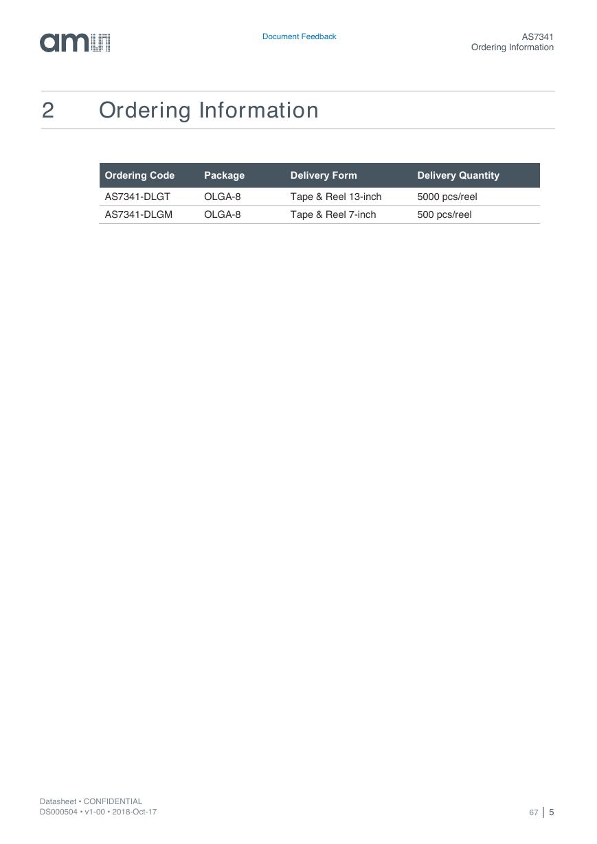
Document Feedback AS7341 Ordering Information 2 Ordering Information Ordering Code Package Delivery Form Delivery Quantity AS7341-DLGT OLGA-8 Tape & Reel 13-inch 5000 pcs/reel AS7341-DLGM OLGA-8 Tape & Reel 7-inch 500 pcs/reel 67 │ 5 Datasheet • CONFIDENTIAL DS000504 • v1-00 • 2018-Oct-17
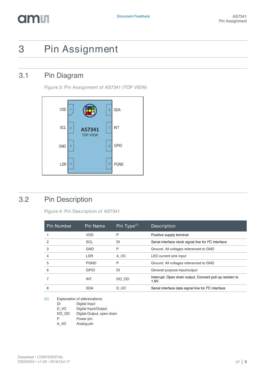
Document Feedback AS7341 Pin Assignment 3 Pin Assignment 3.1 Pin Diagram Figure 3: Pin Assignment of AS7341 (TOP VIEW) 3.2 Pin Description Figure 4: Pin Description of AS7341 Pin Number Pin Name Pin Type(1) Description 1 2 3 4 5 6 7 8 (1) VDD SCL GND LDR PGND GPIO P DI P Positive supply terminal Serial interface clock signal line for I2C interface Ground. All voltages referenced to GND A_I/O LED current sink input P DI Ground. All voltages referenced to GND General purpose input/output INT DO_OD Interrupt. Open drain output. Connect pull up resistor to 1.8V. SDA D_I/O Serial interface data signal line for I2C interface Explanation of abbreviations: DI D_I/O DO_OD P A_I/O Digital Input Digital Input/Output Digital Output, open drain Power pin Analog pin Datasheet • CONFIDENTIAL DS000504 • v1-00 • 2018-Oct-17 67 │ 6 VDDSCLTOP VIEWAS7341INTSDAGPIO23487651GNDLDRPGND
Document Feedback AS7341 Absolute Maximum Ratings 4 Absolute Maximum Ratings Stresses beyond those listed under “Absolute Maximum Ratings“ may cause permanent damage to the device. These are stress ratings only. Functional operation of the device at these or any other conditions beyond those indicated under “Operating Conditions” is not implied. Exposure to absolute maximum rating conditions for extended periods may affect device reliability. All voltages with respect to GND/PGND. Device parameters are guaranteed at VDD=1.8V and TA=25°C unless otherwise noted. Figure 5 Absolute Maximum Ratings of AS7341 Symbol Parameter Min Max Unit Comments Electrical Parameters VDD / VGND Supply Voltage to Ground VANA_MAX Analog Pins VDIG_MAX Digital Pins -0.3 -0.3 -0.3 2.2 3.6 3.6 ISCR IO Input Current (latch-up immunity) ± 100 Output Terminal Current -1 20 Electrostatic Discharge ESDHBM Electrostatic Discharge HBM ± 2000 Temperature Ranges and Storage Conditions TA TSTRG TBODY RHNC Operating Ambient Temperature Storage Temperature Range Package Body Temperature Relative Humidity (non- condensing) -30 -40 5 MSL Moisture Sensitivity Level 85 85 260 85 3 V V V mA mA V °C °C °C % Applicable for pin VDD Applicable for pin LDR Applicable for pins SCL,SDA and INT JEDEC JESD78D Nov 2011 JS-001-2014 IPC/JEDEC J-STD-020(1) Maximum floor life time of 168h (1) The reflow peak soldering temperature (body temperature) is specified according to IPC/JEDEC J-STD-020 “Moisture/Reflow Sensitivity Classification for Nonhermetic Solid State Surface Mount Devices.” The lead finish for Pb- free leaded packages is “Matte Tin” (100% Sn) 67 │ 7 Datasheet • CONFIDENTIAL DS000504 • v1-00 • 2018-Oct-17
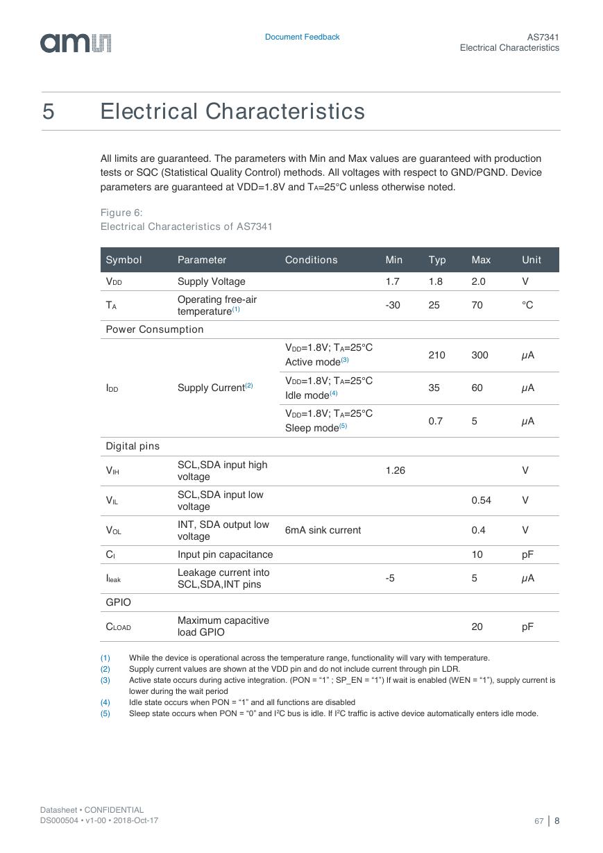
Document Feedback AS7341 Electrical Characteristics 5 Electrical Characteristics All limits are guaranteed. The parameters with Min and Max values are guaranteed with production tests or SQC (Statistical Quality Control) methods. All voltages with respect to GND/PGND. Device parameters are guaranteed at VDD=1.8V and TA=25°C unless otherwise noted. Figure 6: Electrical Characteristics of AS7341 Symbol Parameter Conditions Min Typ Max Unit 1.7 1.8 2.0 -30 25 70 V °C VDD TA Supply Voltage Operating free-air temperature(1) Power Consumption IDD Supply Current(2) Digital pins VIH VIL VOL CI Ileak GPIO CLOAD SCL,SDA input high voltage SCL,SDA input low voltage INT, SDA output low voltage Input pin capacitance Leakage current into SCL,SDA,INT pins Maximum capacitive load GPIO VDD=1.8V; TA=25°C Active mode(3) VDD=1.8V; TA=25°C Idle mode(4) VDD=1.8V; TA=25°C Sleep mode(5) 6mA sink current 1.26 -5 210 300 µA 35 60 µA 0.7 5 µA 0.54 0.4 10 5 20 V V V pF µA pF (1) (2) (3) (4) (5) While the device is operational across the temperature range, functionality will vary with temperature. Supply current values are shown at the VDD pin and do not include current through pin LDR. Active state occurs during active integration. (PON = “1” ; SP_EN = “1”) If wait is enabled (WEN = “1”), supply current is lower during the wait period Idle state occurs when PON = “1” and all functions are disabled Sleep state occurs when PON = “0” and I2C bus is idle. If I2C traffic is active device automatically enters idle mode. Datasheet • CONFIDENTIAL DS000504 • v1-00 • 2018-Oct-17 67 │ 8
分享到:
收藏