SIM868_RF_Design_Application
Note_V1.00
SIMCOM CONFIDENTIAL FILE�
Smart Machine Smart Decision
Document Title:
SIM868_RF_Design_Application Note_V1.00
Version:
Date:
Status:
V1.00
2016-09-13
Released
SIM868_RF Design Guide_V1.00
Document Control ID:
General Notes
SIMCom offers this information as a service to its customers, to support application and engineering efforts that
use the products designed by SIMCom. The information provided is based upon requirements specifically
provided to SIMCom by the customers. SIMCom has not undertaken any independent search for additional
relevant information, including any information that may be in the customer’s possession. Furthermore, system
validation of this product designed by SIMCom within a larger electronic system remains the responsibility of the
customer or the customer’s system integrator. All specifications supplied herein are subject to change.
Copyright
This document contains proprietary technical information which is the property of SIMCom Limited., copying of
this document and giving it to others and the using or communication of the contents thereof, are forbidden
without express authority. Offenders are liable to the payment of damages. All rights reserved in the event of grant
of a patent or the registration of a utility model or design. All specification supplied herein are subject to change
without notice at any time.
Copyright © Shanghai SIMCom Wireless Solutions Ltd. 2008
SIM868_RF_Design_Application Note_V1.00 2016-09-13
2
SIMCOM CONFIDENTIAL FILE�
Smart Machine Smart Decision
Contents
Contents ..................................................................................................................................................................... 3
Version history .......................................................................................................................................................... 4
1
Introduction ......................................................................................................................................................... 5
2 SIM868 RF Interface overview .......................................................................................................................... 5
3 Circuit Design ..................................................................................................................................................... 5
3.1 GSM antenna interface ................................................................................................................................. 5
3.2 BT antenna interface ..................................................................................................................................... 7
3.3 GNSS antenna interface................................................................................................................................ 7
3.4 Power supply circuit design .......................................................................................................................... 8
3.5 Noise Suppression Consideration ................................................................................................................. 9
4 Components placement and PCB layout ............................................................................................................11
4.1 Antenna part ................................................................................................................................................11
4.2 Two-layer PCB RF trace design .................................................................................................................. 12
4.2.1 1.0mm Two-layer PCB ...................................................................................................................... 12
4.2.2 1.6mm Two-layer PCB ...................................................................................................................... 13
4.3 Power supply part ....................................................................................................................................... 14
SIM868_RF_Design_Application Note_V1.00 2016-09-13
3
SIMCOM CONFIDENTIAL FILE�
Smart Machine Smart Decision
Version history
Version Description of change
1.00
Initial version
Date
2016-09-13
Author
Chen Xiaoxu
SIM868_RF_Design_Application Note_V1.00 2016-09-13
4
SIMCOM CONFIDENTIAL FILE�
Smart Machine Smart Decision
1 Introduction
This document describes the SIM868 module RF antenna interface and recommended antenna
performance specifications. In order to get better RF performance, the customer should follow
antenna design guides in the document.
2 SIM868 RF Interface overview
Designed for global market, SIM868 is integrated with a high performance GSM/GPRS engine , a
BT engine and a GNSS engine.
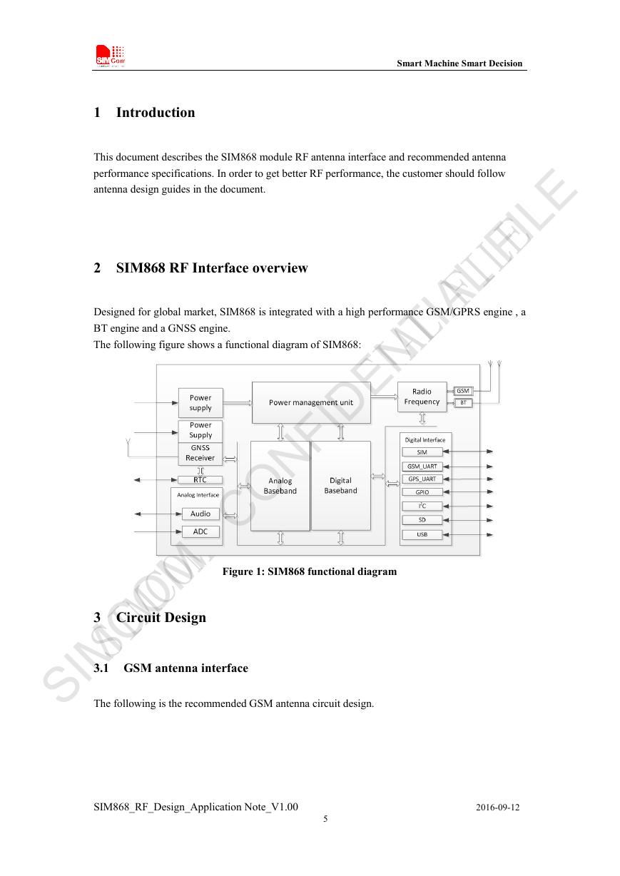
The following figure shows a functional diagram of SIM868:
Figure 1: SIM868 functional diagram
3 Circuit Design
3.1 GSM antenna interface
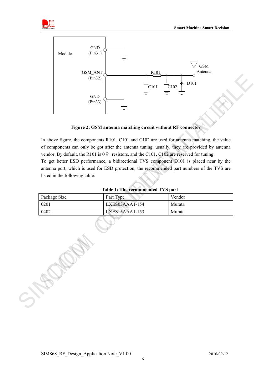
The following is the recommended GSM antenna circuit design.
SIM868_RF_Design_Application Note_V1.00 2016-09-12
5
SIMCOM CONFIDENTIAL FILE�
Smart Machine Smart Decision
Module
GND
(Pin31)
GSM_ANT
(Pin32)
GND
(Pin33)
R101
GSM
Antenna
C101
C102
D101
Figure 2: GSM antenna matching circuit without RF connector
In above figure, the components R101, C101 and C102 are used for antenna matching, the value
of components can only be got after the antenna tuning, usually, they are provided by antenna
vendor. By default, the R101 is 0Ω resistors, and the C101, C102 are reserved for tuning.
To get better ESD performance, a bidirectional TVS component D101 is placed near by the
antenna port, which is used for ESD protection, the recommended part numbers of the TVS are
listed in the following table:
Table 1: The recommended TVS part
Part Type
LXES03AAA1-154
LXES15AAA1-153
Vendor
Murata
Murata
Package Size
0201
0402
SIM868_RF_Design_Application Note_V1.00 2016-09-12
6
SIMCOM CONFIDENTIAL FILE�
Smart Machine Smart Decision
3.2 BT antenna interface
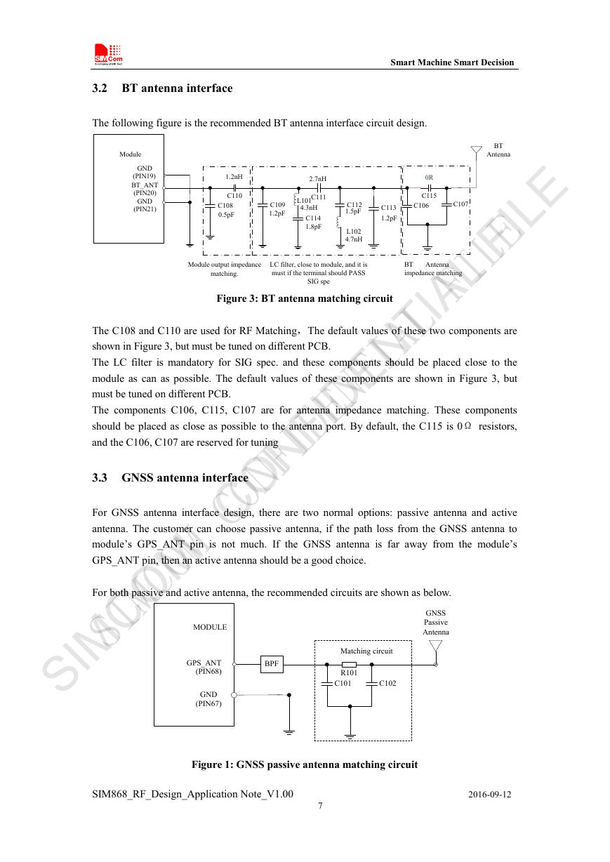
The following figure is the recommended BT antenna interface circuit design.
Module
GND
(PIN19)
BT_ANT
(PIN20)
GND
(PIN21)
1.2nH
C110
C108
0.5pF
2.7nH
C111
L101
4.3nH
C114
1.8pF
C109
1.2pF
C113
1.2pF
C112
1.5pF
L102
4.7nH
BT
Antenna
0R
C115
C106
C107
Module output impedance
matching.
LC filter, close to module, and it is
must if the terminal should PASS
SIG spe
BT Antenna
impedance matching
Figure 3: BT antenna matching circuit
The C108 and C110 are used for RF Matching,The default values of these two components are
shown in Figure 3, but must be tuned on different PCB.
The LC filter is mandatory for SIG spec. and these components should be placed close to the
module as can as possible. The default values of these components are shown in Figure 3, but
must be tuned on different PCB.
The components C106, C115, C107 are for antenna impedance matching. These components
should be placed as close as possible to the antenna port. By default, the C115 is 0Ω resistors,
and the C106, C107 are reserved for tuning
3.3 GNSS antenna interface
For GNSS antenna interface design, there are two normal options: passive antenna and active
antenna. The customer can choose passive antenna, if the path loss from the GNSS antenna to
module’s GPS_ANT pin is not much. If the GNSS antenna is far away from the module’s
GPS_ANT pin, then an active antenna should be a good choice.
For both passive and active antenna, the recommended circuits are shown as below.
MODULE
GPS_ANT
(PIN68)
GND
(PIN67)
BPF
Matching circuit
R101
C101
C102
GNSS
Passive
Antenna
Figure 1: GNSS passive antenna matching circuit
SIM868_RF_Design_Application Note_V1.00 2016-09-12
7
SIMCOM CONFIDENTIAL FILE�
Smart Machine Smart Decision
MODULE
VCC_ANT
R102 10Ω
L101
27nH
BPF
GPS_ANT
(PIN68)
GND
(PIN67)
Matching circuit
R101
C101
C102
GNSS
Active
Antenna
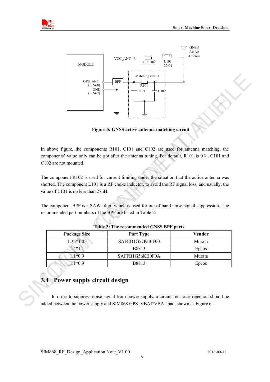
Figure 5: GNSS active antenna matching circuit
In above figure, the components R101, C101 and C102 are used for antenna matching, the
components’ value only can be got after the antenna tuning. For default, R101 is 0Ω, C101 and
C102 are not mounted.
The component R102 is used for current limiting under the situation that the active antenna was
shorted. The component L101 is a RF choke inductor, to avoid the RF signal loss, and usually, the
value of L101 is no less than 27nH.
The component BPF is a SAW filter, which is used for out of band noise signal suppression. The
recommended part numbers of the BPF are listed in Table 2:
Table 2: The recommended GNSS BPF parts
Package Size
1.35*1.05
1.4*1.1
1.1*0.9
1.1*0.9
Part Type
SAFEB1G57KE0F00
B8313
SAFFB1G56KB0F0A
B8813
Vendor
Murata
Epcos
Murata
Epcos
3.4 Power supply circuit design
In order to suppress noise signal from power supply, a circuit for noise rejection should be
added between the power supply and SIM868 GPS_VBAT/VBAT pad, shown as Figure 6.
SIM868_RF_Design_Application Note_V1.00 2016-09-12
8
SIMCOM CONFIDENTIAL FILE�



 V2版本原理图(Capacitive-Fingerprint-Reader-Schematic_V2).pdf
 摄像头工作原理.doc
 VL53L0X简要说明(En.FLVL53L00216).pdf
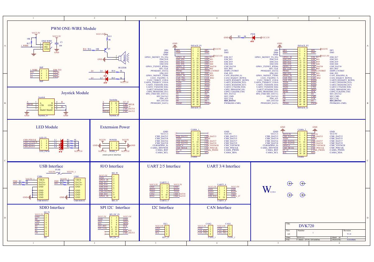 原理图(DVK720-Schematic).pdf
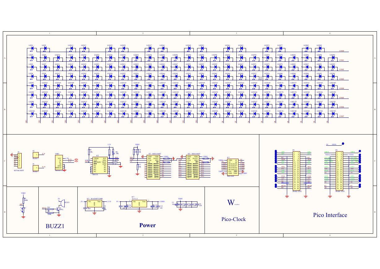 原理图(Pico-Clock-Green-Schdoc).pdf
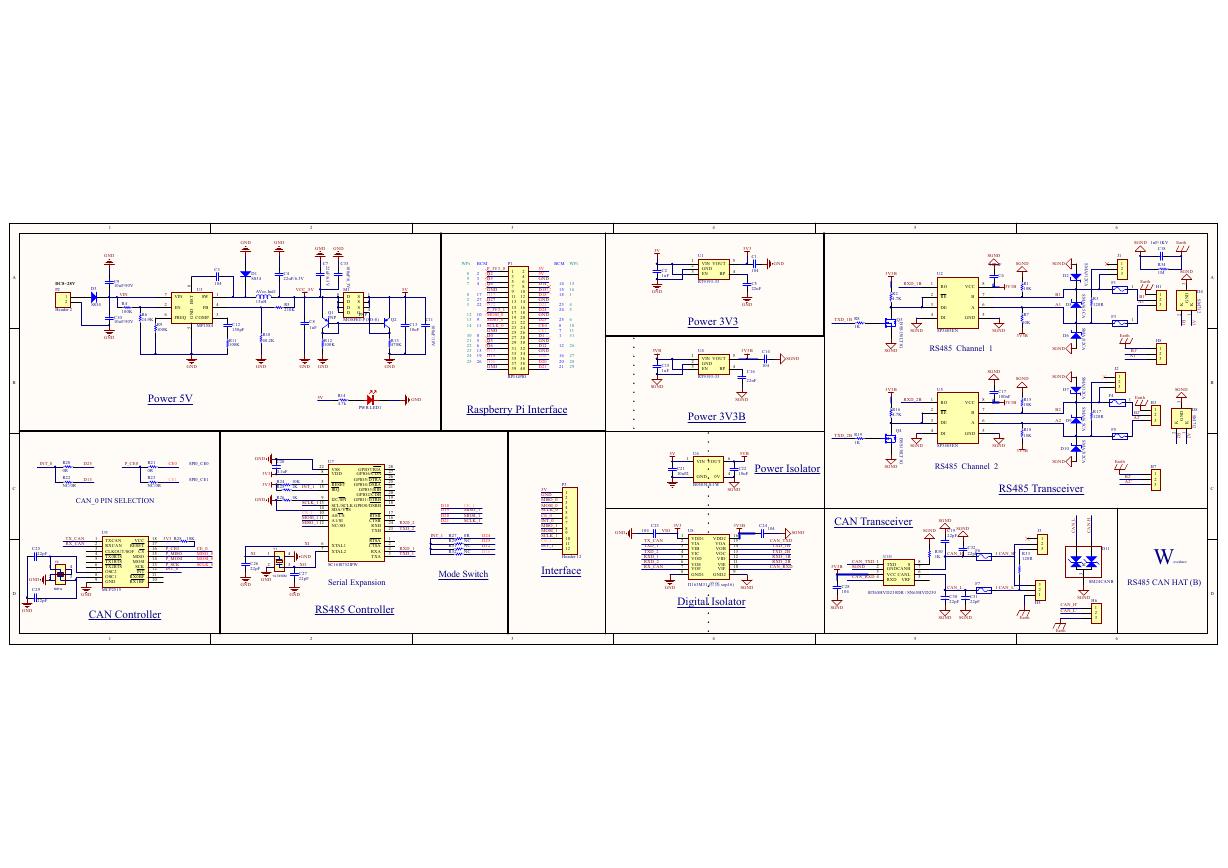 原理图(RS485-CAN-HAT-B-schematic).pdf
 File:SIM7500_SIM7600_SIM7800 Series_SSL_Application Note_V2.00.pdf
 ADS1263(Ads1262).pdf
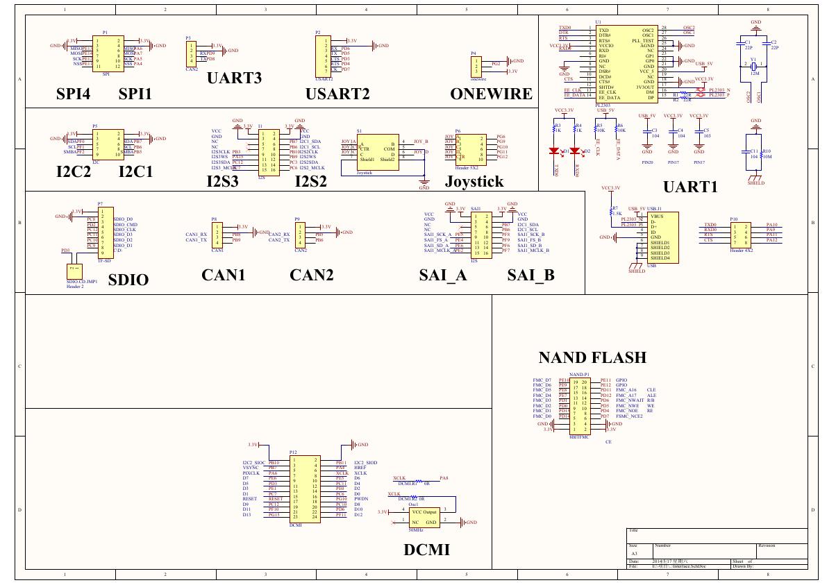 原理图(Open429Z-D-Schematic).pdf
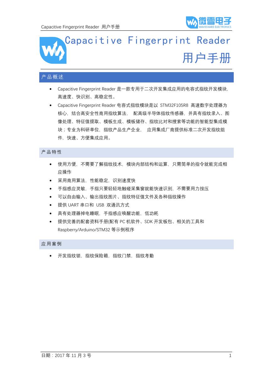 用户手册(Capacitive_Fingerprint_Reader_User_Manual_CN).pdf
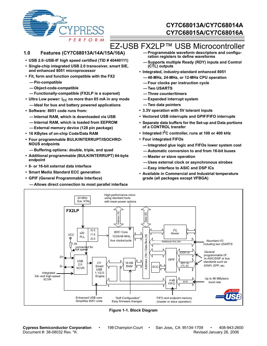 CY7C68013A(英文版)(CY7C68013A).pdf
 TechnicalReference_Dem.pdf