DAC8532
SBAS246A – DECEMBER 2001 – MAY 2003
Dual Channel, Low Power, 16-Bit, Serial Input
DIGITAL-TO-ANALOG CONVERTER
FEATURES
G microPOWER OPERATION: 500µA at 5V
G POWER-ON RESET TO ZERO-SCALE
G POWER SUPPLY: +2.7V to +5.5V
G 16-BIT MONOTONIC OVER TEMPERATURE
G SETTLING TIME: 10µs to ±0.003% FSR
G ULTRA-LOW AC CROSSTALK: –100dB typ
G LOW-POWER SERIAL INTERFACE WITH
SCHMITT-TRIGGERED INPUTS
G ON-CHIP OUTPUT BUFFER AMPLIFIER WITH
RAIL-TO-RAIL OPERATION
G DOUBLE BUFFERED INPUT ARCHITECTURE
G SIMULTANEOUS OR SEQUENTIAL OUTPUT
UPDATE AND POWERDOWN
G TINY MSOP-8 PACKAGE
APPLICATIONS
G PORTABLE INSTRUMENTATION
G CLOSED-LOOP SERVO-CONTROL
G PROCESS CONTROL
G DATA ACQUISITION SYSTEMS
G PROGRAMMABLE ATTENUATION
G PC PERIPHERALS
DESCRIPTION
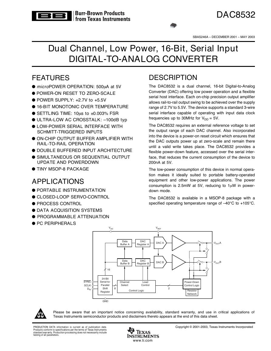
The DAC8532 is a dual channel, 16-bit Digital-to-Analog
Converter (DAC) offering low power operation and a flexible
serial host interface. Each on-chip precision output amplifier
allows rail-to-rail output swing to be achieved over the supply
range of 2.7V to 5.5V. The device supports a standard 3-wire
serial interface capable of operating with input data clock
frequencies up to 30MHz for VDD = 5V.
The DAC8532 requires an external reference voltage to set
the output range of each DAC channel. Also incorporated
into the device is a power-on reset circuit which ensures that
the DAC outputs power up at zero-scale and remain there
until a valid write takes place. The DAC8532 provides a
flexible power-down feature, accessed over the serial inter-
face, that reduces the current consumption of the device to
200nA at 5V.
The low-power consumption of this device in normal opera-
tion makes it ideally suited to portable battery-operated
equipment and other low-power applications. The power
consumption is 2.5mW at 5V, reducing to 1µW in power-
down mode.
The DAC8532 is available in a MSOP-8 package with a
specified operating temperature range of –40°C to +105°C.
VDD
VREF
Data
Buffer A
DAC
Register A
DAC A
Data
Buffer B
DAC
Register B
DAC B
VOUTA
VOUTB
SYNC
SCLK
DIN
16
24-Bit
Serial-to-
Parallel
Shift
Register
8
GND
Channel
Select
Load
Control
Control Logic
2
Power-Down
Control Logic
Resistor
Network
Please be aware that an important notice concerning availability, standard warranty, and use in critical applications of
Texas Instruments semiconductor products and disclaimers thereto appears at the end of this data sheet.
PRODUCTION DATA information is current as of publication date.
Products conform to specifications per the terms of Texas Instruments
standard warranty. Production processing does not necessarily include
testing of all parameters.
www.ti.com
Copyright © 2001-2003, Texas Instruments Incorporated
�
ABSOLUTE MAXIMUM RATINGS(1)
VDD to GND ........................................................................... –0.3V to +6V
Digital Input Voltage to GND ................................. –0.3V to +VDD + 0.3V
VOUTA or VOUTB to GND .......................................... –0.3V to +VDD + 0.3V
Operating Temperature Range ...................................... –40°C to +105°C
Storage Temperature Range ......................................... –65°C to +150°C
Junction Temperature Range (TJ max) ........................................ +150°C
Power Dissipation ........................................................ (TJ max — TA)/θJA
θJA Thermal Impedance ......................................................... 206°C/W
θJC Thermal Impedance .......................................................... 44°C/W
Lead Temperature, Soldering:
Vapor Phase (60s) ............................................................... +215°C
Infrared (15s) ........................................................................ +220°C
NOTE: (1) Stresses above those listed under “Absolute Maximum Ratings”
may cause permanent damage to the device. Exposure to absolute maximum
conditions for extended periods may affect device reliability.
ELECTROSTATIC
DISCHARGE SENSITIVITY
This integrated circuit can be damaged by ESD. Texas Instru-
ments recommends that all integrated circuits be handled with
appropriate precautions. Failure to observe proper handling
and installation procedures can cause damage.
ESD damage can range from subtle performance degradation
to complete device failure. Precision integrated circuits may be
more susceptible to damage because very small parametric
changes could cause the device not to meet its published
specifications.
PACKAGE/ORDERING INFORMATION
PRODUCT
PACKAGE-LEAD
PACKAGE
DESIGNATOR(1)
DAC8532
MSOP-8
"
DGK
"
SPECIFICATION
TEMPERATURE
RANGE
–40°C to +105°C
"
PACKAGE
MARKING
ORDERING
NUMBER
TRANSPORT
MEDIA, QUANTITY
D32E
"
DAC8532IDGK
DAC8532IDGKR
Tube, 80
Tape and Reel,
2500
NOTE: (1) For the most current specifications and package information, refer to our web site at www.ti.com.
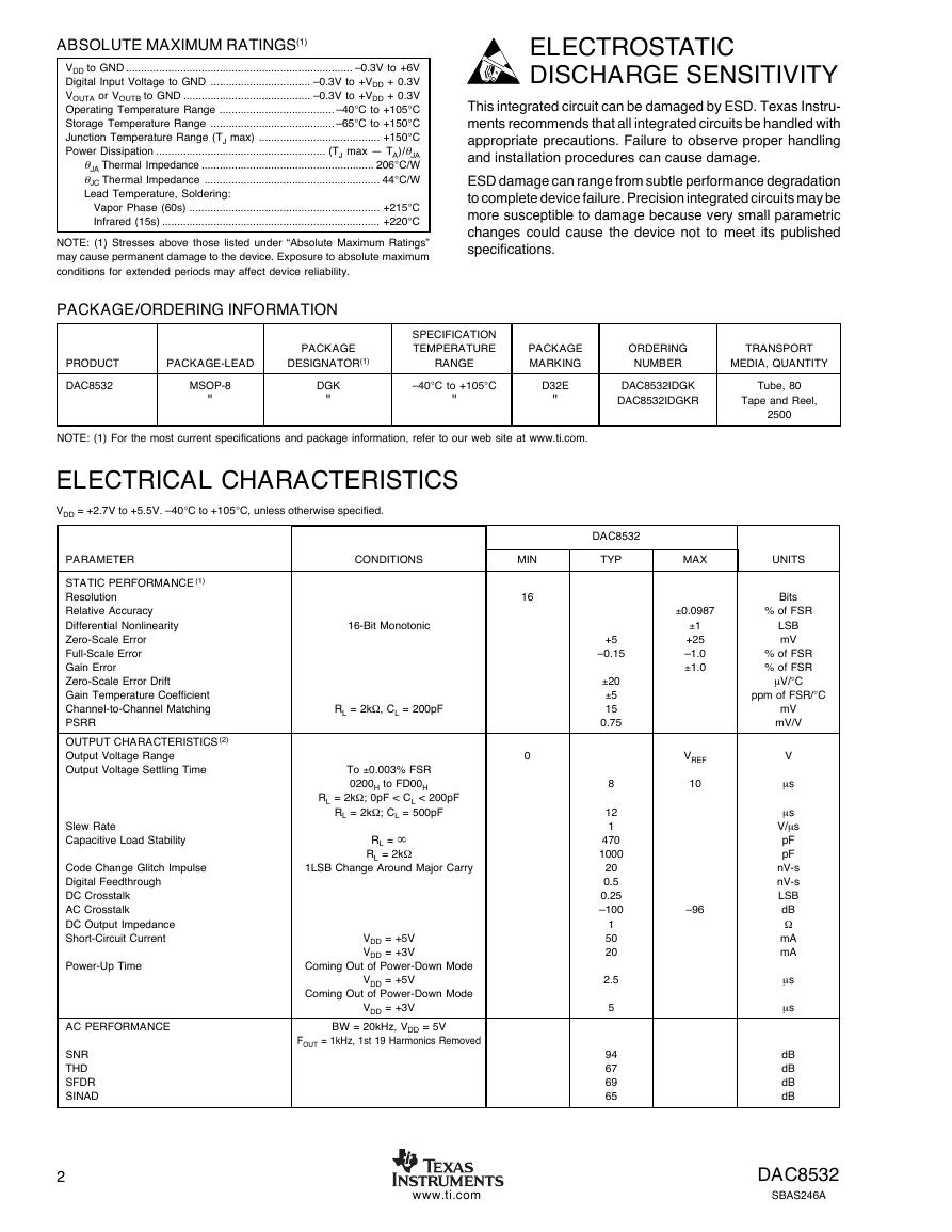
ELECTRICAL CHARACTERISTICS
VDD = +2.7V to +5.5V. –40°C to +105°C, unless otherwise specified.
PARAMETER
CONDITIONS
16-Bit Monotonic
RL = 2kΩ, CL = 200pF
To ±0.003% FSR
0200H to FD00H
RL = 2kΩ; 0pF < CL < 200pF
RL = 2kΩ; CL = 500pF
RL = ∞
RL = 2kΩ
1LSB Change Around Major Carry
VDD = +5V
VDD = +3V
Coming Out of Power-Down Mode
VDD = +5V
Coming Out of Power-Down Mode
VDD = +3V
BW = 20kHz, VDD = 5V
FOUT = 1kHz, 1st 19 Harmonics Removed
MIN
16
0
DAC8532
TYP
MAX
UNITS
±0.0987
±1
+25
–1.0
±1.0
VREF
10
–96
+5
–0.15
±20
±5
15
0.75
8
12
1
470
1000
20
0.5
0.25
–100
1
50
20
2.5
5
94
67
69
65
Bits
% of FSR
LSB
mV
% of FSR
% of FSR
µV/°C
ppm of FSR/°C
mV
mV/V
V
µs
µs
V/µs
pF
pF
nV-s
nV-s
LSB
dB
Ω
mA
mA
µs
µs
dB
dB
dB
dB
STATIC PERFORMANCE (1)
Resolution
Relative Accuracy
Differential Nonlinearity
Zero-Scale Error
Full-Scale Error
Gain Error
Zero-Scale Error Drift
Gain Temperature Coefficient
Channel-to-Channel Matching
PSRR
OUTPUT CHARACTERISTICS (2)
Output Voltage Range
Output Voltage Settling Time
Slew Rate
Capacitive Load Stability
Code Change Glitch Impulse
Digital Feedthrough
DC Crosstalk
AC Crosstalk
DC Output Impedance
Short-Circuit Current
Power-Up Time
AC PERFORMANCE
SNR
THD
SFDR
SINAD
2
www.ti.com
DAC8532
SBAS246A
�
ELECTRICAL CHARACTERISTICS (Cont.)
VDD = +2.7V to +5.5V. –40°C to +105°C, unless otherwise specified.
PARAMETER
REFERENCE INPUT
Reference Current
Reference Input Range
Reference Input Impedance
LOGIC INPUTS (2)
Input Current
VINL, Input LOW Voltage
VINL, Input LOW Voltage
VINH, Input HIGH Voltage
VINH, Input HIGH Voltage
Pin Capacitance
POWER REQUIREMENTS
VDD
IDD (normal mode)
VDD = +3.6V to +5.5V
VDD = +2.7V to +3.6V
IDD (all power-down modes)
VDD = +3.6V to +5.5V
VDD = +2.7V to +3.6V
POWER EFFICIENCY
IOUT/IDD
TEMPERATURE RANGE
Specified Performance
CONDITIONS
MIN
TYP
MAX
UNITS
DAC8532
VREF = VDD = +5V
VREF = VDD = +3V
VDD = +5V
VDD = +3V
VDD = +5V
VDD = +3V
0
2.4
2.1
2.7
DAC Active and Excluding Load Current
VIH = VDD and VIL = GND
VIH = VDD and VIL = GND
VIH = VDD and VIL = GND
VIH = VDD and VIL = GND
ILOAD = 2mA, VDD = +5V
90
54
VDD
±1
0.8
0.6
3
5.5
800
750
1
1
67
40
75
500
450
0.2
0.05
89
–40
+105
µA
µA
V
kΩ
µA
V
V
V
V
pF
V
µA
µA
µA
µA
%
°C
NOTES: (1) Linearity calculated using a reduced code range of 485 to 64714; output unloaded. (2) Ensured by design and characterization, not production tested.
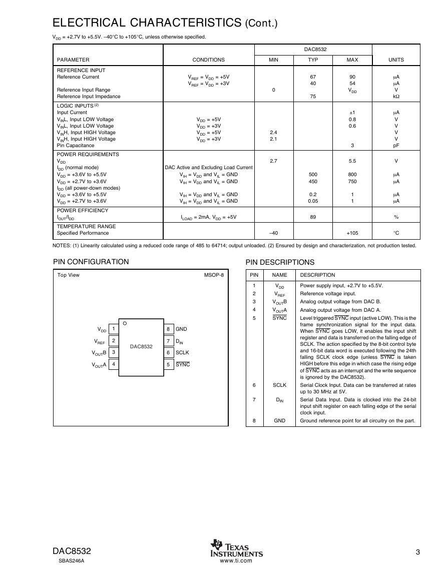
PIN CONFIGURATION
Top View
PIN DESCRIPTIONS
MSOP-8
PIN
NAME
DESCRIPTION
VDD
VREF
VOUTB
VOUTA
1
2
3
4
DAC8532
8
7
6
5
GND
DIN
SCLK
SYNC
1
2
3
4
5
6
7
8
VDD
VREF
VOUTB
VOUTA
SYNC
SCLK
DIN
GND
Power supply input, +2.7V to +5.5V.
Reference voltage input.
Analog output voltage from DAC B.
Analog output voltage from DAC A.
Level triggered SYNC input (active LOW). This is the
frame synchronization signal for the input data.
When SYNC goes LOW, it enables the input shift
register and data is transferred on the falling edge of
SCLK. The action specified by the 8-bit control byte
and 16-bit data word is executed following the 24th
falling SCLK clock edge (unless SYNC is taken
HIGH before this edge in which case the rising edge
of SYNC acts as an interrupt and the write sequence
is ignored by the DAC8532).
Serial Clock Input. Data can be transferred at rates
up to 30 MHz at 5V.
Serial Data Input. Data is clocked into the 24-bit
input shift register on each falling edge of the serial
clock input.
Ground reference point for all circuitry on the part.
DAC8532
SBAS246A
www.ti.com
3
�
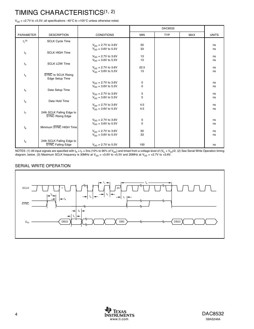
TIMING CHARACTERISTICS(1, 2)
VDD = +2.7V to +5.5V; all specifications –40°C to +105°C unless otherwise noted.
PARAMETER
DESCRIPTION
CONDITIONS
MIN
TYP
MAX
UNITS
DAC8532
(3)
t1
SCLK Cycle Time
t2
t3
t4
t5
t6
t7
t8
t9
SCLK HIGH Time
SCLK LOW Time
SYNC to SCLK Rising
Edge Setup Time
Data Setup Time
Data Hold Time
24th SCLK Falling Edge to
SYNC Rising Edge
Minimum SYNC HIGH Time
24th SCLK Falling Edge to
SYNC Falling Edge
VDD = 2.7V to 3.6V
VDD = 3.6V to 5.5V
VDD = 2.7V to 3.6V
VDD = 3.6V to 5.5V
VDD = 2.7V to 3.6V
VDD = 3.6V to 5.5V
VDD = 2.7V to 3.6V
VDD = 3.6V to 5.5V
VDD = 2.7V to 3.6V
VDD = 3.6V to 5.5V
VDD = 2.7V to 3.6V
VDD = 3.6V to 5.5V
VDD = 2.7V to 3.6V
VDD = 3.6V to 5.5V
VDD = 2.7V to 3.6V
VDD = 3.6V to 5.5V
VDD = 2.7V to 5.5V
50
33
13
13
22.5
13
0
0
5
5
4.5
4.5
0
0
50
33
100
ns
ns
ns
ns
ns
ns
ns
ns
ns
ns
ns
ns
ns
ns
ns
ns
ns
NOTES: (1) All input signals are specified with tR = tF = 5ns (10% to 90% of VDD) and timed from a voltage level of (VIL + VIH)/2. (2) See Serial Write Operation timing
diagram, below. (3) Maximum SCLK frequency is 30MHz at VDD = +3.6V to +5.5V and 20MHz at VDD = +2.7V to +3.6V.
SERIAL WRITE OPERATION
SCLK
SYNC
DIN
t1
t2
24
t7
t3
t9
t8
1
t4
t6
t5
DB23
DB0
DB23
4
www.ti.com
DAC8532
SBAS246A
�
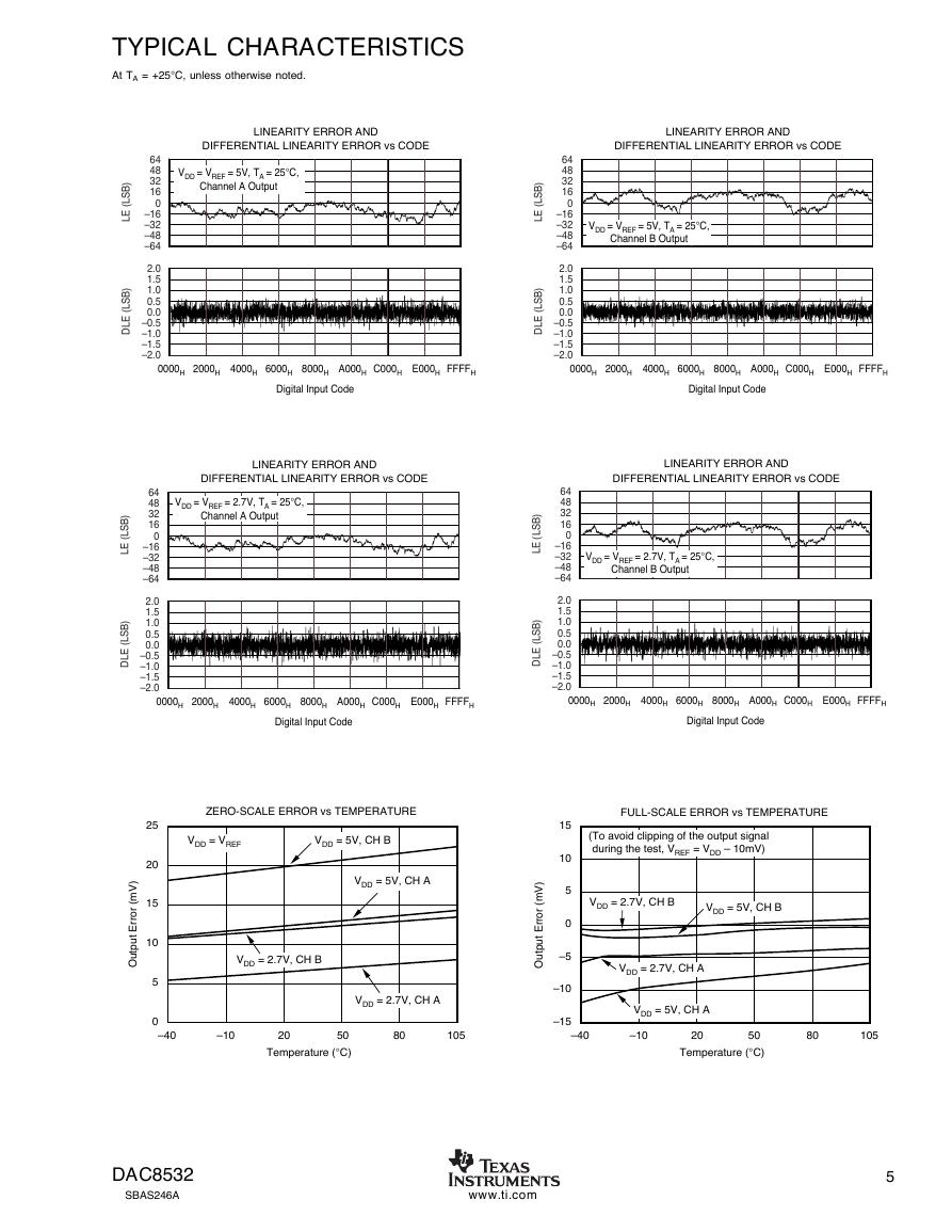
TYPICAL CHARACTERISTICS
At TA = +25°C, unless otherwise noted.
LINEARITY ERROR AND
DIFFERENTIAL LINEARITY ERROR vs CODE
LINEARITY ERROR AND
DIFFERENTIAL LINEARITY ERROR vs CODE
)
B
S
L
(
E
L
)
B
S
L
(
E
L
D
VDD = VREF = 5V, TA = 25°C,
Channel A Output
64
48
32
16
0
–16
–32
–48
–64
2.0
1.5
1.0
0.5
0.0
–0.5
–1.0
–1.5
–2.0
)
B
S
L
(
E
L
)
B
S
L
(
E
L
D
VDD = VREF = 5V, TA = 25°C,
Channel B Output
64
48
32
16
0
–16
–32
–48
–64
2.0
1.5
1.0
0.5
0.0
–0.5
–1.0
–1.5
–2.0
0000H 2000H 4000H 6000H 8000H
A000H C000H E000H FFFFH
0000H 2000H 4000H 6000H 8000H
A000H C000H E000H FFFFH
Digital Input Code
Digital Input Code
LINEARITY ERROR AND
DIFFERENTIAL LINEARITY ERROR vs CODE
LINEARITY ERROR AND
DIFFERENTIAL LINEARITY ERROR vs CODE
VDD = VREF = 2.7V, TA = 25°C,
Channel A Output
64
48
32
16
0
–16
–32
–48
–64
2.0
1.5
1.0
0.5
0.0
–0.5
–1.0
–1.5
–2.0
0000H 2000H 4000H 6000H 8000H
A000H C000H E000H FFFFH
VDD = VREF = 2.7V, TA = 25°C,
Channel B Output
)
B
S
L
(
E
L
)
B
S
L
(
E
L
D
64
48
32
16
0
–16
–32
–48
–64
2.0
1.5
1.0
0.5
0.0
–0.5
–1.0
–1.5
–2.0
0000H 2000H 4000H 6000H 8000H
A000H C000H E000H FFFFH
Digital Input Code
Digital Input Code
)
B
S
L
(
E
L
)
B
S
L
(
E
L
D
ZERO-SCALE ERROR vs TEMPERATURE
FULL-SCALE ERROR vs TEMPERATURE
25
20
15
10
5
)
V
m
(
r
o
r
r
E
t
u
p
t
u
O
VDD = VREF
VDD = 5V, CH B
VDD = 5V, CH A
VDD = 2.7V, CH B
VDD = 2.7V, CH A
)
V
m
(
r
o
r
r
E
t
u
p
t
u
O
15
10
5
0
–5
–10
–15
(To avoid clipping of the output signal
during the test, VREF = VDD – 10mV)
VDD = 2.7V, CH B
VDD = 5V, CH B
VDD = 2.7V, CH A
VDD = 5V, CH A
0
–40
–10
20
50
Temperature (°C)
80
105
–40
–10
20
50
Temperature (°C)
80
105
DAC8532
SBAS246A
www.ti.com
5
�
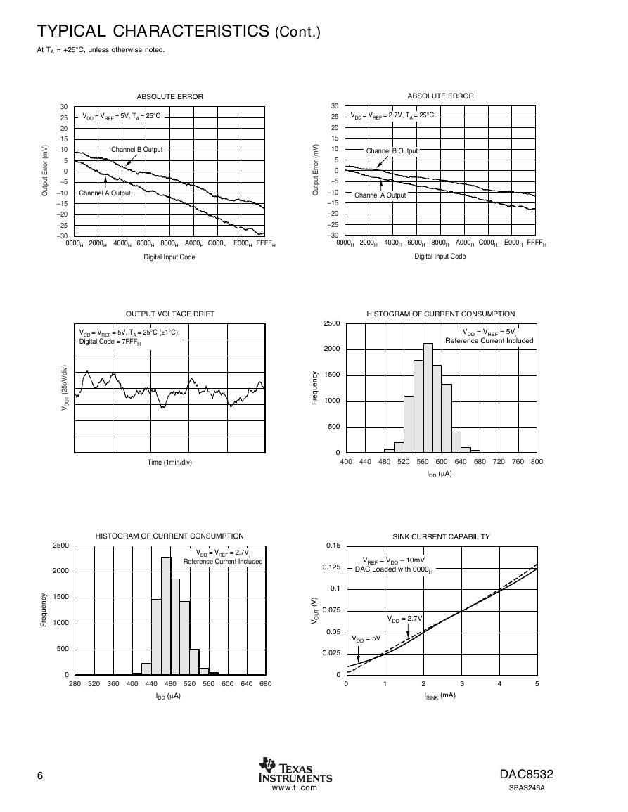
TYPICAL CHARACTERISTICS (Cont.)
At TA = +25°C, unless otherwise noted.
ABSOLUTE ERROR
ABSOLUTE ERROR
VDD = VREF = 5V, TA = 25°C
Channel B Output
Channel A Output
)
V
m
(
r
o
r
r
E
t
t
u
p
u
O
30
25
20
15
10
5
0
–5
–10
–15
–20
–25
–30
VDD = VREF = 2.7V, TA = 25°C
Channel B Output
Channel A Output
30
25
20
15
10
5
0
–5
–10
–15
–20
–25
–30
)
V
m
(
r
o
r
r
E
t
t
u
p
u
O
A000H C000H E000H FFFFH
0000H 2000H 4000H 6000H 8000H
0000H 2000H 4000H 6000H 8000H
A000H C000H E000H FFFFH
Digital Input Code
Digital Input Code
OUTPUT VOLTAGE DRIFT
HISTOGRAM OF CURRENT CONSUMPTION
VDD = VREF = 5V, TA = 25°C (±1°C),
Digital Code = 7FFFH
VDD = VREF = 5V,
Reference Current Included
2500
2000
y
c
n
e
u
q
e
r
F
1500
1000
500
0
i
)
v
d
/
V
µ
5
2
(
T
U
O
V
Time (1min/div)
400 440 480 520 560 600 640 680 720 760 800
IDD (µA)
HISTOGRAM OF CURRENT CONSUMPTION
SINK CURRENT CAPABILITY
VDD = VREF = 2.7V,
Reference Current Included
0.15
0.125
0.1
0.075
0.05
0.025
)
V
(
T
U
O
V
VREF = VDD – 10mV
DAC Loaded with 0000H
VDD = 2.7V
VDD = 5V
280 320 360 400 440 480 520 560 600 640 680
IDD (µA)
0
0
1
2
ISINK (mA)
3
4
5
www.ti.com
DAC8532
SBAS246A
2500
2000
y
c
n
e
u
q
e
r
F
1500
1000
500
0
6
�
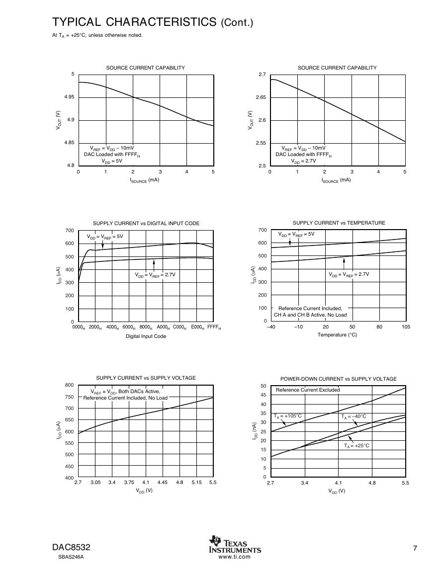
TYPICAL CHARACTERISTICS (Cont.)
At TA = +25°C, unless otherwise noted.
SOURCE CURRENT CAPABILITY
SOURCE CURRENT CAPABILITY
5
4.95
4.9
4.85
)
V
(
T
U
O
V
4.8
0
700
600
500
400
300
200
100
)
A
µ
(
D
D
I
2.7
2.65
2.6
2.55
)
V
(
T
U
O
V
2.5
0
VREF = VDD – 10mV
DAC Loaded with FFFFH
VDD = 5V
1
2
3
ISOURCE (mA)
4
5
VREF = VDD – 10mV
DAC Loaded with FFFFH
VDD = 2.7V
1
2
3
ISOURCE (mA)
4
5
SUPPLY CURRENT vs DIGITAL INPUT CODE
SUPPLY CURRENT vs TEMPERATURE
VDD = VREF = 5V
VDD = VREF = 2.7V
700
600
500
)
A
µ
(
D
D
I
400
300
200
100
VDD = VREF = 5V
VDD = VREF = 2.7V
Reference Current Included,
CH A and CH B Active, No Load
0
0000H 2000H 4000H 6000H 8000H
A000H C000H E000H FFFFH
0
–40
Digital Input Code
–10
20
50
Temperature (°C)
80
105
SUPPLY CURRENT vs SUPPLY VOLTAGE
POWER-DOWN CURRENT vs SUPPLY VOLTAGE
)
A
µ
(
D
D
I
800
750
700
650
600
550
500
450
400
VREF = VDD, Both DACs Active,
Reference Current Included, No Load
2.7
3.05
3.4
3.75
4.1
VDD (V)
4.45
4.8
5.15
5.5
)
A
n
(
D
D
I
50
45
40
35
30
25
20
15
10
5
0
Reference Current Excluded
TA = +105°C
TA = –40°C
TA = +25°C
2.7
3.4
4.1
VDD (V)
4.8
5.5
DAC8532
SBAS246A
www.ti.com
7
�
TYPICAL CHARACTERISTICS (Cont.)
At TA = +25°C, unless otherwise noted.
)
A
µ
(
D
D
I
1150
1050
950
850
750
650
550
450
3
2.5
2
1.5
1
0.5
0
1.5
1
0.5
0
)
V
(
T
U
O
V
)
V
(
T
U
O
V
8
SUPPLY CURRENT vs LOGIC INPUT VOLTAGE
TA = 25°C, SYNC Input (All Other Inputs = GND)
Reference Current Included,
CHA and CHB Active,
No Load
VDD = VREF = 5V
)
V
(
T
U
O
V
VDD = VREF = 2.7V
0
1
3
2
VLOGIC (V)
4
5
HALF-SCALE SETTLING TIME
(Large Signal)
VDD = VREF = 5V,
Output Loaded with
2kΩ and 200pF
to GND.
)
V
(
T
U
O
V
Time (2µs/div)
FULL-SCALE SETTLING TIME
(Large Signal)
VDD = VREF = 5V,
Output Loaded with
2kΩ and 200pF to
GND
Time (2µs/div)
FULL-SCALE SETTLING TIME
(Large Signal)
VDD = VREF = 2.7V,
Output Loaded with
2kΩ and 200pF
to GND.
Time (2µs/div)
5
4
3
2
1
0
3.5
3
2.5
2
1.5
1
0.5
0
HALF-SCALE SETTLING TIME
(Large Signal)
POWER-ON RESET TO ZERO-SCALE
VDD = VREF = 2.7V,
Output Loaded with
2kΩ and 200pF
to GND.
Loaded with 2kΩ to GND
VDD (2V/div)
VOUT (1V/div)
Time (2µs/div)
Time (100µs/div)
www.ti.com
DAC8532
SBAS246A
�


 V2版本原理图(Capacitive-Fingerprint-Reader-Schematic_V2).pdf
 摄像头工作原理.doc
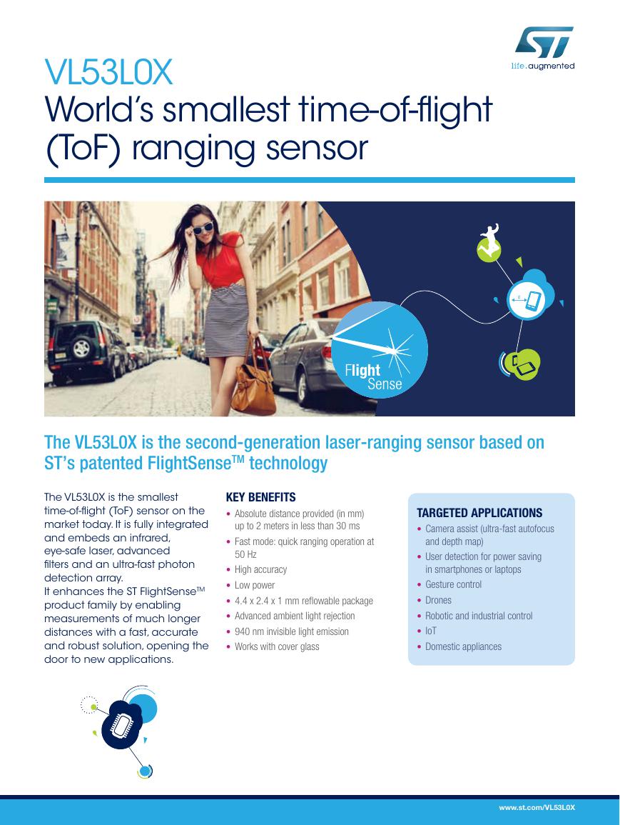 VL53L0X简要说明(En.FLVL53L00216).pdf
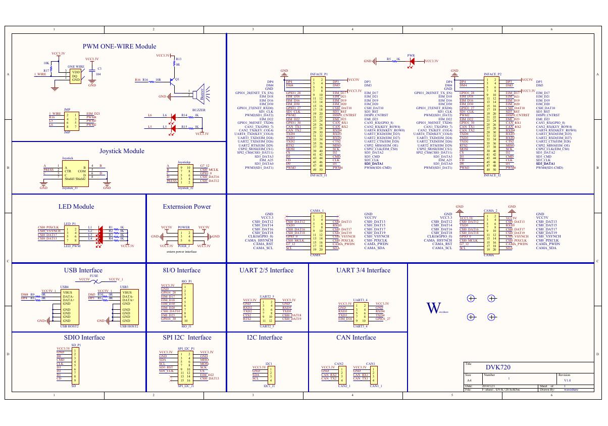 原理图(DVK720-Schematic).pdf
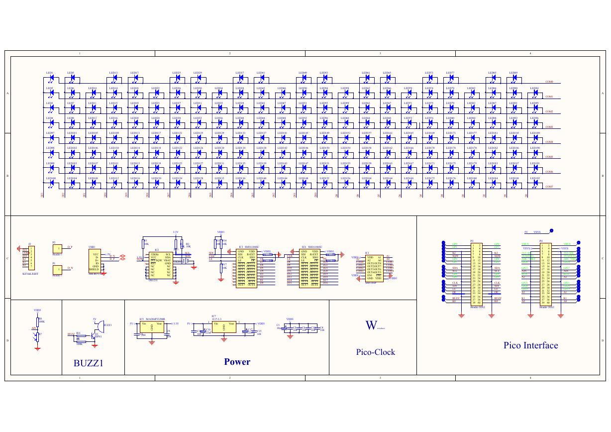 原理图(Pico-Clock-Green-Schdoc).pdf
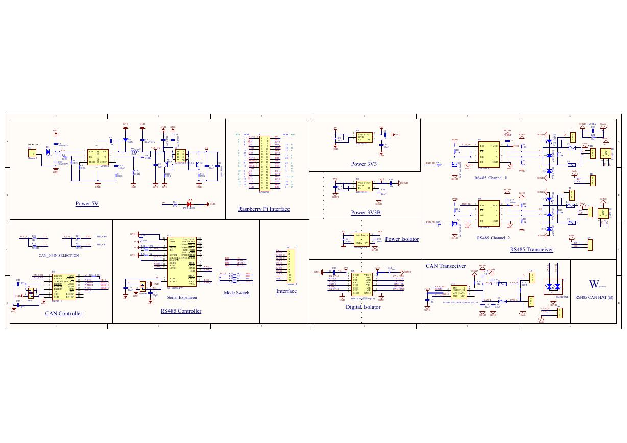 原理图(RS485-CAN-HAT-B-schematic).pdf
 File:SIM7500_SIM7600_SIM7800 Series_SSL_Application Note_V2.00.pdf
 ADS1263(Ads1262).pdf
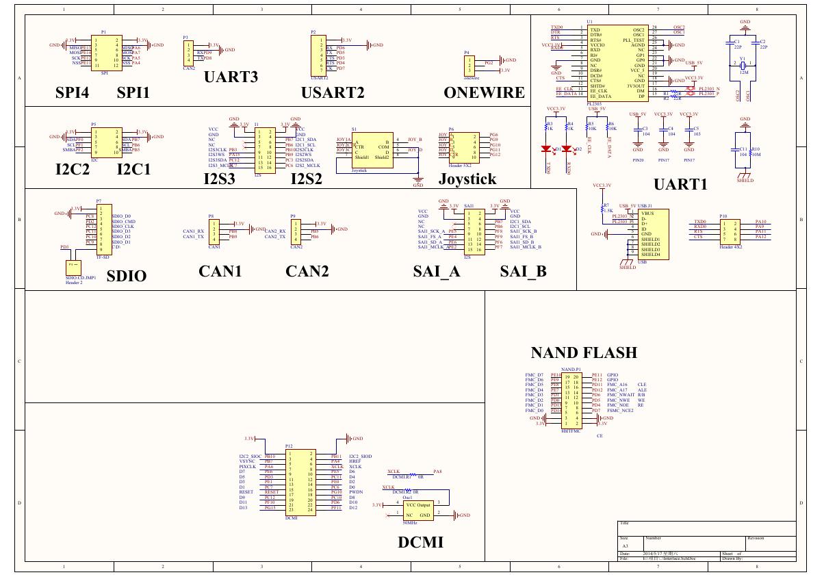 原理图(Open429Z-D-Schematic).pdf
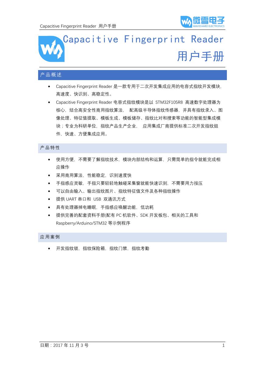 用户手册(Capacitive_Fingerprint_Reader_User_Manual_CN).pdf
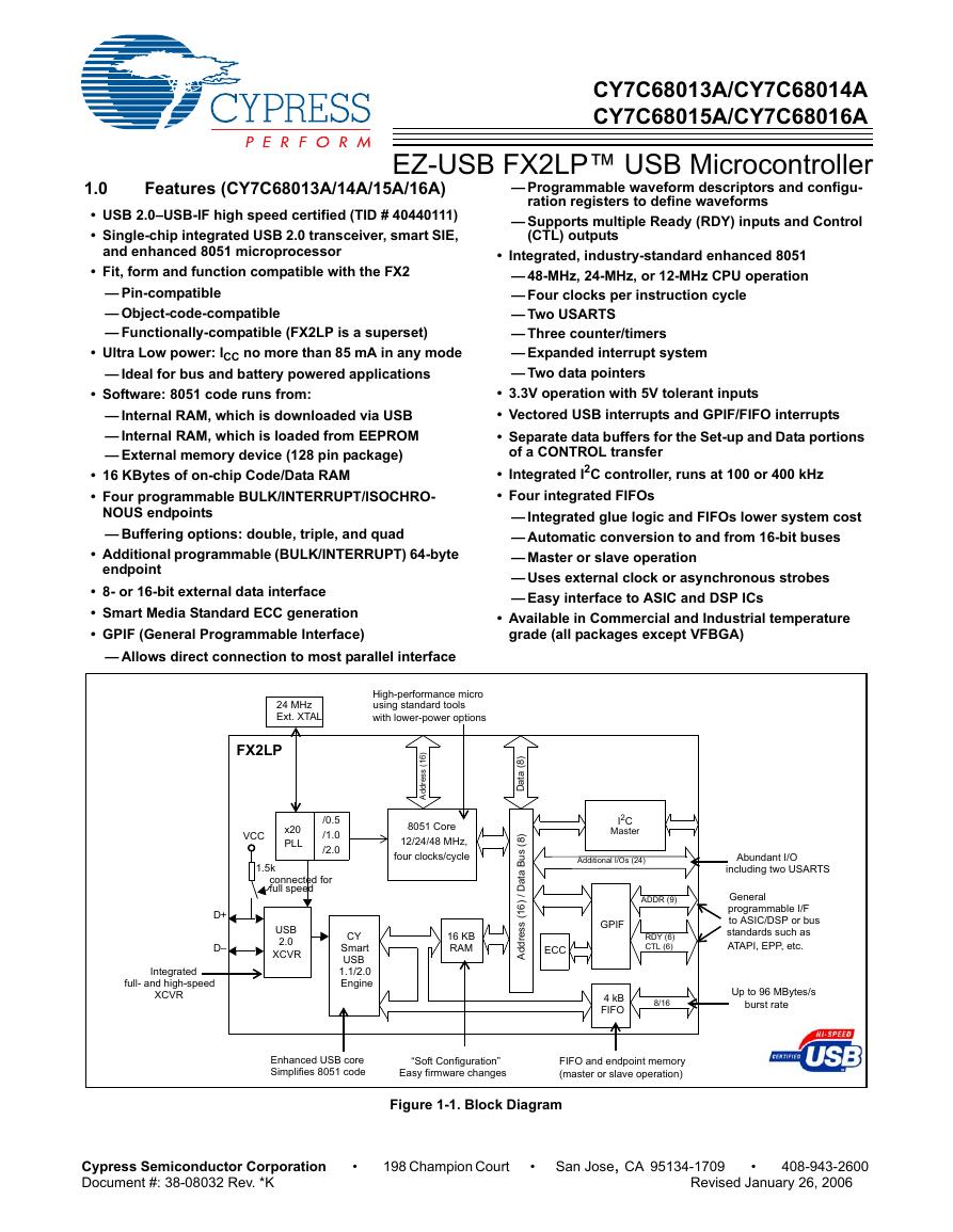 CY7C68013A(英文版)(CY7C68013A).pdf
 TechnicalReference_Dem.pdf