logo资料库

5G NR标准文件:3GPP TS 38.521-1 version 15.0.0 Release 15.pdf

第1页 / 共288页
第2页 / 共288页
第3页 / 共288页
第4页 / 共288页
第5页 / 共288页
第6页 / 共288页
第7页 / 共288页
第8页 / 共288页
资料共288页,剩余部分请下载后查看
Intellectual Property Rights
Foreword
Modal verbs terminology
Foreword
1 Scope
2 Reference
3 Definitions, symbols and abbreviations
3.1 Definitions
3.2 Symbols
3.3 Abbreviations
4 General
4.1 Relationship between minimum requirements and test requirements
4.2 Applicability of minimum requirements
4.3 Specification suffix information
4.4 Test points analysis
5 Operating bands and Channel arrangement
5.1 General
5.2 Operating bands
5.2A Operating bands for CA
5.2A.1 Intra-band CA
5.2A.2 Inter-band CA
5.2B Operating bands for DC
5.2B.1 General
5.2C Operating band combination for SUL
5.3 UE channel bandwidth
5.3.1 General
5.3.2 Maximum transmission bandwidth configuration
5.3.4 RB alignment with different numerologies
5.3.5 UE channel bandwidth per operating band
5.3.6 Asymmetric channel bandwidths
5.3A UE channel bandwidth for CA
5.3A.1 General
5.3A.2 Maximum transmission bandwidth configuration for CA
5.3A.3 Minimum guard band and transmission bandwidth configuration for CA
5.3A.4 RB alignment with Different Numerologies for CA
5.3A.5 UE channel bandwidth per operating band for CA
5.4 Channel arrangement
5.4.1 Channel spacing
5.4.1.1 Channel spacing for adjacent NR carriers
5.4.2 Channel raster
5.4.2.1 NR-ARFCN and channel raster
5.4.2.2 Channel raster to resource element mapping
5.4.2.3 Channel raster entries for each operating band
5.4.3 Synchronization raster
5.4.3.1 Synchronization raster and numbering
5.4.3.2 Synchronization raster to synchronization block resource element mapping
5.4.3.3 Synchronization raster entries for each operating band
5.4.4 TXŒRX frequency separation
5.4A Channel arrangement for CA
5.4A.1 Channel spacing for CA
5.4A.2 Channel raster for CA
5.4A.3 Synchronization raster for CA
5.4A.4 Tx-Rx frequency separation for CA
5.5 Configurations
5.5A Configurations for CA
5.5A.1 Configurations for intra-band contiguous CA
5.5A.2 Configurations for intra-band non-contiguous CA
5.5A.3 Configurations for inter-band CA
5.5B Configurations for DC
5.5C Configurations for SUL
6 Transmitter characteristics
6.1 General
6.2 Transmitter power
6.2.1 UE maximum output power
6.2.2 Maximum Power Reduction (MPR)
6.2.3 UE additional maximum output power reduction
6.2.4 Configured transmitted power
6.2A Transmitter power for CA
6.2B Transmitter power for DC
6.2C Transmitter power for SUL
6.2C.1 Configured transmitted power for SUL
6.2C.2 ?TIB,c
6.3 Output power dynamics
6.3.1 Minimum output power
6.3.2 Transmit OFF power
6.3.3 Transmit ON/OFF time mask
6.3.3.1 General
6.3.3.2 General ON/OFF time mask
6.3.3.3 Transmit power time mask for slot and [mini-slot] boundaries
6.3.3.4 PRACH time mask
6.3.3.5 PUCCH time mask
6.3.3.5.1 Long PUCCH time mask
6.3.3.5.2 Short PUCCH time mask
6.3.3.6 SRS time mask
6.3.3.7 PUSCH-PUCCH and PUSCH-SRS time masks
6.3.4 Power control
6.3.4.1 General
6.3.4.2 Absolute power tolerance
6.3.4.3 Power Control Relative power tolerance
6.3.4.4 Aggregate power tolerance
6.4 Transmit signal quality
6.4.1 Frequency error
6.4.2 Transmit modulation quality
6.4.2.1 Error Vector Magnitude
6.4.2.2 Carrier leakage
6.4.2.3 In-band emissions
6.4.2.4 EVM equalizer spectrum flatness
6.5 Output RF spectrum emissions
6.5.1 Occupied bandwidth
6.5.2 Out of band emission
6.5.2.1 General
6.5.2.2 Spectrum Emission Mask
6.5.2.3 Additional spectrum emission mask
6.5.2.4 Adjacent channel leakage ratio
6.5.2.4.1 NR ACLR
6.5.2.4.2 UTRA ACLR
6.5.3 Spurious emissions
6.5.3.1 General spurious emissions
6.5.3.2 Spurious emission for UE co-existence
6.5.3.3 Additional spurious emissions
6.5.4 Transmit intermodulation
7 Receiver characteristics
7.1 General
7.2 Diversity characteristics
7.3 Reference sensitivity
7.3.1 General
7.3.2 Reference sensitivity power level
7.3.2_1 Reference sensitivity level with 4 Rx antenna ports
7.3.3 ?RIB,c
7.3A Reference sensitivity for CA
7.3A.1 General
7.3A.2 Reference sensitivity power level for CA
7.3A.2.1 Intra-band contiguous CA
7.3A.2.1.0 Minimum requirements of reference sensitivity for CA
7.3A.2.1.1 Intra-band contiguous CA 2CC
7.3A.2.2 Intra-band non-contiguous CA
7.3A.2.3 Inter-band CA
7.3A.3 ?RIB,c for CA
7.3A.3.1 General
7.3A.3.2 Inter-band CA
7.3A.3.2.1 ?RIB,c for two bands
7.3A.3.2.2 ?RIB,c for three bands
7.3A.4 Reference sensitivity exceptions due to UL harmonic interference for CA
7.3B Reference sensitivity for DC
7.3C Reference sensitivity for SUL
7.3C.1 General
7.3C.2 Reference sensitivity power level
7.3C.3 ?RIB,c for SUL
7.3C.3.1 General
7.3C.3.2 SUL band combination
7.4 Maximum input level
7.4A Maximum input level for CA
7.5 Adjacent channel selectivity
7.5A Adjacent channel selectivity for CA
7.6 Blocking characteristics
7.6.1 General
7.6.2 Inband Blocking
7.6.3 Out-of-band blocking
7.6.4 Narrow band blocking
7.6A Blocking characteristics for CA
7.6A.1 General
7.6A.2 Inband blocking for CA
7.6A.2.1 Intra-band contiguous CA
7.6A.3 Out-of-band blocking for CA
7.6A.3.1 Intra-band contiguous CA
7.6A.4 Narrow band blocking for CA
7.7 Spurious response
7.8 Intermodulation characteristics
7.9 Spurious emissions
Annex A (normative): Measurement channels
A.1 General
A.2 UL reference measurement channels
A.2.1 General
A.2.2 Reference measurement channels for FDD
A.2.2.1 DFT-s-OFDM Pi/2-BPSK
A.2.2.2 DFT-s-OFDM QPSK
A.2.2.3 DFT-s-OFDM 16QAM
A.2.2.4 DFT-s-OFDM 64QAM
A.2.2.5 DFT-s-OFDM 256QAM
A.2.2.6 CP-OFDM QPSK
A.2.2.7 CP-OFDM 16QAM
A.2.2.8 CP-OFDM 64QAM
A.2.2.9 CP-OFDM 256QAM
A.2.3 Reference measurement channels for TDD
A.2.3.1 DFT-s-OFDM Pi/2-BPSK
A.2.3.2 DFT-s-OFDM QPSK
A.2.3.3 DFT-s-OFDM 16QAM
A.2.3.4 DFT-s-OFDM 64QAM
A.2.3.5 DFT-s-OFDM 256QAM
A.2.3.6 CP-OFDM QPSK
A.2.3.7 CP-OFDM 16QAM
A.2.3.8 CP-OFDM 64QAM
A.2.3.9 CP-OFDM 256QAM
A.3 DL reference measurement channels
A.3.1 General
A.3.2 DL reference measurement channels for FDD
A.3.2.1 General
A.3.2.2 FRC for receiver requirements for QPSK
A.3.2.3 FRC for maximum input level for 64QAM
A.3.2.4 FRC for maximum input level for 256 QAM
A.3.3 DL reference measurement channels for TDD
A.3.3.1 General
A.3.3.2 FRC for receiver requirements for QPSK
A.3.3.3 FRC for maximum input level for 64QAM
A.3.3.4 FRC for maximum input level for 256 QAM
A.4 CSI reference measurement channels
A.5 OFDMA Channel Noise Generator (OCNG)
A.5.1 OCNG Patterns for FDD
A.5.1.1 OCNG FDD pattern 1: Generic OCNG FDD Pattern for all unused REs
A.5.2 OCNG Patterns for TDD
A.5.2.1 OCNG TDD pattern 1: Generic OCNG TDD Pattern for all unused REs
Annex B (normative): Propagation Conditions
B.0 No interference
Annex C (normative): Downlink physical channels
C.0 Downlink signal levels
C.1 General
C.2 Setup
C.3 Connection
C.3.1 Measurement of Receiver Characteristics
Annex E (normative): Global In-Channel TX-Test
E.1 General
E.2 Signals and results
E.2.1 Basic principle
E.2.2 Output signal of the TX under test
E.2.3 Reference signal
E.2.4 Measurement results
E.2.5 Measurement points
E.3 Signal processing
E.3.1 Pre FFT minimization process
E.3.2 Timing of the FFT window
E.3.3 Post FFT equalisation
E.4 Derivation of the results
E.4.1 EVM
E.4.2 Averaged EVM
E.4.3 In-band emissions measurement
E.4.4 EVM equalizer spectrum flatness
E.4.5 Frequency error and Carrier leakage
E.4.6 EVM of Demodulation reference symbols (EVMDMRS)
E.4.6.1 1st average for EVM DMRS
E.4.6.2 Final average for EVM DMRS
E.5 EVM and inband emissions for PUCCH
E.5.1 Basic principle
E.5.2 Output signal of the TX under test
E.5.3 Reference signal
E.5.4 Measurement results
E.5.5 Measurement points
E.5.6 Pre FFT minimization process
E.5.7 Timing of the FFT window
E.5.8 Post FFT equalisation
E.5.9 Derivation of the results
E.5.9.1 EVMPUCCH
E.5.9.2 Averaged EVMPUCCH
E.5.9.3 In-band emissions measurement
E.6 EVM for PRACH
E.6.1 Basic principle
E.6.2 Output signal of the TX under test
E.6.3 Reference signal
E.6.4 Measurement results
E.6.5 Measurement points
E.6.6 Pre FFT minimization process
E.6.7 Timing of the FFT window
E.6.8 Post FFT equalisation
E.6.9 Derivation of the results
E.6.9.1 EVMPRACH
E.6.9.2 Averaged EVMPRACH
Annex F (normative): Measurement uncertainties and Test Tolerances
F.1 Acceptable uncertainty of Test System (normative)
F.1.1 Measurement of test environments
F.1.2 Measurement of transmitter
F.1.3 Measurement of receiver
F.2 Interpretation of measurement results (normative)
F.3 Test Tolerance and Derivation of Test Requirements (informative)
F.3.1 Measurement of test environments
F.3.2 Measurement of transmitter
F.3.3 Measurement of receiver
Annex G (normative): Uplink Physical Channels
G.0 Uplink Signal Levels
G.1 General
G.2 Set-up
G.3 Connection
G.3.0 Measurement of Transmitter Characteristics
G.3.1 Measurement of Receiver Characteristics
G.3.2 Measurement of Performance Requirements
Annex H (normative): Statistical Testing
H.1 General
H.2 Statistical testing of receiver characteristics
H.2.1 General
H.2.2 Mapping throughput to error ratio
H.2.3 Design of the test
H.2.4 Numerical definition of the pass fail limits
H.2.5 Pass fail decision rules
Annex I: Change history
History
ETSI TS 138 521-1 V15.0.0 (2018-10) TECHNICAL SPECIFICATION User Equipment (UE) conformance specification; 5G; NR; Radio transmission and reception; Part 1: Range 1 Standalone (3GPP TS 38.521-1 version 15.0.0 Release 15)
3GPP TS 38.521-1 version 15.0.0 Release 15 1 ETSI TS 138 521-1 V15.0.0 (2018-10) Reference DTS/TSGR-0538521-1vf00 Keywords 5G ETSI 650 Route des Lucioles F-06921 Sophia Antipolis Cedex - FRANCE Tel.: +33 4 92 94 42 00 Fax: +33 4 93 65 47 16 Siret N° 348 623 562 00017 - NAF 742 C Association à but non lucratif enregistrée à la Sous-Préfecture de Grasse (06) N° 7803/88 Important notice The present document can be downloaded from: http://www.etsi.org/standards-search The present document may be made available in electronic versions and/or in print. The content of any electronic and/or print versions of the present document shall not be modified without the prior written authorization of ETSI. In case of any existing or perceived difference in contents between such versions and/or in print, the only prevailing document is the print of the Portable Document Format (PDF) version kept on a specific network drive within ETSI Secretariat. Users of the present document should be aware that the document may be subject to revision or change of status. Information on the current status of this and other ETSI documents is available at https://portal.etsi.org/TB/ETSIDeliverableStatus.aspx If you find errors in the present document, please send your comment to one of the following services: https://portal.etsi.org/People/CommiteeSupportStaff.aspx Copyright Notification No part may be reproduced or utilized in any form or by any means, electronic or mechanical, including photocopying and microfilm except as authorized by written permission of ETSI. The content of the PDF version shall not be modified without the written authorization of ETSI. The copyright and the foregoing restriction extend to reproduction in all media. © ETSI 2018. All rights reserved. DECTTM, PLUGTESTSTM, UMTSTM and the ETSI logo are trademarks of ETSI registered for the benefit of its Members. 3GPPTM and LTETM are trademarks of ETSI registered for the benefit of its Members and of the 3GPP Organizational Partners. oneM2M logo is protected for the benefit of its Members. GSM® and the GSM logo are trademarks registered and owned by the GSM Association. ETSI
3GPP TS 38.521-1 version 15.0.0 Release 15 2 ETSI TS 138 521-1 V15.0.0 (2018-10) Intellectual Property Rights Essential patents IPRs essential or potentially essential to normative deliverables may have been declared to ETSI. The information pertaining to these essential IPRs, if any, is publicly available for ETSI members and non-members, and can be found in ETSI SR 000 314: "Intellectual Property Rights (IPRs); Essential, or potentially Essential, IPRs notified to ETSI in respect of ETSI standards", which is available from the ETSI Secretariat. Latest updates are available on the ETSI Web server (https://ipr.etsi.org/). Pursuant to the ETSI IPR Policy, no investigation, including IPR searches, has been carried out by ETSI. No guarantee can be given as to the existence of other IPRs not referenced in ETSI SR 000 314 (or the updates on the ETSI Web server) which are, or may be, or may become, essential to the present document. Trademarks The present document may include trademarks and/or tradenames which are asserted and/or registered by their owners. ETSI claims no ownership of these except for any which are indicated as being the property of ETSI, and conveys no right to use or reproduce any trademark and/or tradename. Mention of those trademarks in the present document does not constitute an endorsement by ETSI of products, services or organizations associated with those trademarks. Foreword This Technical Specification (TS) has been produced by ETSI 3rd Generation Partnership Project (3GPP). The present document may refer to technical specifications or reports using their 3GPP identities, UMTS identities or GSM identities. These should be interpreted as being references to the corresponding ETSI deliverables. The cross reference between GSM, UMTS, 3GPP and ETSI identities can be found under http://webapp.etsi.org/key/queryform.asp. Modal verbs terminology In the present document "shall", "shall not", "should", "should not", "may", "need not", "will", "will not", "can" and "cannot" are to be interpreted as described in clause 3.2 of the ETSI Drafting Rules (Verbal forms for the expression of provisions). "must" and "must not" are NOT allowed in ETSI deliverables except when used in direct citation. ETSI
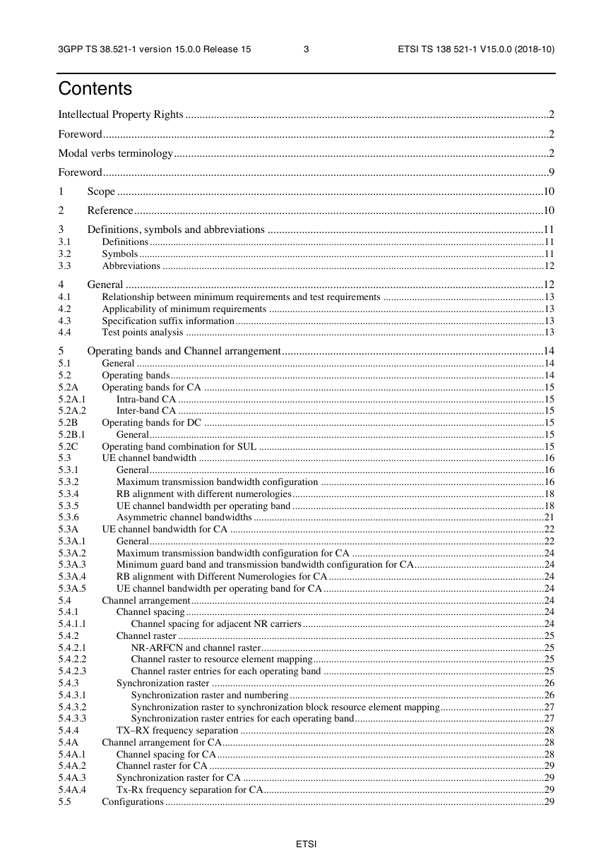
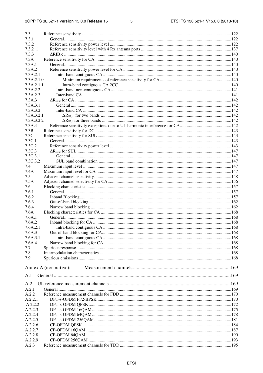
3GPP TS 38.521-1 version 15.0.0 Release 15 3 ETSI TS 138 521-1 V15.0.0 (2018-10) Contents Intellectual Property Rights ................................................................................................................................ 2 Foreword ............................................................................................................................................................. 2 Modal verbs terminology .................................................................................................................................... 2 Foreword ............................................................................................................................................................. 9 1 2 3 3.1 3.2 3.3 4 4.1 4.2 4.3 4.4 Scope ...................................................................................................................................................... 10 Reference ................................................................................................................................................ 10 Definitions, symbols and abbreviations ................................................................................................. 11 Definitions ........................................................................................................................................................ 11 Symbols ............................................................................................................................................................ 11 Abbreviations ................................................................................................................................................... 12 General ................................................................................................................................................... 12 Relationship between minimum requirements and test requirements .............................................................. 13 Applicability of minimum requirements .......................................................................................................... 13 Specification suffix information ....................................................................................................................... 13 Test points analysis .......................................................................................................................................... 13 5 5.1 5.2 5.2A 5.2A.1 5.2A.2 5.2B 5.2B.1 5.2C 5.3 5.3.1 5.3.2 5.3.4 5.3.5 5.3.6 5.3A 5.3A.1 5.3A.2 5.3A.3 5.3A.4 5.3A.5 5.4 5.4.1 5.4.1.1 5.4.2 5.4.2.1 5.4.2.2 5.4.2.3 5.4.3 5.4.3.1 5.4.3.2 5.4.3.3 5.4.4 5.4A 5.4A.1 5.4A.2 5.4A.3 5.4A.4 5.5 Operating bands and Channel arrangement ............................................................................................ 14 General ............................................................................................................................................................. 14 Operating bands ................................................................................................................................................ 14 Operating bands for CA ................................................................................................................................... 15 Intra-band CA ............................................................................................................................................. 15 Inter-band CA ............................................................................................................................................. 15 Operating bands for DC ................................................................................................................................... 15 General ........................................................................................................................................................ 15 Operating band combination for SUL .............................................................................................................. 15 UE channel bandwidth ..................................................................................................................................... 16 General ........................................................................................................................................................ 16 Maximum transmission bandwidth configuration ...................................................................................... 16 RB alignment with different numerologies ................................................................................................. 18 UE channel bandwidth per operating band ................................................................................................. 18 Asymmetric channel bandwidths ................................................................................................................ 21 UE channel bandwidth for CA ......................................................................................................................... 22 General ........................................................................................................................................................ 22 Maximum transmission bandwidth configuration for CA .......................................................................... 24 Minimum guard band and transmission bandwidth configuration for CA.................................................. 24 RB alignment with Different Numerologies for CA ................................................................................... 24 UE channel bandwidth per operating band for CA ..................................................................................... 24 Channel arrangement ........................................................................................................................................ 24 Channel spacing .......................................................................................................................................... 24 Channel spacing for adjacent NR carriers ............................................................................................. 24 Channel raster ............................................................................................................................................. 25 NR-ARFCN and channel raster............................................................................................................. 25 Channel raster to resource element mapping......................................................................................... 25 Channel raster entries for each operating band ..................................................................................... 25 Synchronization raster ................................................................................................................................ 26 Synchronization raster and numbering .................................................................................................. 26 Synchronization raster to synchronization block resource element mapping ........................................ 27 Synchronization raster entries for each operating band......................................................................... 27 TX–RX frequency separation ..................................................................................................................... 28 Channel arrangement for CA............................................................................................................................ 28 Channel spacing for CA .............................................................................................................................. 28 Channel raster for CA ................................................................................................................................. 29 Synchronization raster for CA .................................................................................................................... 29 Tx-Rx frequency separation for CA............................................................................................................ 29 Configurations .................................................................................................................................................. 29 ETSI
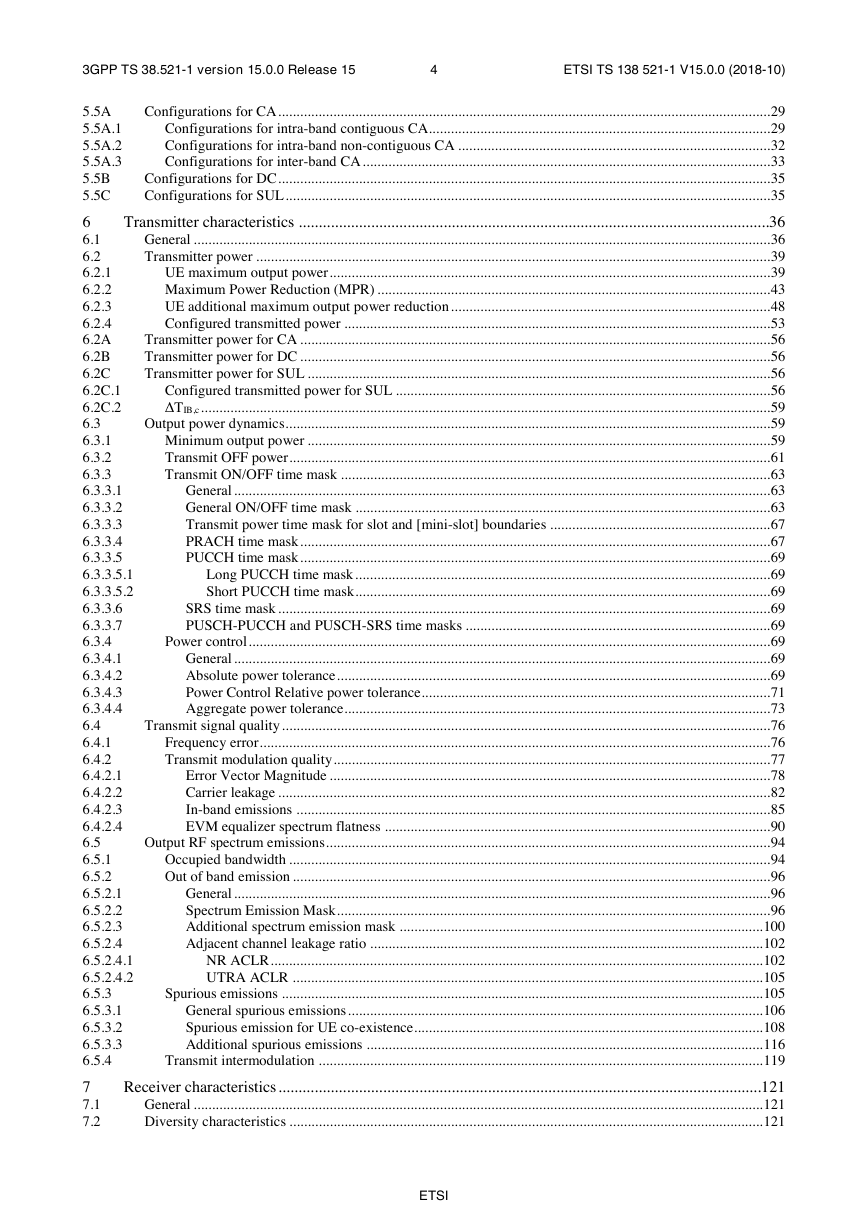
3GPP TS 38.521-1 version 15.0.0 Release 15 4 ETSI TS 138 521-1 V15.0.0 (2018-10) 5.5A 5.5A.1 5.5A.2 5.5A.3 5.5B 5.5C Configurations for CA ...................................................................................................................................... 29 Configurations for intra-band contiguous CA............................................................................................. 29 Configurations for intra-band non-contiguous CA ..................................................................................... 32 Configurations for inter-band CA ............................................................................................................... 33 Configurations for DC ...................................................................................................................................... 35 Configurations for SUL .................................................................................................................................... 35 6 6.1 6.2 6.2.1 6.2.2 6.2.3 6.2.4 6.2A 6.2B 6.2C 6.2C.1 6.2C.2 6.3 6.3.1 6.3.2 6.3.3 6.3.3.1 6.3.3.2 6.3.3.3 6.3.3.4 6.3.3.5 6.3.3.5.1 6.3.3.5.2 6.3.3.6 6.3.3.7 6.3.4 6.3.4.1 6.3.4.2 6.3.4.3 6.3.4.4 6.4 6.4.1 6.4.2 6.4.2.1 6.4.2.2 6.4.2.3 6.4.2.4 6.5 6.5.1 6.5.2 6.5.2.1 6.5.2.2 6.5.2.3 6.5.2.4 6.5.2.4.1 6.5.2.4.2 6.5.3 6.5.3.1 6.5.3.2 6.5.3.3 6.5.4 Transmitter characteristics ..................................................................................................................... 36 General ............................................................................................................................................................. 36 Transmitter power ............................................................................................................................................ 39 UE maximum output power ........................................................................................................................ 39 Maximum Power Reduction (MPR) ........................................................................................................... 43 UE additional maximum output power reduction ....................................................................................... 48 Configured transmitted power .................................................................................................................... 53 Transmitter power for CA ................................................................................................................................ 56 Transmitter power for DC ................................................................................................................................ 56 Transmitter power for SUL .............................................................................................................................. 56 Configured transmitted power for SUL ...................................................................................................... 56 ΔTIB,c ........................................................................................................................................................... 59 Output power dynamics .................................................................................................................................... 59 Minimum output power .............................................................................................................................. 59 Transmit OFF power ................................................................................................................................... 61 Transmit ON/OFF time mask ..................................................................................................................... 63 General .................................................................................................................................................. 63 General ON/OFF time mask ................................................................................................................. 63 Transmit power time mask for slot and [mini-slot] boundaries ............................................................ 67 PRACH time mask ................................................................................................................................ 67 PUCCH time mask ................................................................................................................................ 69 Long PUCCH time mask ................................................................................................................. 69 Short PUCCH time mask ................................................................................................................. 69 SRS time mask ...................................................................................................................................... 69 PUSCH-PUCCH and PUSCH-SRS time masks ................................................................................... 69 Power control .............................................................................................................................................. 69 General .................................................................................................................................................. 69 Absolute power tolerance ...................................................................................................................... 69 Power Control Relative power tolerance ............................................................................................... 71 Aggregate power tolerance.................................................................................................................... 73 Transmit signal quality ..................................................................................................................................... 76 Frequency error ........................................................................................................................................... 76 Transmit modulation quality ....................................................................................................................... 77 Error Vector Magnitude ........................................................................................................................ 78 Carrier leakage ...................................................................................................................................... 82 In-band emissions ................................................................................................................................. 85 EVM equalizer spectrum flatness ......................................................................................................... 90 Output RF spectrum emissions ......................................................................................................................... 94 Occupied bandwidth ................................................................................................................................... 94 Out of band emission .................................................................................................................................. 96 General .................................................................................................................................................. 96 Spectrum Emission Mask ...................................................................................................................... 96 Additional spectrum emission mask ................................................................................................... 100 Adjacent channel leakage ratio ........................................................................................................... 102 NR ACLR ...................................................................................................................................... 102 UTRA ACLR ................................................................................................................................ 105 Spurious emissions ................................................................................................................................... 105 General spurious emissions ................................................................................................................. 106 Spurious emission for UE co-existence............................................................................................... 108 Additional spurious emissions ............................................................................................................ 116 Transmit intermodulation ......................................................................................................................... 119 7 7.1 7.2 Receiver characteristics ........................................................................................................................ 121 General ........................................................................................................................................................... 121 Diversity characteristics ................................................................................................................................. 121 ETSI
3GPP TS 38.521-1 version 15.0.0 Release 15 5 ETSI TS 138 521-1 V15.0.0 (2018-10) 7.3 7.3.1 7.3.2 7.3.2_1 7.3.3 7.3A 7.3A.1 7.3A.2 7.3A.2.1 7.3A.2.1.0 7.3A.2.1.1 7.3A.2.2 7.3A.2.3 7.3A.3 7.3A.3.1 7.3A.3.2 7.3A.3.2.1 7.3A.3.2.2 7.3A.4 7.3B 7.3C 7.3C.1 7.3C.2 7.3C.3 7.3C.3.1 7.3C.3.2 7.4 7.4A 7.5 7.5A 7.6 7.6.1 7.6.2 7.6.3 7.6.4 7.6A 7.6A.1 7.6A.2 7.6A.2.1 7.6A.3 7.6A.3.1 7.6A.4 7.7 7.8 7.9 Reference sensitivity ...................................................................................................................................... 122 General ...................................................................................................................................................... 122 Reference sensitivity power level ............................................................................................................. 122 Reference sensitivity level with 4 Rx antenna ports ................................................................................. 137 ΔRIB,c ...................................................................................................................................................... 140 Reference sensitivity for CA .......................................................................................................................... 140 General ...................................................................................................................................................... 140 Reference sensitivity power level for CA ................................................................................................. 140 Intra-band contiguous CA ................................................................................................................... 140 Minimum requirements of reference sensitivity for CA ................................................................ 140 Intra-band contiguous CA 2CC ..................................................................................................... 140 Intra-band non-contiguous CA ............................................................................................................ 141 Inter-band CA ..................................................................................................................................... 141 ΔRIB,c for CA ............................................................................................................................................ 142 General ................................................................................................................................................ 142 Inter-band CA ..................................................................................................................................... 142 ΔRIB,c for two bands ..................................................................................................................... 142 ΔRIB,c for three bands .................................................................................................................... 142 Reference sensitivity exceptions due to UL harmonic interference for CA .............................................. 142 Reference sensitivity for DC .......................................................................................................................... 143 Reference sensitivity for SUL ........................................................................................................................ 143 General ...................................................................................................................................................... 143 Reference sensitivity power level ............................................................................................................. 143 ΔRIB,c for SUL .......................................................................................................................................... 147 General ................................................................................................................................................ 147 SUL band combination ....................................................................................................................... 147 Maximum input level ..................................................................................................................................... 147 Maximum input level for CA ......................................................................................................................... 147 Adjacent channel selectivity ........................................................................................................................... 148 Adjacent channel selectivity for CA ............................................................................................................... 156 Blocking characteristics ................................................................................................................................. 157 General ...................................................................................................................................................... 157 Inband Blocking ........................................................................................................................................ 157 Out-of-band blocking ................................................................................................................................ 162 Narrow band blocking .............................................................................................................................. 162 Blocking characteristics for CA ..................................................................................................................... 168 General ...................................................................................................................................................... 168 Inband blocking for CA ............................................................................................................................ 168 Intra-band contiguous CA ................................................................................................................... 168 Out-of-band blocking for CA.................................................................................................................... 168 Intra-band contiguous CA ................................................................................................................... 168 Narrow band blocking for CA .................................................................................................................. 168 Spurious response ........................................................................................................................................... 168 Intermodulation characteristics ...................................................................................................................... 168 Spurious emissions ......................................................................................................................................... 168 Annex A (normative): Measurement channels ................................................................................ 169 A.1 General ................................................................................................................................................. 169 A.2 UL reference measurement channels ................................................................................................... 169 General ........................................................................................................................................................... 169 A.2.1 Reference measurement channels for FDD .................................................................................................... 170 A.2.2 A.2.2.1 DFT-s-OFDM Pi/2-BPSK ........................................................................................................................ 170 DFT-s-OFDM QPSK ................................................................................................................................ 172 A.2.2.2 DFT-s-OFDM 16QAM ............................................................................................................................. 175 A.2.2.3 DFT-s-OFDM 64QAM ............................................................................................................................. 178 A.2.2.4 DFT-s-OFDM 256QAM ........................................................................................................................... 181 A.2.2.5 A.2.2.6 CP-OFDM QPSK ..................................................................................................................................... 184 CP-OFDM 16QAM .................................................................................................................................. 187 A.2.2.7 CP-OFDM 64QAM .................................................................................................................................. 190 A.2.2.8 A.2.2.9 CP-OFDM 256QAM ................................................................................................................................ 193 Reference measurement channels for TDD .................................................................................................... 195 A.2.3 ETSI
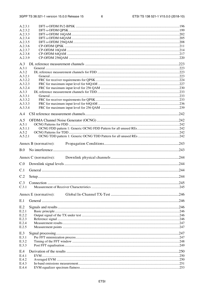
3GPP TS 38.521-1 version 15.0.0 Release 15 6 ETSI TS 138 521-1 V15.0.0 (2018-10) A.2.3.1 A.2.3.2 A.2.3.3 A.2.3.4 A.2.3.5 A.2.3.6 A.2.3.7 A.2.3.8 A.2.3.9 DFT-s-OFDM Pi/2-BPSK ........................................................................................................................ 196 DFT-s-OFDM QPSK ................................................................................................................................ 199 DFT-s-OFDM 16QAM ............................................................................................................................. 202 DFT-s-OFDM 64QAM ............................................................................................................................. 205 DFT-s-OFDM 256QAM ........................................................................................................................... 208 CP-OFDM QPSK ..................................................................................................................................... 211 CP-OFDM 16QAM .................................................................................................................................. 214 CP-OFDM 64QAM .................................................................................................................................. 217 CP-OFDM 256QAM ................................................................................................................................ 220 A.3 DL reference measurement channels ................................................................................................... 223 General ........................................................................................................................................................... 223 A.3.1 DL reference measurement channels for FDD ............................................................................................... 223 A.3.2 General ...................................................................................................................................................... 223 A.3.2.1 A.3.2.2 FRC for receiver requirements for QPSK ................................................................................................. 224 FRC for maximum input level for 64QAM .............................................................................................. 227 A.3.2.3 A.3.2.4 FRC for maximum input level for 256 QAM ........................................................................................... 230 DL reference measurement channels for TDD ............................................................................................... 233 A.3.3 A.3.3.1 General ...................................................................................................................................................... 233 FRC for receiver requirements for QPSK ................................................................................................. 233 A.3.3.2 FRC for maximum input level for 64QAM .............................................................................................. 236 A.3.3.3 A.3.3.4 FRC for maximum input level for 256 QAM ........................................................................................... 239 A.4 CSI reference measurement channels ................................................................................................... 242 A.5 OFDMA Channel Noise Generator (OCNG) ....................................................................................... 242 OCNG Patterns for FDD ................................................................................................................................ 242 A.5.1 A.5.1.1 OCNG FDD pattern 1: Generic OCNG FDD Pattern for all unused REs................................................. 242 OCNG Patterns for TDD ................................................................................................................................ 242 A.5.2 OCNG TDD pattern 1: Generic OCNG TDD Pattern for all unused REs ................................................ 242 A.5.2.1 Propagation Conditions ............................................................................... 243 Annex B (normative): B.0 No interference ..................................................................................................................................... 243 Annex C (normative): Downlink physical channels ........................................................................ 244 C.0 Downlink signal levels ......................................................................................................................... 244 C.1 General ................................................................................................................................................. 244 C.2 Setup ..................................................................................................................................................... 244 C.3 Connection ........................................................................................................................................... 245 Measurement of Receiver Characteristics ...................................................................................................... 245 C.3.1 Annex E (normative): Global In-Channel TX-Test ........................................................................ 246 E.1 General ................................................................................................................................................. 246 E.2 Signals and results ................................................................................................................................ 246 Basic principle ................................................................................................................................................ 246 E.2.1 E.2.2 Output signal of the TX under test ................................................................................................................. 246 Reference signal ............................................................................................................................................. 246 E.2.3 Measurement results ....................................................................................................................................... 247 E.2.4 E.2.5 Measurement points ....................................................................................................................................... 247 E.3 Signal processing .................................................................................................................................. 247 Pre FFT minimization process........................................................................................................................ 247 E.3.1 Timing of the FFT window ............................................................................................................................ 248 E.3.2 E.3.3 Post FFT equalisation ..................................................................................................................................... 249 E.4 Derivation of the results ....................................................................................................................... 250 EVM ............................................................................................................................................................... 250 E.4.1 Averaged EVM .............................................................................................................................................. 250 E.4.2 In-band emissions measurement ..................................................................................................................... 251 E.4.3 E.4.4 EVM equalizer spectrum flatness ................................................................................................................... 253 ETSI
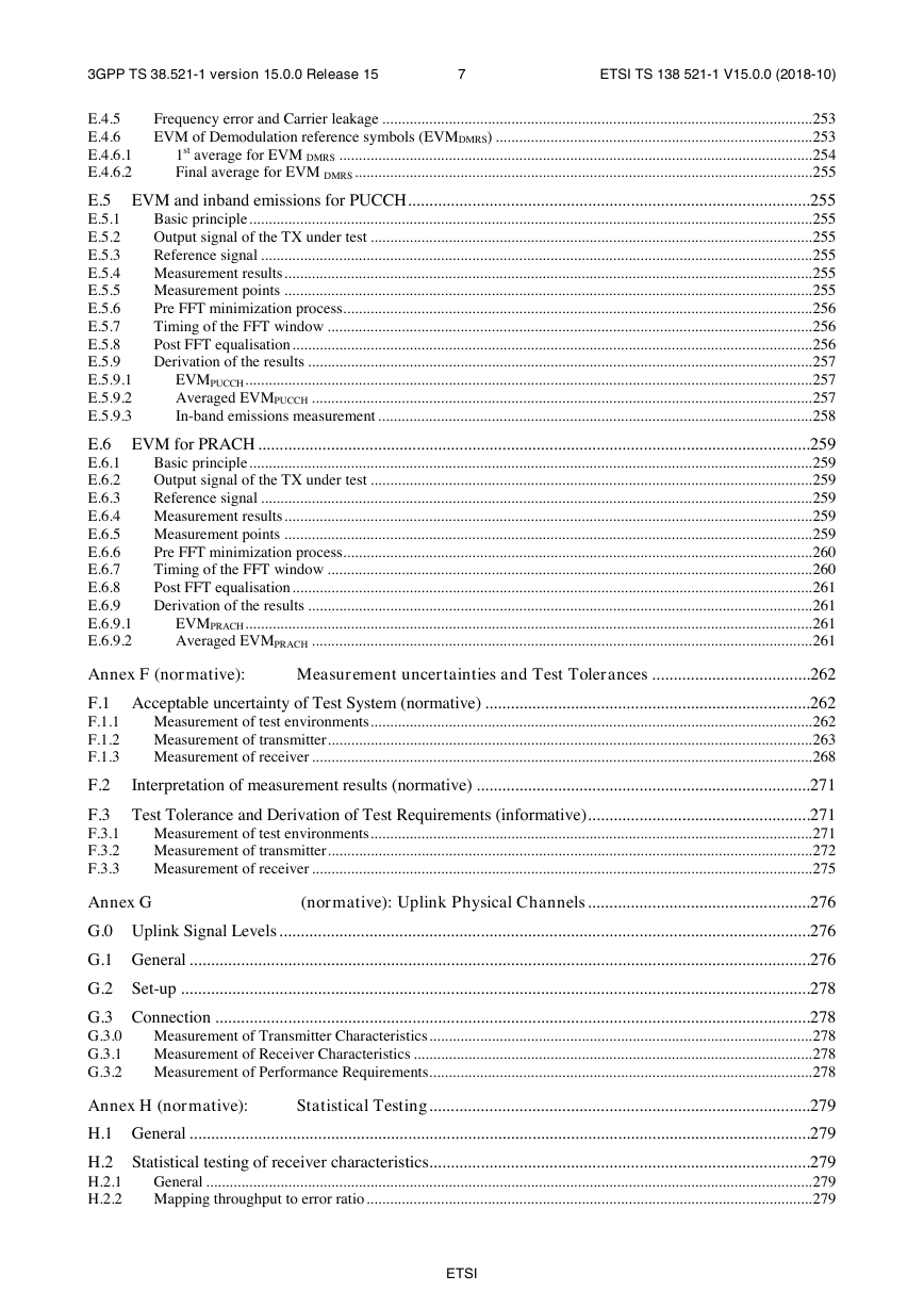
3GPP TS 38.521-1 version 15.0.0 Release 15 7 ETSI TS 138 521-1 V15.0.0 (2018-10) E.4.5 E.4.6 E.4.6.1 E.4.6.2 Frequency error and Carrier leakage .............................................................................................................. 253 EVM of Demodulation reference symbols (EVMDMRS) ................................................................................. 253 1st average for EVM DMRS ......................................................................................................................... 254 Final average for EVM DMRS ..................................................................................................................... 255 E.5 EVM and inband emissions for PUCCH .............................................................................................. 255 Basic principle ................................................................................................................................................ 255 E.5.1 Output signal of the TX under test ................................................................................................................. 255 E.5.2 Reference signal ............................................................................................................................................. 255 E.5.3 E.5.4 Measurement results ....................................................................................................................................... 255 Measurement points ....................................................................................................................................... 255 E.5.5 Pre FFT minimization process........................................................................................................................ 256 E.5.6 Timing of the FFT window ............................................................................................................................ 256 E.5.7 Post FFT equalisation ..................................................................................................................................... 256 E.5.8 E.5.9 Derivation of the results ................................................................................................................................. 257 EVMPUCCH ................................................................................................................................................. 257 E.5.9.1 Averaged EVMPUCCH ................................................................................................................................ 257 E.5.9.2 E.5.9.3 In-band emissions measurement ............................................................................................................... 258 E.6 EVM for PRACH ................................................................................................................................. 259 Basic principle ................................................................................................................................................ 259 E.6.1 Output signal of the TX under test ................................................................................................................. 259 E.6.2 Reference signal ............................................................................................................................................. 259 E.6.3 E.6.4 Measurement results ....................................................................................................................................... 259 Measurement points ....................................................................................................................................... 259 E.6.5 Pre FFT minimization process........................................................................................................................ 260 E.6.6 Timing of the FFT window ............................................................................................................................ 260 E.6.7 E.6.8 Post FFT equalisation ..................................................................................................................................... 261 Derivation of the results ................................................................................................................................. 261 E.6.9 EVMPRACH ................................................................................................................................................. 261 E.6.9.1 E.6.9.2 Averaged EVMPRACH ................................................................................................................................ 261 Annex F (normative): Measurement uncertainties and Test Tolerances ..................................... 262 F.1 Acceptable uncertainty of Test System (normative) ............................................................................ 262 Measurement of test environments ................................................................................................................. 262 F.1.1 F.1.2 Measurement of transmitter ............................................................................................................................ 263 Measurement of receiver ................................................................................................................................ 268 F.1.3 F.2 Interpretation of measurement results (normative) .............................................................................. 271 F.3 Test Tolerance and Derivation of Test Requirements (informative) .................................................... 271 F.3.1 Measurement of test environments ................................................................................................................. 271 Measurement of transmitter ............................................................................................................................ 272 F.3.2 F.3.3 Measurement of receiver ................................................................................................................................ 275 Annex G (normative): Uplink Physical Channels .................................................... 276 G.0 Uplink Signal Levels ............................................................................................................................ 276 G.1 General ................................................................................................................................................. 276 G.2 Set-up ................................................................................................................................................... 278 G.3 Connection ........................................................................................................................................... 278 Measurement of Transmitter Characteristics .................................................................................................. 278 G.3.0 G.3.1 Measurement of Receiver Characteristics ...................................................................................................... 278 Measurement of Performance Requirements.................................................................................................. 278 G.3.2 Annex H (normative): Statistical Testing ......................................................................................... 279 H.1 General ................................................................................................................................................. 279 H.2 Statistical testing of receiver characteristics......................................................................................... 279 General ........................................................................................................................................................... 279 H.2.1 H.2.2 Mapping throughput to error ratio .................................................................................................................. 279 ETSI
分享到:
收藏