logo资料库

H27Q1T8YEB9R-BCF_ Datasheet[26].pdf

第1页 / 共100页
第2页 / 共100页
第3页 / 共100页
第4页 / 共100页
第5页 / 共100页
第6页 / 共100页
第7页 / 共100页
第8页 / 共100页
资料共100页,剩余部分请下载后查看
Key features
1. SUMMARY DESCRIPTION
1.1. Product List
1.2. Part number Information
1.3. Definitions and Abbreviations
1.4. Diagram Legend
1.5. Block Diagram
Figure 1-1. NAND Flash Die Functional Block Diagram
2. Physical Interface and Measurement condition
2.1. Package Information
Figure 2-1. H27QDG8T2B8R, H27QDG8D2B8R: 1CE Single Channel ball assignments for 8-bit data sccess
Note 1) For H27QDG8D2B8R-BCF product, K-9 Pin site is a "Not Use".
Figure 2-2. H27QEG8UDB8R: 2CE Dual Channel ball assignments for 8-bit data sccess
(READ)Figure 2-3. H27QFG8VEB8R, H27Q1T8YEB9R & H27Q2T8CEB9R: 4CE Dual Channel ball assignments for 8-bit data sccess
Figure 2-4. TBD: 8CE Dual Channel ball assignments for 8-bit data sccess
Figure 2-5. BGA-152 ball spacing requrements (top & view, dimensions in millimeters)
Table 2-1. 152-fBGA 14x18mm, Package Mechanical Data
Figure 2-6. H27QFG8VQB2R, H27Q1T8YQB3R & H27Q2T8CEB3R: 4CE Quad-Channel, 316 ball assignments for 8- bit data sccess
Figure 2-7. BGA-316 ball spacing requrements (top & view, dimensions in millimeters)
Table 2-2. BGA-316 ball 14mmx18mm, Package Mechanical Data
2.2. PIN DESCRIPTION
Table 2-3. 152Ball fBGA Input/ Output capacitance (TA=25C, VCC=3.3V, f=100MHz)
Table 2-4. 316Ball fBGA Input/ Output capacitance (TA=25C, VCC=3.3V, f=100MHz)
2.3. Absolute Maximum DC Ratings
Table 2-5. Absolute maximum DC ratings
2.4. Operating temperature condition
Table 2-6. Operating Temperature Condition
2.5. Recommended Operating Conditions
Table 2-7. Recommended Operating Condition
2.6. AC Overshoot/Undershoot Requirements
Table 2-8. AC Overshoot/Undershoot Specification
Figure 2-8. Overshoot/Undershoot Diagram
2.7. DC and Operating Characteristics
Table 2-9. DC & Operating Characteristics for VccQ=3.3V (Single Die)
Table 2-10. DC & Operating Characteristics for VccQ=1.8V (Single Die)
2.8. AC Test Condition
Table 2-11. Single Ended without VREFQ AC & DC input level
Table 2-12. Single Ended with VREFQ AC & DC input level
Table 2-13. DC Electrical Characteristics for ODT (not supported)
2.8.1. VREFQ Tolerance
Figure 2-9. VREFQ(DC) tolerance and VREFQ AC-noise limits
2.8.2. Differential Input/Output AC Characteristics (VCCQ=1.8V only)
Table 2-14. Differential AC/DC Input Logic Level
Figure 2-10. Differential signal levels
2.8.3. DQ Driver Strength
Table 2-15. DQ Driver Strength Settings
Table 2-16. Testing Conditions for Impedance Values
Table 2-17. Output Driver Strength Impedance Values
Table 2-18. Pull-up and Pull-down Output Impedance Mismatch
2.8.4. Input/Output Slew rate
Table 2-19.Derating factor
Table 2-20.Input Slew rate
Table 2-21. Testing Conditions for Input Slew Rate
Table 2-22. Output Slew Rate Requirements
Table 2-23. Testing Conditions for Output Slew Rate
Figure 2-11. tRISE and tFALL Definition for Output Slew Rate
2.9. On-Die Termination (Not Supported)
2.9.1. On-Die Termination
2.9.2. ODT Setting
Figure 2-12. Set ODT Sequence
Figure 2-13. ODT Functional Representation
2.9.3. ODT On/Off During Read
2.9.4. ODT On/Off During Program
Figure 2-14. ODT On/Off During Program
2.10. AC and DC Input Measurement Levels
Table 2-24. AC Test condition
2.11. AC Timing Characteristics
2.11.1. Timing Parameters Description
Table 2-25. Toggle DDR Timing Parameters Description
2.11.2. Timing Parameters Table
Table 2-26. AC Timing Characteristics
2.11.3. Read/Program / Erase Characteristics
Table 2-27. NAND Read/Program/Erase Characteristics
3. Memory Organization
3.1. Memory Size
Figure 3-1. Memory organization for 128Gb Logical Unit
3.2. Addressing (I)
3.2.1. Single Die Addressing
Table 3-1. Memory addressing.
3.3. Target Memory Organization
Figure 3-2. Target Memory Organization
3.4. Addressing (II)
Figure 3-3. Row Address Layout
3.4.1. Plane Addressing
Figure 3-4. Position of Plane Address
3.4.2. Extended Block Arrangement
3.4.3. Valid Blocks
Table 3-2. The number of valid block
3. Invalid blocks are one that contains one or more bad bits. The device may contain bad blocks on shipment.
3.5. Factory Defect Mapping
3.5.1. Device Requirements
Figure 3-5. Area marked in first or last page of block indicating defect
3.5.2. Host Requirements
Figure 3-6. Flow chart to create initial invalid block table
3.6. Addressing For Program Operation
Table 3-2. Paired Page Address Information
4. FUNCTION DESCRIPTION
4.1. DATA PROTECTION AND POWER TRANSITION SEQUENCE
4.1.1. Data Protection
4.1.2. Power Up Sequence
4.1.3. Power Down Sequence
Figure 4-1. Initialization Timing
4.2. Data Interface / Timing Mode Transitions
4.2.1. The following transitions between data interface are supported:
4.2.2. SDR Transition from DDR
4.3. MLC to SLC mode transition (MLC2SLC)
4.3.1. Difference between MLC and SLC Addressing
Table 4-1. Memory SLC addressing.
Table 4-2. SLC Performance
4.4. Mode Selection
Table 4-3. Mode Selection
4.5. General Timing
4.5.1. Command Latch Cycle
Figure 4-3. Command Latch CycleI
4.5.2. Address Latch Cycle
Figure 4-4. Address Latch Cycle
4.5.3. Basic Data Input Timing
Figure 4-5. Basic Data Input Timing
4.5.4. Basic Data Output Timing
Figure 4-6. Basic Data Output Timing
4.5.5. Read ID Operation
Figure 4-7. Read ID Operation
4.5.6. Read Status Cycle
Figure 4-8. Read Status Cycle
4.5.6.1. Read Status cycle before Toggle DDR setting at Initialization sequence by FFh command
Figure 4-9. Read Status cycle before Toggle DDR setting at Initialization sequence by FFh command
4.5.7. Set Feature
Figure 4-10. Set Feature
4.5.8. Get Feature
Figure 4-11. Get Feature
4.5.9. Page Program Operation
Figure 4-12. Page Program Operation
5. Memory Operation
5.1. BASIC OPERATION
Basic Command sets
5.1.1. Page Read Operation
Figure 5-1. Page Read Sequence
5.1.1.1. Page Read Operation with Random Data Output
Figure 5-2. Page Read with Random Data Output Sequence
5.1.1.2. Data Out After Read Status
Figure 5-3. Data Out After Read Status Sequence
5.1.2. Fast 8KB Read (Fast Half page Read)
Figure 5-4. Fast Half READ sequence
Figure 5-5. Page layout for Fast Half READ
5.1.3. Page Program Operation
Figure 5-6. Page Program Sequence
5.1.3.1. Program Operation with Random Data Input
Figure 5-7. Program operation with Random Data Input Sequence
5.1.4. Block Erase Operation
Figure 5-8. Block Erase Sequence
5.1.5. Copy-Back Program Operation
Figure 5-9. Copy-Back Program Sequence
5.1.5.1. Copy-Back Program Operation with Random Data Input
Figure 5-10. Copy-Back Program with Random Data Input Sequence
5.1.6. Set Feature Operation
Figure 5-11. Set Feature Sequence
Table 5-1. Set feature addresses
5.1.6.1. Timing Mode setting (01h)
Table 5-2. Timing mode setting assignment
5.1.6.2. Toggle 2.0 specific setting (02h)
Table 5-3. Toggle 2.0 specific setting assignment
Table 5-4. Definition of Toggle 2.0 specific setting
Figure 5-12. Example of DQS latency (Write / Read)
5.1.6.3. Driver strength setting (10h)
Table 5-5. Definition of Driver strength setting
5.1.6.4. External VPP (30h)
5.1.7. Get Feature Operation
Figure 5-13. Get Feature Sequence
5.1.8. Read ID Operation
Figure 5-14. Read ID Sequence
5.1.8.1. 00h Address ID Definition
Table 5-7. 00h address ID cycle
Table 5-9. Read ID Definition - Address ID cycle
Table 5-10. 40h Address ID Cycle
Table 5-11. 40h Address ID Cycle
5.1.9. Read Status Operation
Table 5-12. Read Status Definition
Figure 5-15. Read Status Sequence
5.1.10. Reset Operation
Figure 5-16. Reset Sequence
5.1.11. Reset LUN operation
Figure 5-17. Single chip Reset Sequence
5.2. Extended OPERATION
5.2.1. Extended Command Sets
Table 5-13. Extended Command Sets
5.2.2. Two-Plane Page Read Operation
Figure 5-18. Example Timing with Two-plane Page Read (Primary)
Figure 5-19. Example Timing with Two-plane Page Read (Secondary)
5.2.3. Two-Plane Page Program Operation
Figure 5-20. Example Timing with Two-plane Page Program
5.2.4. Two-Plane Block Erase
Figure 5-21. Example Timing with Two-plane Block Erase
5.2.5. Two-Plane Copy-Back Program Operation
Figure 5-22. Example Timing with Two-plane Copy-Back Program (Primary)
Figure 5-23. Example Timing with Two-plane Copy-Back Program (Secondary)
5.2.6. Device Identification Table Read Operation
Figure 5-24. Device Identification Table Read Timing
5.2.7. Device Identification Table Definition
Table 5-14. Parameter Page Definitions
5.2.8. Read Status Enhanced
Table 5-15. Read Status Enhanced Definition
Figure 5-25 Read Status Sequence
5.2.11. Read LUN #0 Status Operation
Table 5-16. Read LUN#0 Status Definition
Figure 5-26. Read LUN#0 Sataus Sequence
5.2.12. Read LUN #1 Status Operation
Table 5-17. Read LUN#1 Status Definition
Figure 5-27. Read LUN#1 Sataus Sequence
5.2.13. Register Read Out Mode 1
Figure 5-28. Register Read Out
5.2.14. Two-Plane Register Read Out Mode 1
Figure 5-29. Two-Plane Register Read Out Mode 1
5.3. Interleaving Operation
5.3.1. Interleaving Page Program
Figure 5-30. Interleaving Page Program
5.3.2. Interleaving Page Read
Figure 5-31. Interleaving Page Read
5.3.3. Interleaving Block Erase
Figure 5-32. Interleaving Block Erase
5.3.4. Interleaving Two-Plane Page Program
Figure 5-33. Interleaving Two-Plane Page Program
5.3.5. Interleaving Two-Plane page Read
Figure 5-34. Interleaving Two-Plane page Read
5.3.6. Interleaving Multi-Plane Block Erase
Figure 5-35. Interleaving Multi-Plane Block Erase
5.3.7. Interleaving Read to Page Program
Figure 5-36. Interleaving Read to Page Program
5.3.8. Interleaving Copy-Back Program (1/2)
Figure 5-37. Interleaving Copy-Back Program (1/2)
5.3.9. Interleaving Copy-Back Program (2/2)
Figure 5-38. Interleaving Copy-Back Program (2/2)
5.3.10. Interleaving Two-Plane Copy Back Program(1/2)
Figure 5-39. Interleaving Two-Plane Copy Back Program(1/2)
5.3.11. Interleaving Two-Plane Copy Back Program(2/2)
Figure 5-40. Interleaving Two-Plane Copy Back Program(2/2)
5.4. Ready/Busy
Figure 5-41. Rp vs tr ,tf & Rp vs ibusy
Addendum
1. Command Description
1.1. Set Parameter
1.1.1. Command Sequence
1.1.2. Timing Diagram
Figure 1. Set Parameter for SDR
Figure 2. Set Parameter for NV-DDR2
1.1.3. Rules and Limitations
1.2. Get Parameter
1.2.1. Command Sequence
Figure 3. Get Parameter for SDR
Figure 4. Get Parameter for NV-DDR2
1.2.3. Rules and Limitations
128Gb Based NAND Flash 128Gb, 256Gb, 512Gb, 1Tb and 2Tb NAND Flash Specification Rev_1.9 /Jun. 2015 1
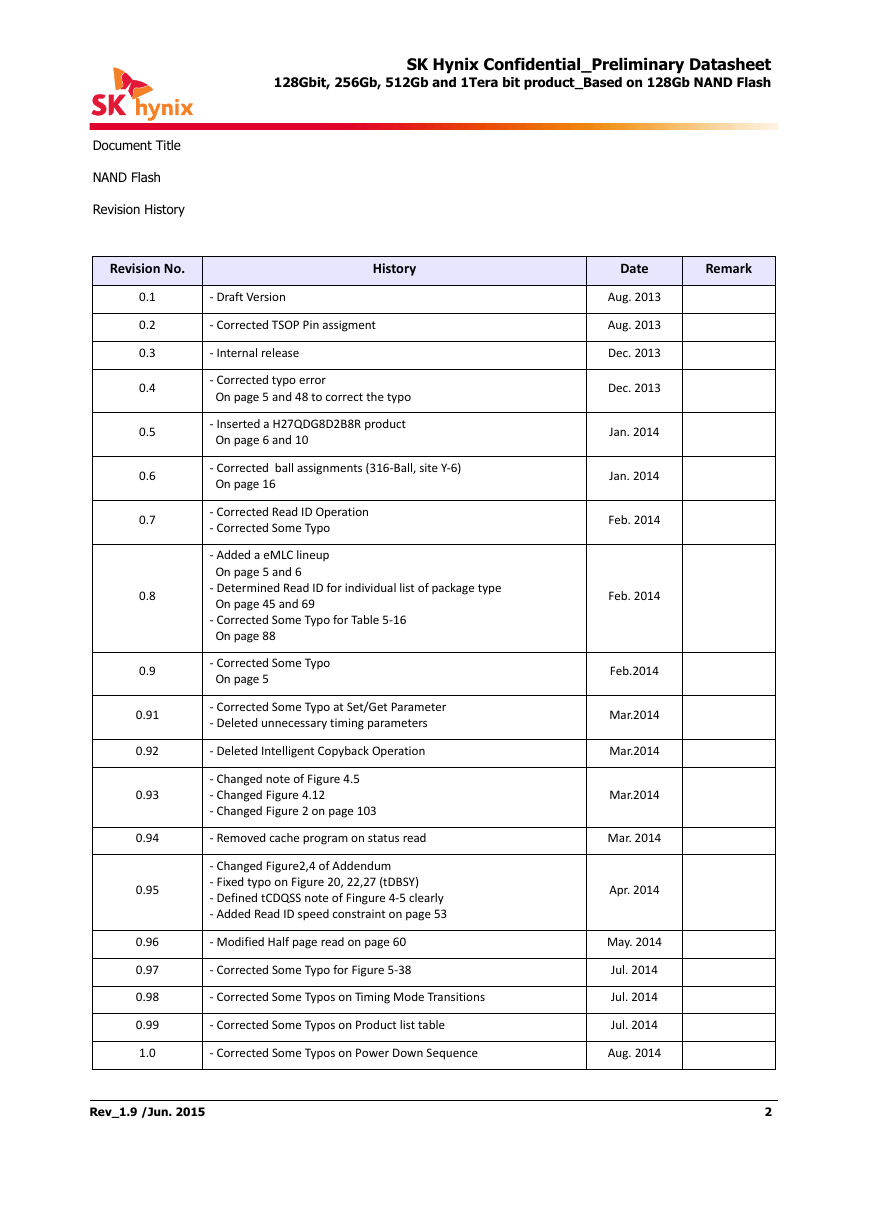
SK Hynix Confidential_Preliminary Datasheet 128Gbit, 256Gb, 512Gb and 1Tera bit product_Based on 128Gb NAND Flash Document Title NAND Flash Revision History Revision No. History Date Remark 0.1 0.2 0.3 0.4 0.5 0.6 0.7 0.8 0.9 0.91 0.92 0.93 0.94 0.95 0.96 0.97 0.98 0.99 1.0 - Draft Version - Corrected TSOP Pin assigment - Internal release - Corrected typo error On page 5 and 48 to correct the typo - Inserted a H27QDG8D2B8R product On page 6 and 10 - Corrected ball assignments (316-Ball, site Y-6) On page 16 - Corrected Read ID Operation - Corrected Some Typo - Added a eMLC lineup On page 5 and 6 - Determined Read ID for individual list of package type On page 45 and 69 - Corrected Some Typo for Table 5-16 On page 88 - Corrected Some Typo On page 5 - Corrected Some Typo at Set/Get Parameter - Deleted unnecessary timing parameters - Deleted Intelligent Copyback Operation - Changed note of Figure 4.5 - Changed Figure 4.12 - Changed Figure 2 on page 103 - Removed cache program on status read - Changed Figure2,4 of Addendum - Fixed typo on Figure 20, 22,27 (tDBSY) - Defined tCDQSS note of Fingure 4-5 clearly - Added Read ID speed constraint on page 53 - Modified Half page read on page 60 - Corrected Some Typo for Figure 5-38 - Corrected Some Typos on Timing Mode Transitions - Corrected Some Typos on Product list table - Corrected Some Typos on Power Down Sequence Aug. 2013 Aug. 2013 Dec. 2013 Dec. 2013 Jan. 2014 Jan. 2014 Feb. 2014 Feb. 2014 Feb.2014 Mar.2014 Mar.2014 Mar.2014 Mar. 2014 Apr. 2014 May. 2014 Jul. 2014 Jul. 2014 Jul. 2014 Aug. 2014 Rev_1.9 /Jun. 2015 2
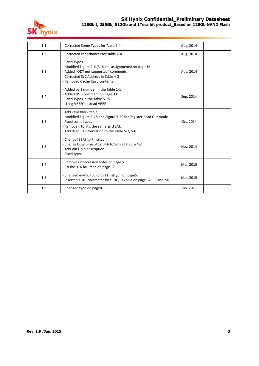
SK Hynix Confidential_Preliminary Datasheet 128Gbit, 256Gb, 512Gb and 1Tera bit product_Based on 128Gb NAND Flash 1.1 1.2 1.3 1.4 1.5 1.6 1.7 1.8 1.9 - Corrected Some Typos for Table 2-4 - Corrected capacitances for Table 2-4 - Fixed Typos - Modified Figure 2-6 (316 ball assignments) on page 16 - Added “ODT not supported” comments - Corrected SLC Address in Table 4-3 - Removed Cache Read contents - Added part number in the Table 1-1 - Added tWB comment on page 33 - Fixed Typos in the Table 5-15 - Using VREFQ instead VREF - Add valid block table - Modified Figure 5-28 and Figure 5-29 for Register Read Out mode - Fixed some typos - Remove tITC, it’s the same as tFEAT. - Add Read ID information to the Table 5-7, 5-8 - Change tBERS to 7ms(typ.) - Change busy time of 1st FFh to 5ms at Figure 4-2 - Add VREF pin description - Fixed typos - Remove unnecessary notes on page 5 - Fix the 316 ball map on page 17 - Changed e-MLC tBERS to 11ms(typ.) on page5 - Inserted a AC parameter for tCDQSH value on page 32, 33 and 56. - Changed typo on page8 Aug. 2014 Aug. 2014 Aug. 2014 Sep. 2014 Oct. 2014 Nov. 2014 Mar. 2015 Mar. 2015 Jun. 2015 Rev_1.9 /Jun. 2015 3
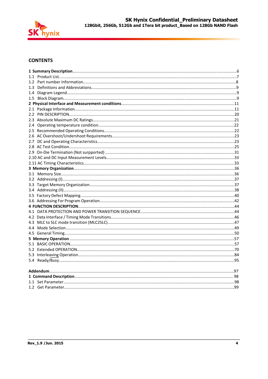
SK Hynix Confidential_Preliminary Datasheet 128Gbit, 256Gb, 512Gb and 1Tera bit product_Based on 128Gb NAND Flash CONTENTS 1 Summary Description.................................................................................................................................................6 1.1 Product List.............................................................................................................................................................7 1.2 Part number Information.......................................................................................................................................8 1.3 Definitions and Abbreviations................................................................................................................................9 1.4 Diagram Legend......................................................................................................................................................9 1.5 Block Diagram.........................................................................................................................................................9 2 Physical Interface and Measurement conditions....................................................................................................11 2.1 Package Information.............................................................................................................................................11 2.2 PIN DESCRIPTION..................................................................................................................................................20 2.3 Absolute Maximum DC Ratings.............................................................................................................................21 2.4 Operating temperature condition........................................................................................................................22 2.5 Recommended Operating Conditions...................................................................................................................22 2.6 AC Overshoot/Undershoot Requirements............................................................................................................23 2.7 DC and Operating Characteristics.........................................................................................................................23 2.8 AC Test Condition..................................................................................................................................................25 2.9 On-Die Termination (Not surpported) ..................................................................................................................31 2.10 AC and DC Input Measurement Levels.................................................................................................................33 2.11 AC Timing Characteristics.....................................................................................................................................33 3 Memory Organization..............................................................................................................................................36 3.1 Memory Size.........................................................................................................................................................36 3.2 Addressing (I)........................................................................................................................................................37 3.3 Target Memory Organization................................................................................................................................37 3.4 Addressing (II).......................................................................................................................................................38 3.5 Factory Defect Mapping........................................................................................................................................40 3.6 Addressing For Program Operation.......................................................................................................................42 4 FUNCTION DESCRIPTION..........................................................................................................................................44 4.1 DATA PROTECTION AND POWER TRANSITION SEQUENCE...................................................................................44 4.2 Data Interface / Timing Mode Transitions.............................................................................................................46 4.3 MLC to SLC mode transition (MLC2SLC)................................................................................................................47 4.4 Mode Selection.....................................................................................................................................................49 4.5 General Timing......................................................................................................................................................50 5 Memory Operation..................................................................................................................................................57 5.1 BASIC OPERATION.................................................................................................................................................57 5.2 Extended OPERATION...........................................................................................................................................70 5.3 Interleaving Operation..........................................................................................................................................84 5.4 Ready/Busy...........................................................................................................................................................95 Addendum...................................................................................................................................................................97 1 Command Description............................................................................................................................................ 98 1.1 Set Parameter.......................................................................................................................................................98 1.2 Get Parameter......................................................................................................................................................99 Rev_1.9 /Jun. 2015 4
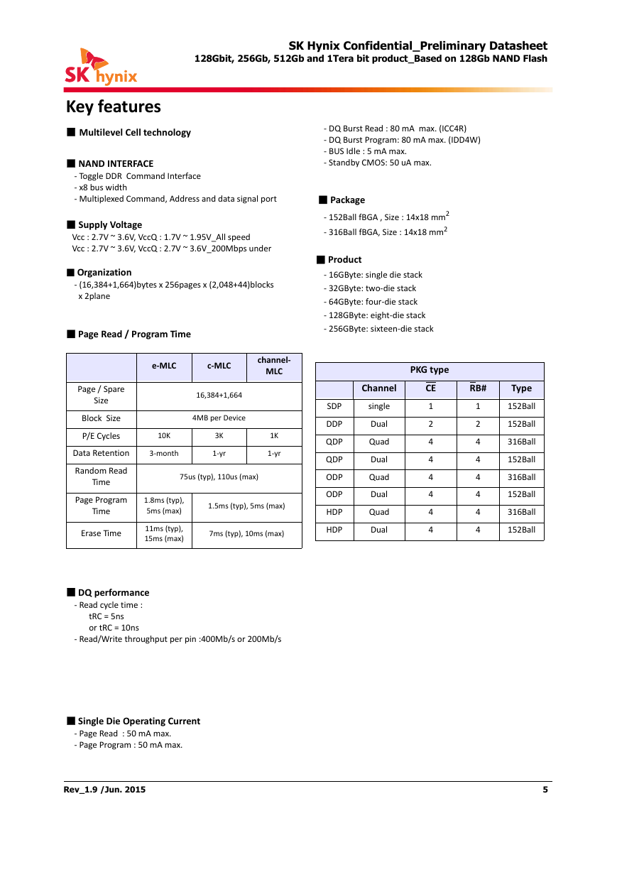
SK Hynix Confidential_Preliminary Datasheet 128Gbit, 256Gb, 512Gb and 1Tera bit product_Based on 128Gb NAND Flash - DQ Burst Read : 80 mA max. (ICC4R) - DQ Burst Program: 80 mA max. (IDD4W) - BUS Idle : 5 mA max. - Standby CMOS: 50 uA max. ■ Package - 152Ball fBGA , Size : 14x18 mm2 - 316Ball fBGA, Size : 14x18 mm2 ■ Product - 16GByte: single die stack - 32GByte: two-die stack - 64GByte: four-die stack - 128GByte: eight-die stack - 256GByte: sixteen-die stack PKG type Channel single Dual Quad Dual Quad Dual Quad Dual SDP DDP QDP QDP ODP ODP HDP HDP CE 1 2 4 4 4 4 4 4 RB# 1 2 4 4 4 4 4 4 Type 152Ball 152Ball 316Ball 152Ball 316Ball 152Ball 316Ball 152Ball Key features ■ Multilevel Cell technology ■ NAND INTERFACE - Toggle DDR Command Interface - x8 bus width - Multiplexed Command, Address and data signal port ■ Supply Voltage Vcc : 2.7V ~ 3.6V, VccQ : 1.7V ~ 1.95V_All speed Vcc : 2.7V ~ 3.6V, VccQ : 2.7V ~ 3.6V_200Mbps under ■ Organization - (16,384+1,664)bytes x 256pages x (2,048+44)blocks x 2plane ■ Page Read / Program Time e-MLC c-MLC channel- MLC 16,384+1,664 4MB per Device 10K 3-month 3K 1-yr 1K 1-yr 75us (typ), 110us (max) 1.8ms (typ), 5ms (max) 11ms (typ), 15ms (max) 1.5ms (typ), 5ms (max) 7ms (typ), 10ms (max) Page / Spare Size Block Size P/E Cycles Data Retention Random Read Time Page Program Time Erase Time ■ DQ performance - Read cycle time : tRC = 5ns or tRC = 10ns - Read/Write throughput per pin :400Mb/s or 200Mb/s ■ Single Die Operating Current - Page Read : 50 mA max. - Page Program : 50 mA max. Rev_1.9 /Jun. 2015 5
SK Hynix Confidential_Preliminary Datasheet 128Gbit, 256Gb, 512Gb and 1Tera bit product_Based on 128Gb NAND Flash 1. SUMMARY DESCRIPTION The SKHynix NAND Flash is suited for high performance applications which use the batteries such as high-end mobile solution and PCs data storage solution. The 128Gb based NAND series has a toggle DDR interface. Operates from a bidirectional DQS : SKHynix NAND Flash technology provides high-performance NAND Flash memory with an interface that supports up to 200Mbps or up to 400Mbps data read and write throughput. H27Uxx8xxBxR-BCF NAND Flash has a fast interface, rated at 200Mbps, as compared to 40Mbps for legacy single data rate. H27Qxx8xxBxR-BCC NAND Flash relatively already 40Mbps of speed of information processing of SDR NAND Flash are 10 times faster, amount to 400Mbps. The high-speed bandwidth of SKHynix NAND Flash is supported to better support the ongoing shift toward advanced interfaces, as more mobile and PCs electronics devices requiring added performance and higher densities adopt interfaces such as embed- ded NAND solution series and Serial SSD solution series. Rev_1.9 /Jun. 2015 6
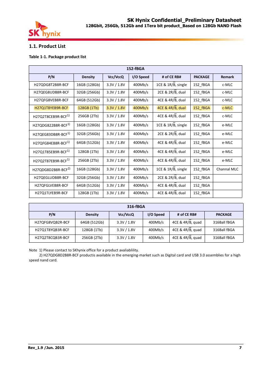
SK Hynix Confidential_Preliminary Datasheet 128Gbit, 256Gb, 512Gb and 1Tera bit product_Based on 128Gb NAND Flash 1.1. Product List Table 1-1. Package product list 152-fBGA P/N H27QDG8T2B8R-BCF H27QEG8UDB8R-BCF H27QFG8VEB8R-BCF H27Q1T8YEB9R-BCF H27Q2T8CEB9R-BCF1) H27QDG822B8R-BCF1) H27QEG83DB8R-BCF1) H27QFG84EB8R-BCF1) H27Q1T85EB9R-BCF1) H27Q2T87EB9R-BCF1) H27QDG8D2B8R-BCF2) H27QEGLUDB8R-BCF H27QFGLVEB8R-BCF H27Q1TLYEB9R-BCF Density 16GB (128Gb) 32GB (256Gb) 64GB (512Gb) 128GB (1Tb) Vcc/VccQ 3.3V / 1.8V 3.3V / 1.8V 3.3V / 1.8V 3.3V / 1.8V I/O Speed 400Mb/s 400Mb/s 400Mb/s 400Mb/s # of CE RB# 1CE & 1R/B, single 2CE & 2R/B, dual 4CE & 4R/B, dual 4CE & 4R/B, dual PACKAGE 152_fBGA 152_fBGA 152_fBGA 152_fBGA 256GB (2Tb) 3.3V / 1.8V 400Mb/s 4CE & 4R/B, dual 152_fBGA 16GB (128Gb) 3.3V / 1.8V 400Mb/s 1CE & 1R/B, single 152_fBGA 32GB (256Gb) 3.3V / 1.8V 400Mb/s 2CE & 2R/B, dual 152_fBGA 64GB (512Gb) 3.3V / 1.8V 400Mb/s 4CE & 4R/B, dual 152_fBGA 128GB (1Tb) 3.3V / 1.8V 400Mb/s 4CE & 4R/B, dual 152_fBGA 256GB (2Tb) 3.3V / 1.8V 400Mb/s 4CE & 4R/B, dual 152_fBGA Remark c-MLC c-MLC c-MLC c-MLC c-MLC e-MLC e-MLC e-MLC e-MLC e-MLC 16GB (128Gb) 3.3V / 1.8V 400Mb/s 1CE & 1R/B, single 152_fBGA Channal MLC 32GB (256Gb) 64GB (512Gb) 128GB (1Tb) 3.3V / 1.8V 3.3V / 1.8V 3.3V / 1.8V 400Mb/s 400Mb/s 400Mb/s 2CE & 2R/B, dual 4CE & 4R/B, dual 4CE & 4R/B, dual 152_fBGA 152_fBGA 152_fBGA 316-fBGA P/N H27QFG8VQB2R-BCF H27Q1T8YQB3R-BCF H27Q2T8CQB3R-BCF Density 64GB (512Gb) 128GB (1Tb) 256GB (2Tb) Vcc/VccQ 3.3V / 1.8V 3.3V / 1.8V 3.3V / 1.8V I/O Speed 400Mb/s 400Mb/s 400Mb/s # of CE RB# 4CE & 4R/B, quad 4CE & 4R/B, quad 4CE & 4R/B, quad PACKAGE 316Ball fBGA 316Ball fBGA 316Ball fBGA Note 1) Please contact to SKhynix office for a product avaliablility. 2) H27QDG8D2B8R-BCF productis available in the emerging-market such as Digital card and USB 3.0 assemblies for a high speed nand card. Rev_1.9 /Jun. 2015 7
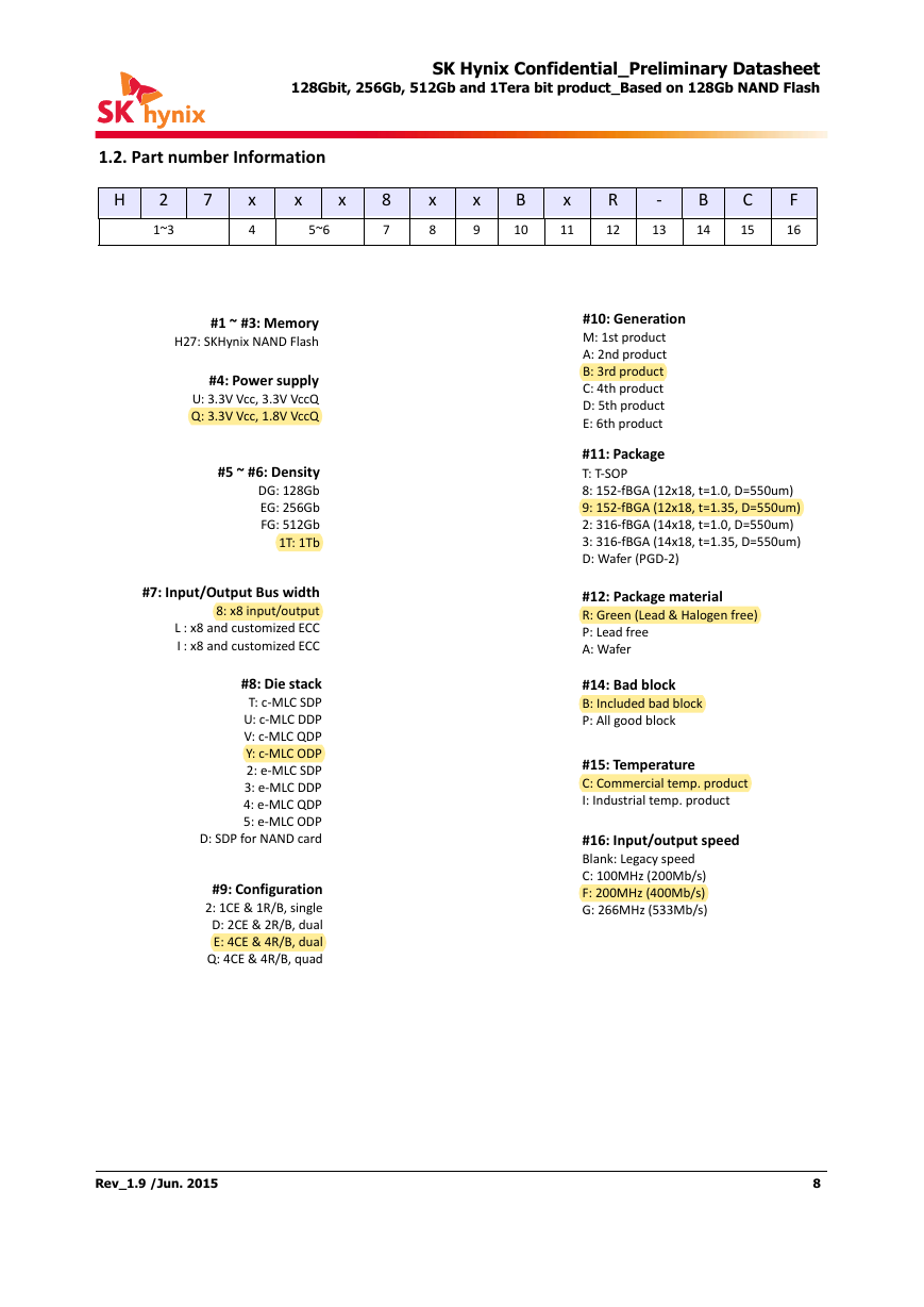
SK Hynix Confidential_Preliminary Datasheet 128Gbit, 256Gb, 512Gb and 1Tera bit product_Based on 128Gb NAND Flash 1.2. Part number Information H 7 2 1~3 x 4 x x 5~6 8 7 x 8 x 9 B 10 x 11 R 12 - 13 B 14 C 15 F 16 #1 ~ #3: Memory H27: SKHynix NAND Flash #4: Power supply U: 3.3V Vcc, 3.3V VccQ Q: 3.3V Vcc, 1.8V VccQ #5 ~ #6: Density DG: 128Gb EG: 256Gb FG: 512Gb 1T: 1Tb #7: Input/Output Bus width 8: x8 input/output L : x8 and customized ECC I : x8 and customized ECC #8: Die stack T: c-MLC SDP U: c-MLC DDP V: c-MLC QDP Y: c-MLC ODP 2: e-MLC SDP 3: e-MLC DDP 4: e-MLC QDP 5: e-MLC ODP D: SDP for NAND card #9: Configuration 2: 1CE & 1R/B, single D: 2CE & 2R/B, dual E: 4CE & 4R/B, dual Q: 4CE & 4R/B, quad #10: Generation M: 1st product A: 2nd product B: 3rd product C: 4th product D: 5th product E: 6th product #11: Package T: T-SOP 8: 152-fBGA (12x18, t=1.0, D=550um) 9: 152-fBGA (12x18, t=1.35, D=550um) 2: 316-fBGA (14x18, t=1.0, D=550um) 3: 316-fBGA (14x18, t=1.35, D=550um) D: Wafer (PGD-2) #12: Package material R: Green (Lead & Halogen free) P: Lead free A: Wafer #14: Bad block B: Included bad block P: All good block #15: Temperature C: Commercial temp. product I: Industrial temp. product #16: Input/output speed Blank: Legacy speed C: 100MHz (200Mb/s) F: 200MHz (400Mb/s) G: 266MHz (533Mb/s) Rev_1.9 /Jun. 2015 8
分享到:
收藏