�
Source: Phase-Locked Loops
Chapter
1
Introduction to PLLs
1.1 Operating Principles of the PLL
The phase-locked loop (PLL) helps keep parts of our world orderly. If we turn
on a television set, a PLL will keep heads at the top of the screen and feet at
the bottom. In color television, another PLL makes sure that green remains
green and red remains red (even if the politicians claim that the reverse is true).
A PLL is a circuit that causes a particular system to track with another one.
More precisely, a PLL is a circuit synchronizing an output signal (generated by
an oscillator) with a reference or input signal in frequency as well as in phase.
In the synchronized—often called locked—state the phase error between the
oscillator’s output signal and the reference signal is zero, or remains constant.
If a phase error builds up, a control mechanism acts on the oscillator in such
a way that the phase error is again reduced to a minimum. In such a control
system the phase of the output signal is actually locked to the phase of the ref-
erence signal. This is why it is referred to as a phase-locked loop.
The operating principle of the PLL is explained by the example of the linear
PLL (LPLL). As will be pointed out in Sec. 1.2, there exist other types of PLLs,
e.g., digital PLLs (DPLLs), all-digital PLLs (ADPLLs), and software PLLs
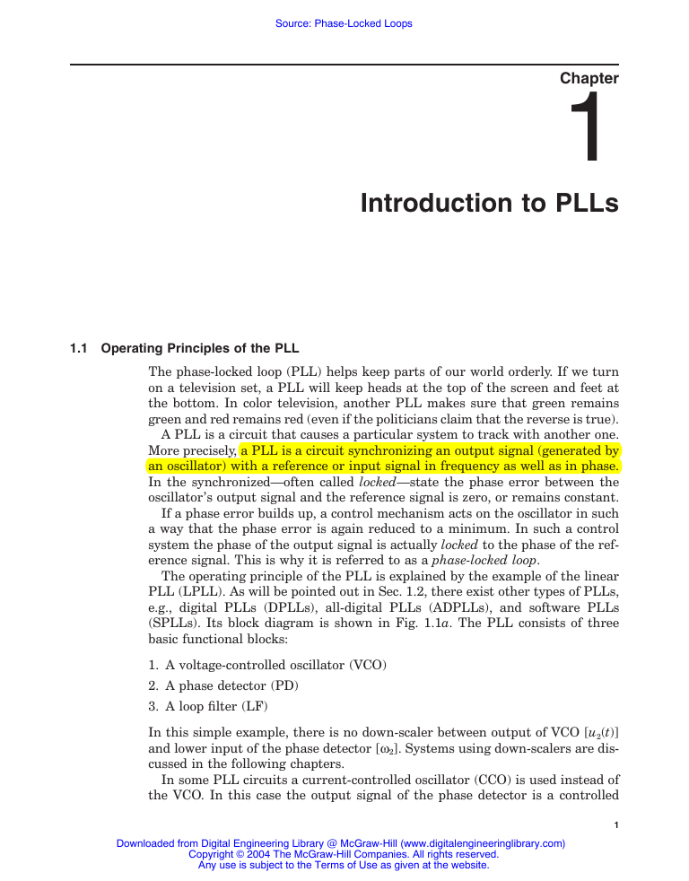
(SPLLs). Its block diagram is shown in Fig. 1.1a. The PLL consists of three
basic functional blocks:
1. A voltage-controlled oscillator (VCO)
2. A phase detector (PD)
3. A loop filter (LF)
In this simple example, there is no down-scaler between output of VCO [u2(t)]
and lower input of the phase detector [w2]. Systems using down-scalers are dis-
cussed in the following chapters.
In some PLL circuits a current-controlled oscillator (CCO) is used instead of
the VCO. In this case the output signal of the phase detector is a controlled
1
Downloaded from Digital Engineering Library @ McGraw-Hill (www.digitalengineeringlibrary.com)
Copyright © 2004 The McGraw-Hill Companies. All rights reserved.
Any use is subject to the Terms of Use as given at the website.
Introduction to PLLs
2
Chapter One
input
signal u1 (t) (w1)
(w2)
ud(t)
uf (t) FM-output
phase detector
loop filter
output signal u2(t)
voltage controlled
oscillator
(a)
w2
wo
(b)
uf
ud
(c)
qe
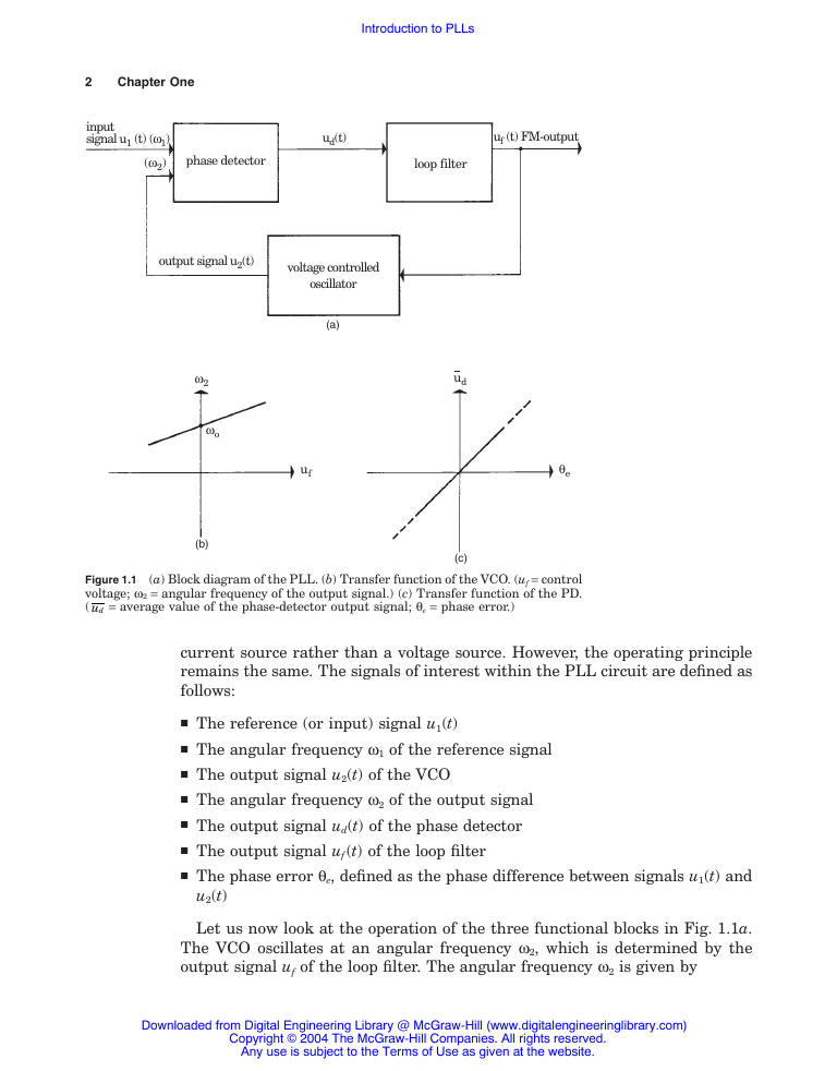
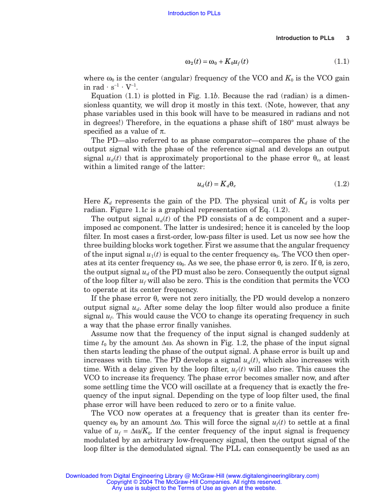
Figure 1.1 (a) Block diagram of the PLL. (b) Transfer function of the VCO. (uf = control
voltage; w2 = angular frequency of the output signal.) (c) Transfer function of the PD.
ud
(
= average value of the phase-detector output signal; qe = phase error.)
current source rather than a voltage source. However, the operating principle
remains the same. The signals of interest within the PLL circuit are defined as
follows:
䊏 The reference (or input) signal u1(t)
䊏 The angular frequency w1 of the reference signal
䊏 The output signal u2(t) of the VCO
䊏 The angular frequency w2 of the output signal
䊏 The output signal ud(t) of the phase detector
䊏 The output signal uf(t) of the loop filter
䊏 The phase error qe, defined as the phase difference between signals u1(t) and
u2(t)
Let us now look at the operation of the three functional blocks in Fig. 1.1a.
The VCO oscillates at an angular frequency w2, which is determined by the
output signal uf of the loop filter. The angular frequency w2 is given by
Downloaded from Digital Engineering Library @ McGraw-Hill (www.digitalengineeringlibrary.com)
Copyright © 2004 The McGraw-Hill Companies. All rights reserved.
Any use is subject to the Terms of Use as given at the website.
�
Introduction to PLLs
Introduction to PLLs
3
w
( ) =
t
w
+
( )
K u tf
0
0
2
(1.1)
where w0 is the center (angular) frequency of the VCO and K0 is the VCO gain
in rad · s-1 · V-1.
Equation (1.1) is plotted in Fig. 1.1b. Because the rad (radian) is a dimen-
sionless quantity, we will drop it mostly in this text. (Note, however, that any
phase variables used in this book will have to be measured in radians and not
in degrees!) Therefore, in the equations a phase shift of 180° must always be
specified as a value of p.
The PD—also referred to as phase comparator—compares the phase of the
output signal with the phase of the reference signal and develops an output
signal ud(t) that is approximately proportional to the phase error qe, at least
within a limited range of the latter:
u t K
d
( ) =
q
d e
(1.2)
Here Kd represents the gain of the PD. The physical unit of Kd is volts per
radian. Figure 1.1c is a graphical representation of Eq. (1.2).
The output signal ud(t) of the PD consists of a dc component and a super-
imposed ac component. The latter is undesired; hence it is canceled by the loop
filter. In most cases a first-order, low-pass filter is used. Let us now see how the
three building blocks work together. First we assume that the angular frequency
of the input signal u1(t) is equal to the center frequency w0. The VCO then oper-
ates at its center frequency w0. As we see, the phase error qe is zero. If qe is zero,
the output signal ud of the PD must also be zero. Consequently the output signal
of the loop filter uf will also be zero. This is the condition that permits the VCO
to operate at its center frequency.
If the phase error qe were not zero initially, the PD would develop a nonzero
output signal ud. After some delay the loop filter would also produce a finite
signal uf. This would cause the VCO to change its operating frequency in such
a way that the phase error finally vanishes.
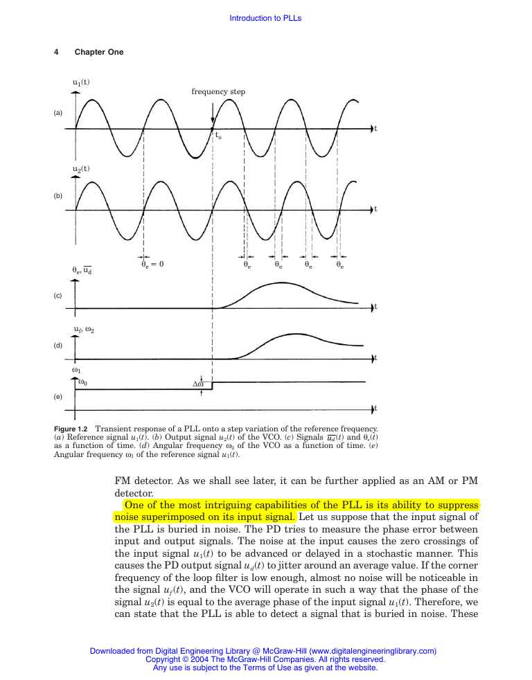
Assume now that the frequency of the input signal is changed suddenly at
time t0 by the amount Dw. As shown in Fig. 1.2, the phase of the input signal
then starts leading the phase of the output signal. A phase error is built up and
increases with time. The PD develops a signal ud(t), which also increases with
time. With a delay given by the loop filter, uf(t) will also rise. This causes the
VCO to increase its frequency. The phase error becomes smaller now, and after
some settling time the VCO will oscillate at a frequency that is exactly the fre-
quency of the input signal. Depending on the type of loop filter used, the final
phase error will have been reduced to zero or to a finite value.
The VCO now operates at a frequency that is greater than its center fre-
quency w0 by an amount Dw. This will force the signal uf(t) to settle at a final
value of uf = Dw/K0. If the center frequency of the input signal is frequency
modulated by an arbitrary low-frequency signal, then the output signal of the
loop filter is the demodulated signal. The PLL can consequently be used as an
Downloaded from Digital Engineering Library @ McGraw-Hill (www.digitalengineeringlibrary.com)
Copyright © 2004 The McGraw-Hill Companies. All rights reserved.
Any use is subject to the Terms of Use as given at the website.
�
Introduction to PLLs
4
Chapter One
u1(t)
u2(t)
qe, ud
uf, w2
w1
w0
(a)
(b)
(c)
(d)
(e)
frequency step
to
qe = 0
qe
qe
qe
qe
Dw
t
t
t
t
t
Figure 1.2 Transient response of a PLL onto a step variation of the reference frequency.
(t) and qe(t)
(a) Reference signal u1(t). (b) Output signal u2(t) of the VCO. (c) Signals
as a function of time. (d) Angular frequency w2 of the VCO as a function of time. (e)
Angular frequency w1 of the reference signal u1(t).
ud
FM detector. As we shall see later, it can be further applied as an AM or PM
detector.
One of the most intriguing capabilities of the PLL is its ability to suppress
noise superimposed on its input signal. Let us suppose that the input signal of
the PLL is buried in noise. The PD tries to measure the phase error between
input and output signals. The noise at the input causes the zero crossings of
the input signal u1(t) to be advanced or delayed in a stochastic manner. This
causes the PD output signal ud(t) to jitter around an average value. If the corner
frequency of the loop filter is low enough, almost no noise will be noticeable in
the signal uf(t), and the VCO will operate in such a way that the phase of the
signal u2(t) is equal to the average phase of the input signal u1(t). Therefore, we
can state that the PLL is able to detect a signal that is buried in noise. These
Downloaded from Digital Engineering Library @ McGraw-Hill (www.digitalengineeringlibrary.com)
Copyright © 2004 The McGraw-Hill Companies. All rights reserved.
Any use is subject to the Terms of Use as given at the website.
�
Introduction to PLLs
Introduction to PLLs
5
simplified considerations have shown that the PLL is nothing but a servo
system that controls the phase of the output signal u2(t).
As shown in Fig. 1.2, the PLL was always able to track the phase of the output
signal to the phase of the reference signal; this system was locked at all times.
This is not necessarily the case, however, because a larger frequency step
applied to the input signal could cause the system to ‘‘unlock.’’ The control
mechanism inherent in the PLL will then try to become locked again, but will
the system indeed lock again? We shall deal with this problem in the following
chapters. Basically two kinds of problems have to be considered:
䊏 The PLL is initially locked. Under what conditions will the PLL remain
locked?
䊏 The PLL is initially unlocked. Under what conditions will the PLL become
locked?
If we try to answer these questions, we notice that different PLLs behave quite
differently in this regard. We find that there are some fundamentally different
types of PLLs. Therefore, we first identify these various types.
1.2 Classification of PLL Types
The very first phase-locked loops (PLLs) were implemented as early as 1932 by
de Bellescize22; this French engineer is considered the inventor of “coherent
communication.” The PLL found broader industrial applications only when it
became available as an integrated circuit. The first PLL ICs appeared around
1965 and were purely analog devices. An analog multiplier (four-quadrant mul-
tiplier) was used as the phase detector, the loop filter was built from a passive
or active RC filter, and the well-known voltage-controlled oscillator (VCO) was
used to generate the output signal of the PLL. This type of PLL is referred to
as the “linear PLL” (LPLL) today. In the following years the PLL drifted slowly
but steadily into digital territory. The very first digital PLL (DPLL), which
appeared around 1970, was in effect a hybrid device: only the phase detector
was built from a digital circuit, e.g., from an EXOR gate or a JK-flipflop, but
the remaining blocks were still analog. A few years later, the “all-digital” PLL
(ADPLL) was invented. The ADPLL is exclusively built from digital func-
tion blocks and hence doesn’t contain any passive components like resistors and
capacitors.
Analogous to filters, PLLs can also be implemented by software. In this case,
the function of the PLL is no longer performed by a piece of specialized hard-
ware, but rather by a computer program. This last type of PLL is referred to
as SPLL.
Different types of PLLs behave differently, so there is no common theory that
covers all kinds of PLLs. The performance of LPLLs and DPLLs is similar,
however; hence we can develop a theory that is valid for both categories. We
will deal with LPLLs and DPLLs in Chap. 2, “Mixed-Signal PLLs.” The term
Downloaded from Digital Engineering Library @ McGraw-Hill (www.digitalengineeringlibrary.com)
Copyright © 2004 The McGraw-Hill Companies. All rights reserved.
Any use is subject to the Terms of Use as given at the website.
�
Introduction to PLLs
6
Chapter One
“mixed” indicates that these PLLs are mostly hybrids built from linear and
digital circuits. Strictly speaking, only the DPLL is a mixed-signal circuit; the
LPLL is purely analog. The ADPLL behaves very differently from mixed-signal
PLLs and hence is treated in a separate chapter (Chap. 6).
The software PLL is normally implemented by a hardware platform such as
a microcontroller or a digital signal processor (DSP). The PLL function is real-
ized by software. This offers the greatest flexibility, because a vast number of
different algorithms can be developed. For example, an SPLL can be pro-
grammed to behave like an LPLL, a DPLL, or an ADPLL. We will deal with
SPLLs in Chap. 8.
Downloaded from Digital Engineering Library @ McGraw-Hill (www.digitalengineeringlibrary.com)
Copyright © 2004 The McGraw-Hill Companies. All rights reserved.
Any use is subject to the Terms of Use as given at the website.
�
Source: Phase-Locked Loops
Chapter
2
Mixed-Signal PLLs
2.1 Block Diagram of the Mixed-Signal PLL
As mentioned in Sec. 1.2, the mixed-signal PLL includes circuits that are
hybrids of both linear and digital circuits. To see which parts of the system are
linear and which are digital, we consider the general block diagram in Fig. 2.1.
As shown in Sec. 1.1 every PLL consists of the three blocks: phase detector, loop
filter, and voltage-controlled oscillator (VCO). When the PLL is used as a fre-
quency synthesizer, another block is added: a divide-by-N counter. Assuming
that the counter divides by a factor N, the frequency of the VCO output signal
is forced then to be N times the reference frequency (the frequency of the input
signal u1). In most cases the divider ratio N is made programmable. We will deal
extensively with frequency synthesizers in Chap. 3.
When a down-scaler is inserted, the term center frequency becomes ambigu-
ous: the center (radian) frequency w0 can be related to the output of the VCO
(as done in Sec. 1.1), but it could also be related to the output of the down-
scaler, or in other words, to the input of the PLL. To remove this dilemma, we
introduce two different terms for center (radian) frequency: we will use the
symbol w0 to denote the center frequency at the output of the VCO, and the
symbol w0¢ to denote the center radian frequency at the input of the PLL. Obvi-
ously, w0 and w0¢ are related by w0¢ = w0/N. As seen from Fig. 2.1, the quantities
related to the output signal of the down-scaler are characterized by a prime
(¢ symbol), e.g., u2¢, w2¢. When the VCO does not operate at its center frequency
(uf π 0), its output radian frequency is denoted w2. For the down-scaled fre-
quency, the symbol w2¢ is used, as shown in Fig. 2.1. Again, we have w2¢ = w2/N.
As will be demonstrated later in this chapter, the order (number of poles of
the transfer function) of a PLL is equal to the order of the loop filter + 1. In
most practical PLLs, first-order loop filters are applied. These PLLs are there-
fore second-order systems. In a few cases the filter may be omitted; such a PLL
is a first-order loop. In this chapter we will deal exclusively with first- and
second-order PLLs. Higher-order loops come into play when suppression of
7
Downloaded from Digital Engineering Library @ McGraw-Hill (www.digitalengineeringlibrary.com)
Copyright © 2004 The McGraw-Hill Companies. All rights reserved.
Any use is subject to the Terms of Use as given at the website.
�




 2023年江西萍乡中考道德与法治真题及答案.doc
 2012年重庆南川中考生物真题及答案.doc
 2013年江西师范大学地理学综合及文艺理论基础考研真题.doc
 2020年四川甘孜小升初语文真题及答案I卷.doc
 2020年注册岩土工程师专业基础考试真题及答案.doc
 2023-2024学年福建省厦门市九年级上学期数学月考试题及答案.doc
 2021-2022学年辽宁省沈阳市大东区九年级上学期语文期末试题及答案.doc
 2022-2023学年北京东城区初三第一学期物理期末试卷及答案.doc
 2018上半年江西教师资格初中地理学科知识与教学能力真题及答案.doc
 2012年河北国家公务员申论考试真题及答案-省级.doc
 2020-2021学年江苏省扬州市江都区邵樊片九年级上学期数学第一次质量检测试题及答案.doc
 2022下半年黑龙江教师资格证中学综合素质真题及答案.doc