logo资料库

W25Q128JV(W25q128jv).pdf

第1页 / 共78页
第2页 / 共78页
第3页 / 共78页
第4页 / 共78页
第5页 / 共78页
第6页 / 共78页
第7页 / 共78页
第8页 / 共78页
资料共78页,剩余部分请下载后查看
1. General Descriptions
2. Features
3. Package types and Pin configurations
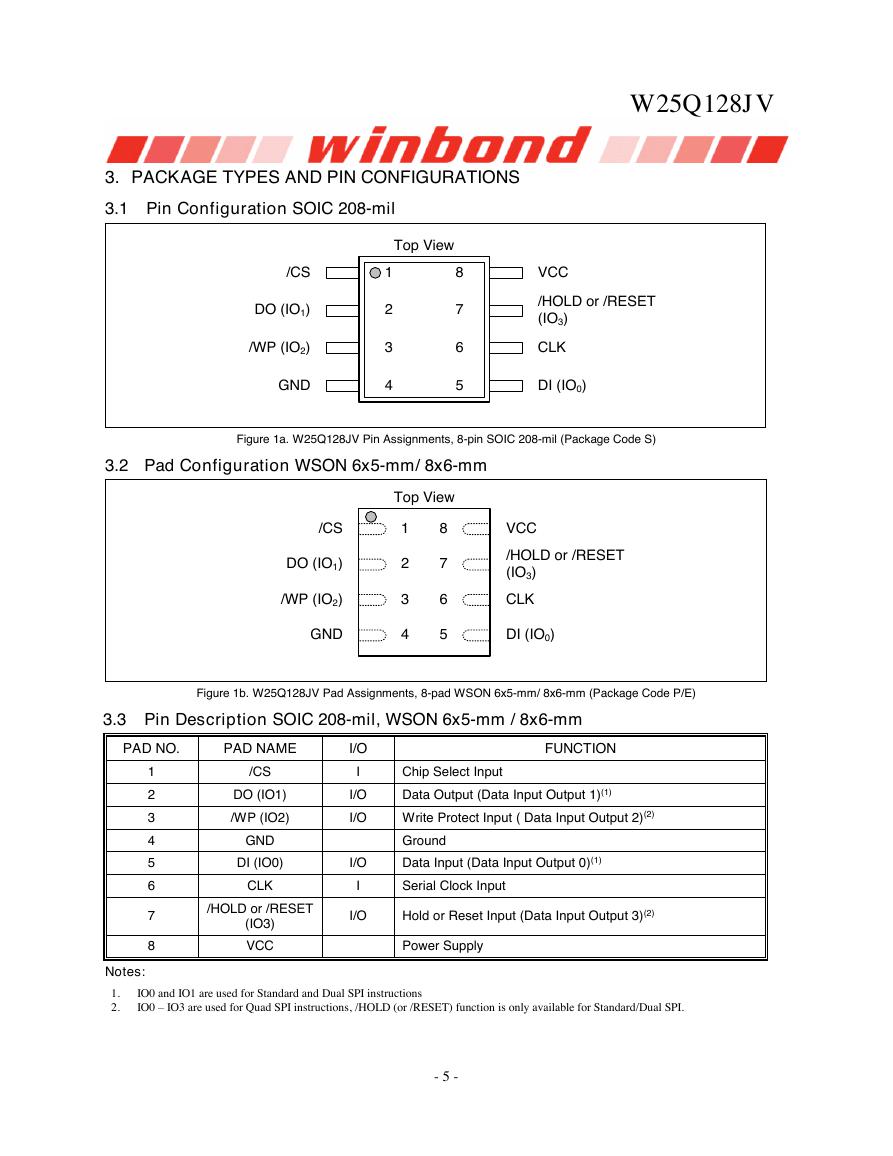
3.1 Pin Configuration SOIC 208-mil
3.2 Pad Configuration WSON 6x5-mm/ 8x6-mm
3.3 Pin Description SOIC 208-mil, WSON 6x5-mm / 8x6-mm
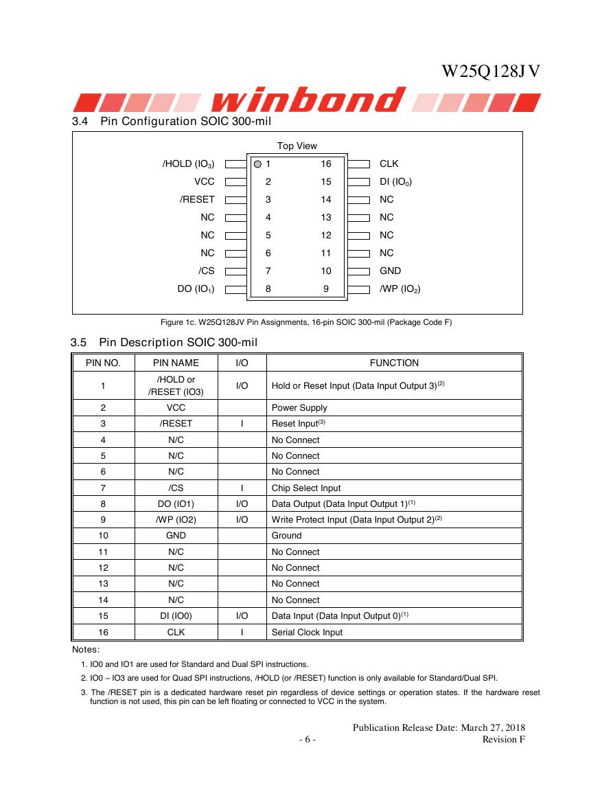
3.4 Pin Configuration SOIC 300-mil
3.5 Pin Description SOIC 300-mil
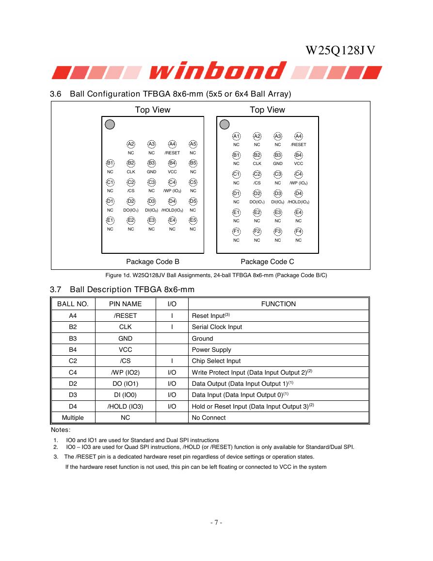
3.6 Ball Configuration TFBGA 8x6-mm (5x5 or 6x4 Ball Array)
3.7 Ball Description TFBGA 8x6-mm
3.8 Ball Configuration WLCSP
3.9 Ball Description WLCSP24
4. pin descriptions
4.1 Chip Select (/CS)
4.2 Serial Data Input, Output and IOs (DI, DO and IO0, IO1, IO2, IO3)
4.3 Write Protect (/WP)
4.4 HOLD (/HOLD)
4.5 Serial Clock (CLK)
4.6 Reset (/RESET)
5. Block Diagram
6. Functional Descriptions
6.1 Standard SPI Instructions
6.2 Dual SPI Instructions
6.3 Quad SPI Instructions
6.4 Software Reset & Hardware /RESET pin
6.5 Write Protection
6.5.1 Write Protect Features
7. Status and configuration Registers
7.1 Status Registers
7.1.1 Erase/Write In Progress (BUSY) – Status Only
7.1.2 Write Enable Latch (WEL) – Status Only
7.1.3 Block Protect Bits (BP2, BP1, BP0) – Volatile/Non-Volatile Writable
7.1.4 Top/Bottom Block Protect (TB) – Volatile/Non-Volatile Writable
7.1.5 Sector/Block Protect Bit (SEC) – Volatile/Non-Volatile Writable
7.1.6 Complement Protect (CMP) – Volatile/Non-Volatile Writable
7.1.1 Status Register Protect (SRP, SRL) – Volatile/Non-Volatile Writable
7.1.2 Erase/Program Suspend Status (SUS) – Status Only
7.1.3 Security Register Lock Bits (LB3, LB2, LB1) – Volatile/Non-Volatile OTP Writable
7.1.4 Quad Enable (QE) – Volatile/Non-Volatile Writable
7.1.5 Write Protect Selection (WPS) – Volatile/Non-Volatile Writable
7.1.6 Output Driver Strength (DRV1, DRV0) – Volatile/Non-Volatile Writable
7.1.7 Reserved Bits – Non Functional
7.1.8 W25Q128JV Status Register Memory Protection (WPS = 0, CMP = 0)
7.1.9 W25Q128JV Status Register Memory Protection (WPS = 0, CMP = 1)
7.1.10 W25Q128JV Individual Block Memory Protection (WPS=1)
8. INSTRUCTIONS
8.1 Device ID and Instruction Set Tables
8.1.1 Manufacturer and Device Identification
8.1.2 Instruction Set Table 1 (Standard SPI Instructions)(1)
8.1.3 Instruction Set Table 2 (Dual/Quad SPI Instructions)
Notes:
8.2 Instruction Descriptions
8.2.1 Write Enable (06h)
8.2.2 Write Enable for Volatile Status Register (50h)
8.2.3 Write Disable (04h)
8.2.4 Read Status Register-1 (05h), Status Register-2 (35h) & Status Register-3 (15h)
8.2.5 Write Status Register-1 (01h), Status Register-2 (31h) & Status Register-3 (11h)
8.2.6 Read Data (03h)
8.2.7 Fast Read (0Bh)
8.2.8 Fast Read Dual Output (3Bh)
8.2.9 Fast Read Quad Output (6Bh)
8.2.10 Fast Read Dual I/O (BBh)
8.2.11 Fast Read Quad I/O (EBh)
8.2.12 Set Burst with Wrap (77h)
8.2.13 Page Program (02h)
8.2.14 Quad Input Page Program (32h)
8.2.15 Sector Erase (20h)
8.2.16 32KB Block Erase (52h)
8.2.17 64KB Block Erase (D8h)
8.2.18 Chip Erase (C7h / 60h)
8.2.19 Erase / Program Suspend (75h)
8.2.20 Erase / Program Resume (7Ah)
8.2.21 Power-down (B9h)
8.2.22 Release Power-down / Device ID (ABh)
8.2.23 Read Manufacturer / Device ID (90h)
8.2.24 Read Manufacturer / Device ID Dual I/O (92h)
8.2.25 Read Manufacturer / Device ID Quad I/O (94h)
8.2.26 Read Unique ID Number (4Bh)
8.2.27 Read JEDEC ID (9Fh)
8.2.28 Read SFDP Register (5Ah)
8.2.29 Erase Security Registers (44h)
8.2.30 Program Security Registers (42h)
8.2.31 Read Security Registers (48h)
8.2.32 Individual Block/Sector Lock (36h)
8.2.33 Individual Block/Sector Unlock (39h)
8.2.34 Read Block/Sector Lock (3Dh)
8.2.35 Global Block/Sector Lock (7Eh)
8.2.36 Global Block/Sector Unlock (98h)
8.2.37 Enable Reset (66h) and Reset Device (99h)
9. Electrical CharacteristicS
9.1 Absolute Maximum Ratings (1)
9.2 Operating Ranges
9.3 Power-Up Power-Down Timing and Requirements
9.4 DC Electrical Characteristics-
9.5 AC Measurement Conditions
9.6 AC Electrical Characteristics(6)
9.7 Serial Output Timing
9.8 Serial Input Timing
9.9 /WP Timing
10. PACKAGE SPECIFICATIONs
10.1 8-Pin SOIC 208-mil (Package Code S)
10.2 16-Pin SOIC 300-mil (Package Code F)
10.3 8-Pad WSON 6x5-mm (Package Code P)
10.4 8-Pad WSON 8x6-mm (Package Code E)
10.5 24-Ball TFBGA 8x6-mm (Package Code B, 5x5-1 ball array)
10.6 24-Ball TFBGA 8x6-mm (Package Code C, 6x4 ball array)
10.7 24-Ball WLCSP (Package Code Y)
11. Ordering Information
11.1 Valid Part Numbers and Top Side Marking
12. Revision history
W25Q128JV 3V 128M-BIT SERIAL FLASH MEMORY WITH DUAL/QUAD SPI For Industrial & Industrial Plus Grade Publication Release Date: March 27, 2018 Revision F
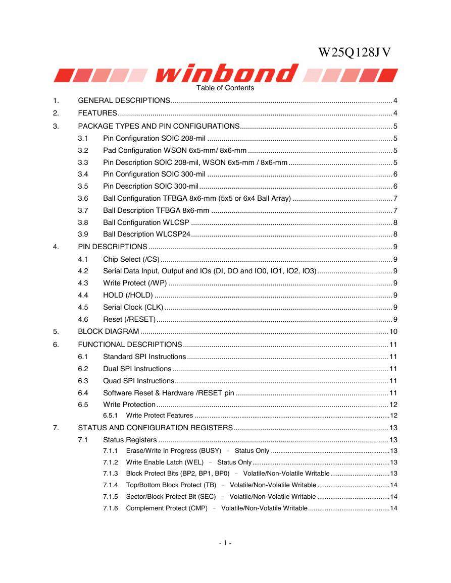
W25Q128JV Table of Contents 1. 2. 3. GENERAL DESCRIPTIONS ............................................................................................................. 4 FEATURES ....................................................................................................................................... 4 PACKAGE TYPES AND PIN CONFIGURATIONS ........................................................................... 5 3.1 3.2 3.3 3.4 3.5 3.6 3.7 3.8 3.9 Pin Configuration SOIC 208-mil ........................................................................................... 5 Pad Configuration WSON 6x5-mm/ 8x6-mm ....................................................................... 5 Pin Description SOIC 208-mil, WSON 6x5-mm / 8x6-mm ................................................... 5 Pin Configuration SOIC 300-mil ........................................................................................... 6 Pin Description SOIC 300-mil ............................................................................................... 6 Ball Configuration TFBGA 8x6-mm (5x5 or 6x4 Ball Array) ................................................. 7 Ball Description TFBGA 8x6-mm ......................................................................................... 7 Ball Configuration WLCSP ................................................................................................... 8 Ball Description WLCSP24 ................................................................................................... 8 4. PIN DESCRIPTIONS ........................................................................................................................ 9 5. 6. 4.1 4.2 Chip Select (/CS) .................................................................................................................. 9 Serial Data Input, Output and IOs (DI, DO and IO0, IO1, IO2, IO3) ..................................... 9 4.3 Write Protect (/WP) .............................................................................................................. 9 4.4 4.5 4.6 HOLD (/HOLD) ..................................................................................................................... 9 Serial Clock (CLK) ................................................................................................................ 9 Reset (/RESET) .................................................................................................................... 9 BLOCK DIAGRAM .......................................................................................................................... 10 FUNCTIONAL DESCRIPTIONS ..................................................................................................... 11 6.1 6.2 6.3 6.4 Standard SPI Instructions ................................................................................................... 11 Dual SPI Instructions .......................................................................................................... 11 Quad SPI Instructions ......................................................................................................... 11 Software Reset & Hardware /RESET pin ........................................................................... 11 6.5 Write Protection .................................................................................................................. 12 6.5.1 Write Protect Features ......................................................................................................... 12 7. STATUS AND CONFIGURATION REGISTERS ............................................................................ 13 7.1 Status Registers ................................................................................................................. 13 7.1.1 Erase/Write In Progress (BUSY) – Status Only ................................................................ 13 7.1.2 Write Enable Latch (WEL) – Status Only .......................................................................... 13 7.1.3 Block Protect Bits (BP2, BP1, BP0) – Volatile/Non-Volatile Writable ................................ 13 7.1.4 Top/Bottom Block Protect (TB) – Volatile/Non-Volatile Writable ....................................... 14 7.1.5 Sector/Block Protect Bit (SEC) – Volatile/Non-Volatile Writable ....................................... 14 7.1.6 Complement Protect (CMP) – Volatile/Non-Volatile Writable ............................................ 14 - 1 -
W25Q128JV 7.1.1 Status Register Protect (SRP, SRL) – Volatile/Non-Volatile Writable ............................... 15 7.1.2 Erase/Program Suspend Status (SUS) – Status Only....................................................... 16 7.1.3 Security Register Lock Bits (LB3, LB2, LB1) – Volatile/Non-Volatile OTP Writable .......... 16 7.1.4 Quad Enable (QE) – Volatile/Non-Volatile Writable .......................................................... 16 7.1.5 Write Protect Selection (WPS) – Volatile/Non-Volatile Writable ....................................... 17 7.1.6 Output Driver Strength (DRV1, DRV0) – Volatile/Non-Volatile Writable ........................... 17 7.1.7 Reserved Bits – Non Functional ........................................................................................ 17 7.1.8 W25Q128JV Status Register Memory Protection (WPS = 0, CMP = 0) ............................... 18 7.1.9 W25Q128JV Status Register Memory Protection (WPS = 0, CMP = 1) ............................... 19 7.1.10 W25Q128JV Individual Block Memory Protection (WPS=1) .............................................. 20 8. INSTRUCTIONS ............................................................................................................................. 21 8.1 8.2 Device ID and Instruction Set Tables ................................................................................. 21 8.1.1 Manufacturer and Device Identification ................................................................................ 21 8.1.2 Instruction Set Table 1 (Standard SPI Instructions)(1)........................................................... 22 8.1.3 Instruction Set Table 2 (Dual/Quad SPI Instructions) ........................................................... 23 Notes: ................................................................................................................................................ 23 Instruction Descriptions ...................................................................................................... 24 8.2.1 Write Enable (06h) ............................................................................................................... 24 8.2.2 Write Enable for Volatile Status Register (50h) .................................................................... 24 8.2.3 Write Disable (04h) ............................................................................................................... 25 8.2.4 Read Status Register-1 (05h), Status Register-2 (35h) & Status Register-3 (15h) .............. 25 8.2.5 Write Status Register-1 (01h), Status Register-2 (31h) & Status Register-3 (11h) .............. 26 8.2.6 Read Data (03h) ................................................................................................................... 28 8.2.7 Fast Read (0Bh) ................................................................................................................... 29 8.2.8 Fast Read Dual Output (3Bh) ............................................................................................... 30 8.2.9 Fast Read Quad Output (6Bh) .............................................................................................. 31 8.2.10 Fast Read Dual I/O (BBh) ................................................................................................... 32 8.2.11 Fast Read Quad I/O (EBh) ................................................................................................. 33 8.2.12 Set Burst with Wrap (77h) .................................................................................................. 35 8.2.13 Page Program (02h) ........................................................................................................... 36 8.2.14 Quad Input Page Program (32h) ........................................................................................ 37 8.2.15 Sector Erase (20h) ............................................................................................................. 38 8.2.16 32KB Block Erase (52h) ..................................................................................................... 39 8.2.17 64KB Block Erase (D8h) ..................................................................................................... 40 8.2.18 Chip Erase (C7h / 60h) ....................................................................................................... 41 8.2.19 Erase / Program Suspend (75h) ......................................................................................... 42 8.2.20 Erase / Program Resume (7Ah) ......................................................................................... 43 8.2.21 Power-down (B9h) .............................................................................................................. 44 8.2.22 Release Power-down / Device ID (ABh) ............................................................................. 45 8.2.23 Read Manufacturer / Device ID (90h) ................................................................................. 46 Publication Release Date: March 27, 2018 - 2 - Revision F
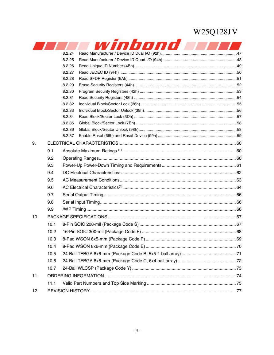
W25Q128JV 8.2.24 Read Manufacturer / Device ID Dual I/O (92h) ................................................................... 47 8.2.25 Read Manufacturer / Device ID Quad I/O (94h) ................................................................. 48 8.2.26 Read Unique ID Number (4Bh)........................................................................................... 49 8.2.27 Read JEDEC ID (9Fh) ........................................................................................................ 50 8.2.28 Read SFDP Register (5Ah) ................................................................................................ 51 8.2.29 Erase Security Registers (44h) ........................................................................................... 52 8.2.30 Program Security Registers (42h) ...................................................................................... 53 8.2.31 Read Security Registers (48h) ........................................................................................... 54 8.2.32 Individual Block/Sector Lock (36h) ..................................................................................... 55 8.2.33 Individual Block/Sector Unlock (39h) .................................................................................. 56 8.2.34 Read Block/Sector Lock (3Dh) ........................................................................................... 57 8.2.35 Global Block/Sector Lock (7Eh) .......................................................................................... 58 8.2.36 Global Block/Sector Unlock (98h) ....................................................................................... 58 8.2.37 Enable Reset (66h) and Reset Device (99h) ...................................................................... 59 9. ELECTRICAL CHARACTERISTICS ............................................................................................... 60 Absolute Maximum Ratings (1) ............................................................................................ 60 Operating Ranges............................................................................................................... 60 9.1 9.2 9.3 9.4 9.5 9.6 9.7 9.8 9.9 Power-Up Power-Down Timing and Requirements ............................................................ 61 DC Electrical Characteristics- ............................................................................................. 62 AC Measurement Conditions .............................................................................................. 63 AC Electrical Characteristics(6) ........................................................................................... 64 Serial Output Timing ........................................................................................................... 66 Serial Input Timing .............................................................................................................. 66 /WP Timing ......................................................................................................................... 66 10. PACKAGE SPECIFICATIONS ........................................................................................................ 67 10.1 8-Pin SOIC 208-mil (Package Code S) .............................................................................. 67 10.2 16-Pin SOIC 300-mil (Package Code F) ............................................................................ 68 10.3 8-Pad WSON 6x5-mm (Package Code P) ......................................................................... 69 10.4 8-Pad WSON 8x6-mm (Package Code E) ......................................................................... 70 10.5 24-Ball TFBGA 8x6-mm (Package Code B, 5x5-1 ball array) ............................................ 71 10.6 24-Ball TFBGA 8x6-mm (Package Code C, 6x4 ball array) ............................................... 72 10.7 24-Ball WLCSP (Package Code Y) .................................................................................... 73 11. ORDERING INFORMATION .......................................................................................................... 74 11.1 Valid Part Numbers and Top Side Marking ........................................................................ 75 12. REVISION HISTORY ...................................................................................................................... 77 - 3 -
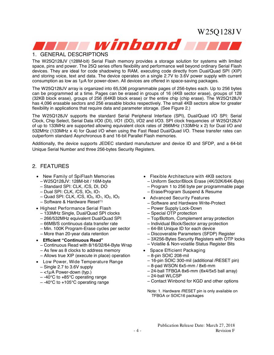
W25Q128JV 1. GENERAL DESCRIPTIONS The W25Q128JV (128M-bit) Serial Flash memory provides a storage solution for systems with limited space, pins and power. The 25Q series offers flexibility and performance well beyond ordinary Serial Flash devices. They are ideal for code shadowing to RAM, executing code directly from Dual/Quad SPI (XIP) and storing voice, text and data. The device operates on a single 2.7V to 3.6V power supply with current consumption as low as 1µA for power-down. All devices are offered in space-saving packages. The W25Q128JV array is organized into 65,536 programmable pages of 256-bytes each. Up to 256 bytes can be programmed at a time. Pages can be erased in groups of 16 (4KB sector erase), groups of 128 (32KB block erase), groups of 256 (64KB block erase) or the entire chip (chip erase). The W25Q128JV has 4,096 erasable sectors and 256 erasable blocks respectively. The small 4KB sectors allow for greater flexibility in applications that require data and parameter storage. (See Figure 2.) The W25Q128JV supports the standard Serial Peripheral Interface (SPI), Dual/Quad I/O SPI: Serial Clock, Chip Select, Serial Data I/O0 (DI), I/O1 (DO), I/O2 and I/O3. SPI clock frequencies of W25Q128JV of up to 133MHz are supported allowing equivalent clock rates of 266MHz (133MHz x 2) for Dual I/O and 532MHz (133MHz x 4) for Quad I/O when using the Fast Read Dual/Quad I/O. These transfer rates can outperform standard Asynchronous 8 and 16-bit Parallel Flash memories. Additionally, the device supports JEDEC standard manufacturer and device ID and SFDP, and a 64-bit Unique Serial Number and three 256-bytes Security Registers. 2. FEATURES – W25Q128JV: 128M-bit / 16M-byte – Standard SPI: CLK, /CS, DI, DO – Dual SPI: CLK, /CS, IO0, IO1 – Quad SPI: CLK, /CS, IO0, IO1, IO2, IO3 – Software & Hardware Reset(1)  Highest Performance Serial Flash – 133MHz Single, Dual/Quad SPI clocks – 266/532MHz equivalent Dual/Quad SPI – 66MB/S continuous data transfer rate – Min. 100K Program-Erase cycles per sector – More than 20-year data retention  Efficient “Continuous Read” – Continuous Read with 8/16/32/64-Byte Wrap – As few as 8 clocks to address memory – Allows true XIP (execute in place) operation  Low Power, Wide Temperature Range – Single 2.7 to 3.6V supply – <1µA Power-down (typ.) – -40°C to +85°C operating range – -40°C to +105°C operating range  New Family of SpiFlash Memories  Flexible Architecture with 4KB sectors – Uniform Sector/Block Erase (4K/32K/64K-Byte) – Program 1 to 256 byte per programmable page – Erase/Program Suspend & Resume  Advanced Security Features – Software and Hardware Write-Protect – Power Supply Lock-Down – Special OTP protection – Top/Bottom, Complement array protection – Individual Block/Sector array protection – 64-Bit Unique ID for each device – Discoverable Parameters (SFDP) Register – 3X256-Bytes Security Registers with OTP locks – Volatile & Non-volatile Status Register Bits  Space Efficient Packaging – 8-pin SOIC 208-mil – 16-pin SOIC 300-mil (additional /RESET pin) – 8-pad WSON 6x5-mm / 8x6-mm – 24-ball TFBGA 8x6-mm (6x4/5x5 ball array) – 24-ball WLCSP – Contact Winbond for KGD and other options Note: 1. Hardware /RESET pin is only available on TFBGA or SOIC16 packages Publication Release Date: March 27, 2018 - 4 - Revision F
3. PACKAGE TYPES AND PIN CONFIGURATIONS 3.1 Pin Configuration SOIC 208-mil W25Q128JV Figure 1a. W25Q128JV Pin Assignments, 8-pin SOIC 208-mil (Package Code S) 3.2 Pad Configuration WSON 6x5-mm/ 8x6-mm Figure 1b. W25Q128JV Pad Assignments, 8-pad WSON 6x5-mm/ 8x6-mm (Package Code P/E) 3.3 Pin Description SOIC 208-mil, WSON 6x5-mm / 8x6-mm PAD NO. PAD NAME 1 2 3 4 5 6 7 8 Notes: /CS DO (IO1) /WP (IO2) GND DI (IO0) CLK /HOLD or /RESET (IO3) VCC I/O I I/O I/O I/O I I/O FUNCTION Chip Select Input Data Output (Data Input Output 1)(1) Write Protect Input ( Data Input Output 2)(2) Ground Data Input (Data Input Output 0)(1) Serial Clock Input Hold or Reset Input (Data Input Output 3)(2) Power Supply 1. 2. IO0 and IO1 are used for Standard and Dual SPI instructions IO0 – IO3 are used for Quad SPI instructions, /HOLD (or /RESET) function is only available for Standard/Dual SPI. - 5 - 12348765/CSDO (IO1)/WP (IO2)GNDVCC/HOLD or /RESET(IO3)DI (IO0)CLKTop View 1234/CSDO (IO1)/WP (IO2)GNDVCC/HOLD or /RESET(IO3)DI (IO0)CLKTop View 8765
3.4 Pin Configuration SOIC 300-mil W25Q128JV Figure 1c. W25Q128JV Pin Assignments, 16-pin SOIC 300-mil (Package Code F) 3.5 Pin Description SOIC 300-mil PIN NO. PIN NAME 1 2 3 4 5 6 7 8 9 10 11 12 13 14 15 16 /HOLD or /RESET (IO3) VCC /RESET N/C N/C N/C /CS DO (IO1) /WP (IO2) GND N/C N/C N/C N/C DI (IO0) CLK I/O I/O I I I/O I/O I/O I FUNCTION Hold or Reset Input (Data Input Output 3)(2) Power Supply Reset Input(3) No Connect No Connect No Connect Chip Select Input Data Output (Data Input Output 1)(1) Write Protect Input (Data Input Output 2)(2) Ground No Connect No Connect No Connect No Connect Data Input (Data Input Output 0)(1) Serial Clock Input Notes: 1. IO0 and IO1 are used for Standard and Dual SPI instructions. 2. IO0 – IO3 are used for Quad SPI instructions, /HOLD (or /RESET) function is only available for Standard/Dual SPI. 3. The /RESET pin is a dedicated hardware reset pin regardless of device settings or operation states. If the hardware reset function is not used, this pin can be left floating or connected to VCC in the system. Publication Release Date: March 27, 2018 - 6 - Revision F 1234/CSDO (IO1)/WP (IO2)GNDVCC/HOLD (IO3)DI (IO0)CLKTop View NC/RESETNCNCNCNCNCNC5678109111213141516
3.6 Ball Configuration TFBGA 8x6-mm (5x5 or 6x4 Ball Array) W25Q128JV Figure 1d. W25Q128JV Ball Assignments, 24-ball TFBGA 8x6-mm (Package Code B/C) 3.7 Ball Description TFBGA 8x6-mm BALL NO. PIN NAME I/O FUNCTION A4 B2 B3 B4 C2 C4 D2 D3 D4 /RESET CLK GND VCC /CS /WP (IO2) DO (IO1) DI (IO0) /HOLD (IO3) Multiple NC Notes: I I I I/O I/O I/O I/O Reset Input(3) Serial Clock Input Ground Power Supply Chip Select Input Write Protect Input (Data Input Output 2)(2) Data Output (Data Input Output 1)(1) Data Input (Data Input Output 0)(1) Hold or Reset Input (Data Input Output 3)(2) No Connect 1. 2. IO0 and IO1 are used for Standard and Dual SPI instructions IO0 – IO3 are used for Quad SPI instructions, /HOLD (or /RESET) function is only available for Standard/Dual SPI. 3. The /RESET pin is a dedicated hardware reset pin regardless of device settings or operation states. If the hardware reset function is not used, this pin can be left floating or connected to VCC in the system - 7 - D1/HOLD(IO3)DI(IO0)DO(IO1)/WP (IO2)D2D3D4NCE1NCNCNCE2E3E4NCF1NCNCNCF2F3F4NCA1/RESETNCNCA2A3A4NCB1VCCGNDCLKB2B3B4NCC1NC/CSC2C3C4NCTop ViewPackage Code CTop ViewD1/HOLD(IO3)DI(IO0)DO(IO1)/WP (IO2)D2D3D4NCE1NCNCNCE2E3E4NC/RESETNCNCA2A3A4B1VCCGNDCLKB2B3B4NCC1NC/CSC2C3C4NCD5E5A5B5C5NCNCNCNCNCPackage Code B
分享到:
收藏