www.ti.com
SBAS367F –JUNE 2007–REVISED FEBRUARY 2011
Quad/Octal, Simultaneous Sampling, 24-Bit Analog-to-Digital Converters
Check for Samples: ADS1274, ADS1278
ADS1274
ADS1278
1FEATURES
234• Simultaneously Measure Four/Eight Channels
• Up to 144kSPS Data Rate
• AC Performance:
70kHz Bandwidth
111dB SNR (High-Resolution Mode)
–108dB THD
• DC Accuracy:
0.8μV/°C Offset Drift
1.3ppm/°C Gain Drift
• Selectable Operating Modes:
High-Speed: 144kSPS, 106dB SNR
High-Resolution: 52kSPS, 111dB SNR
Low-Power: 52kSPS, 31mW/ch
Low-Speed: 10kSPS, 7mW/ch
• Linear Phase Digital Filter
• SPI™ or Frame-Sync Serial Interface
• Low Sampling Aperture Error
• Modulator Output Option (digital filter bypass)
• Analog Supply: 5V
• Digital Core: 1.8V
•
I/O Supply: 1.8V to 3.3V
APPLICATIONS
• Vibration/Modal Analysis
• Multi-Channel Data Acquisition
• Acoustics/Dynamic Strain Gauges
• Pressure Sensors
and
for
in
are mostly
DESCRIPTION
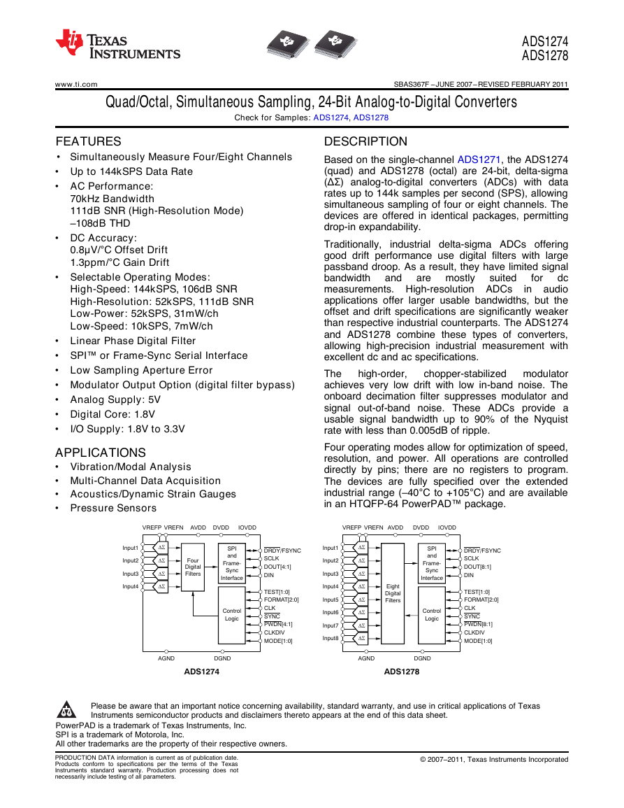
Based on the single-channel ADS1271, the ADS1274
(quad) and ADS1278 (octal) are 24-bit, delta-sigma
(ΔΣ) analog-to-digital converters (ADCs) with data
rates up to 144k samples per second (SPS), allowing
simultaneous sampling of four or eight channels. The
devices are offered in identical packages, permitting
drop-in expandability.
Traditionally,
industrial delta-sigma ADCs offering
good drift performance use digital filters with large
passband droop. As a result, they have limited signal
bandwidth
suited
dc
measurements. High-resolution ADCs
audio
applications offer larger usable bandwidths, but the
offset and drift specifications are significantly weaker
than respective industrial counterparts. The ADS1274
and ADS1278 combine these types of converters,
allowing high-precision industrial measurement with
excellent dc and ac specifications.
The
chopper-stabilized modulator
achieves very low drift with low in-band noise. The
onboard decimation filter suppresses modulator and
signal out-of-band noise. These ADCs provide a
usable signal bandwidth up to 90% of the Nyquist
rate with less than 0.005dB of ripple.
Four operating modes allow for optimization of speed,
resolution, and power. All operations are controlled
directly by pins; there are no registers to program.
The devices are fully specified over the extended
industrial range (–40°C to +105°C) and are available
in an HTQFP-64 PowerPAD™ package.
high-order,
1
Please be aware that an important notice concerning availability, standard warranty, and use in critical applications of Texas
Instruments semiconductor products and disclaimers thereto appears at the end of this data sheet.
2PowerPAD is a trademark of Texas Instruments, Inc.
3SPI is a trademark of Motorola, Inc.
4All other trademarks are the property of their respective owners.
PRODUCTION DATA information is current as of publication date.
Products conform to specifications per the terms of
the Texas
Instruments standard warranty. Production processing does not
necessarily include testing of all parameters.
© 2007–2011, Texas Instruments Incorporated
VREFPVREFNAVDDDVDDTEST[1:0]FORMAT[2:0]CLKSYNCPWDN[8:1]CLKDIVControlLogicSPIandFrame-SyncInterfaceIOVDDDGNDAGNDDRDY/FSYNCSCLKDOUT[8:1]DINInput2Input1Input4Input3Input6Input5Input8Input7DSDSDSDSDSDSDSDSPWDN[4:1]ADS1278FourDigitalFiltersAVDDDVDDTEST[1:0]FORMAT[2:0]CLKSYNCCLKDIVControlLogicSPIandFrame-SyncInterfaceIOVDDDGNDAGNDDRDY/FSYNCSCLKDOUT[4:1]DINADS1274MODE[1:0]MODE[1:0]EightDigitalFiltersVREFPVREFNInput2Input1Input4Input3DSDSDSDS�
ADS1274
ADS1278
SBAS367F –JUNE 2007–REVISED FEBRUARY 2011
www.ti.com
This integrated circuit can be damaged by ESD. Texas Instruments recommends that all
appropriate precautions. Failure to observe proper handling and installation procedures can cause damage.
integrated circuits be handled with
ESD damage can range from subtle performance degradation to complete device failure. Precision integrated circuits may be more
susceptible to damage because very small parametric changes could cause the device not to meet its published specifications.
For the most current package and ordering information, see the Package Option Addendum at the end of this
document, or visit the device product folder at www.ti.com.
ORDERING INFORMATION
ABSOLUTE MAXIMUM RATINGS
Over operating free-air temperature range unless otherwise noted (1)
AVDD to AGND
DVDD, IOVDD to DGND
AGND to DGND
Input current
Analog input to AGND
Digital input or output to DGND
Maximum junction temperature
Operating temperature range
Storage temperature range
Momentary
Continuous
ADS1274
ADS1278
ADS1274, ADS1278
UNIT
–0.3 to +6.0
–0.3 to +3.6
–0.3 to +0.3
100
10
–0.3 to AVDD + 0.3
–0.3 to IOVDD + 0.3
+150
–40 to +125
–40 to +105
–60 to +150
V
V
V
mA
mA
V
V
°C
°C
°C
°C
(1) Stresses above these ratings may cause permanent damage. Exposure to absolute maximum conditions for extended periods may
degrade device reliability. These are stress ratings only, and functional operation of the device at these or any other conditions beyond
those specified is not implied.
2
Submit Documentation Feedback
© 2007–2011, Texas Instruments Incorporated
Product Folder Link(s): ADS1274 ADS1278
�
ADS1274
ADS1278
www.ti.com
SBAS367F –JUNE 2007–REVISED FEBRUARY 2011
ELECTRICAL CHARACTERISTICS
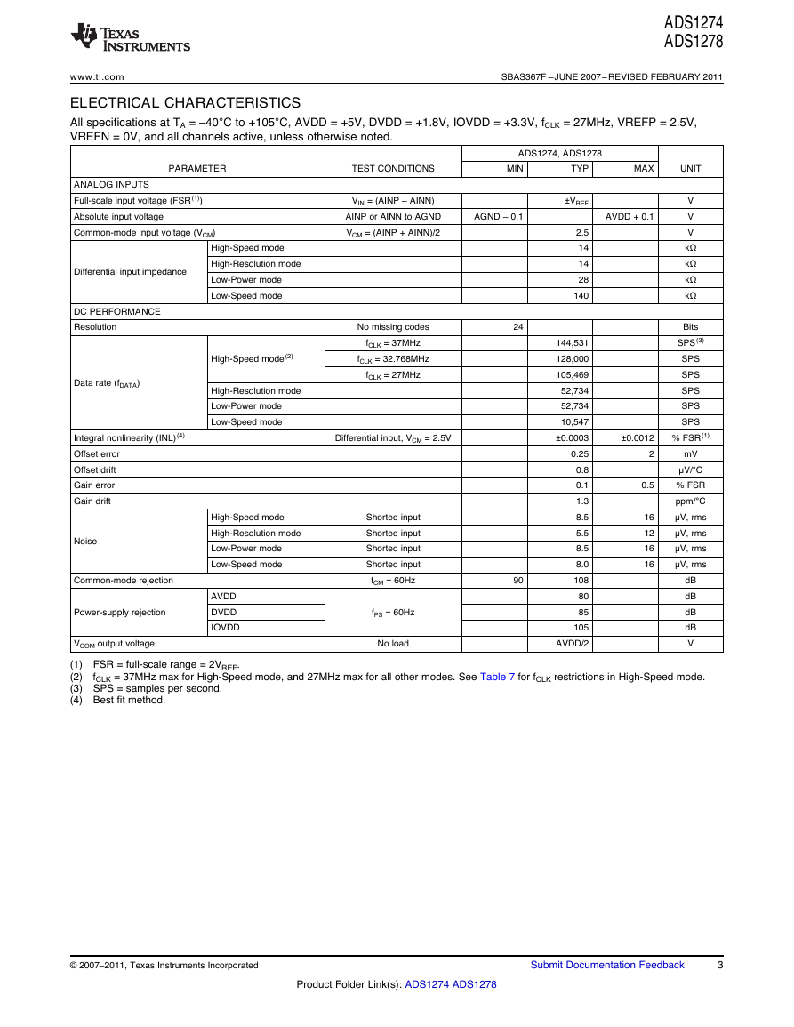
All specifications at TA = –40°C to +105°C, AVDD = +5V, DVDD = +1.8V, IOVDD = +3.3V, fCLK = 27MHz, VREFP = 2.5V,
VREFN = 0V, and all channels active, unless otherwise noted.
PARAMETER
TEST CONDITIONS
MIN
TYP
MAX
UNIT
ADS1274, ADS1278
ANALOG INPUTS
Full-scale input voltage (FSR (1))
Absolute input voltage
Common-mode input voltage (VCM)
VIN = (AINP – AINN)
AINP or AINN to AGND
VCM = (AINP + AINN)/2
Differential input impedance
DC PERFORMANCE
Resolution
Data rate (fDATA)
Integral nonlinearity (INL) (4)
Offset error
Offset drift
Gain error
Gain drift
Noise
High-Speed mode
High-Resolution mode
Low-Power mode
Low-Speed mode
High-Speed mode (2)
High-Resolution mode
Low-Power mode
Low-Speed mode
High-Speed mode
High-Resolution mode
Low-Power mode
Low-Speed mode
Common-mode rejection
Power-supply rejection
VCOM output voltage
AVDD
DVDD
IOVDD
No missing codes
fCLK = 37MHz
fCLK = 32.768MHz
fCLK = 27MHz
Differential input, VCM = 2.5V
Shorted input
Shorted input
Shorted input
Shorted input
fCM = 60Hz
fPS = 60Hz
No load
±VREF
AGND – 0.1
AVDD + 0.1
2.5
14
14
28
140
144,531
128,000
105,469
52,734
52,734
10,547
±0.0003
0.25
0.8
0.1
1.3
8.5
5.5
8.5
8.0
108
80
85
105
AVDD/2
24
90
±0.0012
2
0.5
16
12
16
16
V
V
V
kΩ
kΩ
kΩ
kΩ
Bits
SPS (3)
SPS
SPS
SPS
SPS
SPS
% FSR (1)
mV
μV/°C
% FSR
ppm/°C
μV, rms
μV, rms
μV, rms
μV, rms
dB
dB
dB
dB
V
fCLK = 37MHz max for High-Speed mode, and 27MHz max for all other modes. See Table 7 for fCLK restrictions in High-Speed mode.
(1) FSR = full-scale range = 2VREF.
(2)
(3) SPS = samples per second.
(4) Best fit method.
© 2007–2011, Texas Instruments Incorporated
Submit Documentation Feedback
3
Product Folder Link(s): ADS1274 ADS1278
�
ADS1274
ADS1278
SBAS367F –JUNE 2007–REVISED FEBRUARY 2011
www.ti.com
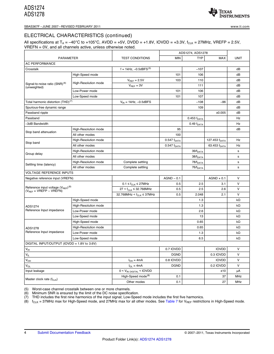
ELECTRICAL CHARACTERISTICS (continued)
All specifications at TA = –40°C to +105°C, AVDD = +5V, DVDD = +1.8V, IOVDD = +3.3V, fCLK = 27MHz, VREFP = 2.5V,
VREFN = 0V, and all channels active, unless otherwise noted.
ADS1274, ADS1278
MAX
UNIT
PARAMETER
TEST CONDITIONS
AC PERFORMANCE
Crosstalk
Signal-to-noise ratio (SNR) (6)
(unweighted)
Total harmonic distortion (THD) (7)
Spurious-free dynamic range
High-Speed mode
High-Resolution mode
Low-Power mode
Low-Speed mode
f = 1kHz, –0.5dBFS (5)
VREF = 2.5V
VREF = 3V
VIN = 1kHz, –0.5dBFS
Passband ripple
Passband
–3dB Bandwidth
Stop band attenuation
Stop band
Group delay
Settling time (latency)
High-Resolution mode
All other modes
High-Resolution mode
All other modes
High-Resolution mode
All other modes
High-Resolution mode
All other modes
VOLTAGE REFERENCE INPUTS
Negative reference input (VREFN)
Reference input voltage (VREF) (8)
(VREF = VREFP – VREFN)
ADS1274
Reference Input impedance
ADS1278
Reference Input impedance
High-Speed mode
High-Resolution mode
Low-Power mode
Low-Speed mode
High-Speed mode
High-Resolution mode
Low-Power mode
Low-Speed mode
DIGITAL INPUT/OUTPUT (IOVDD = 1.8V to 3.6V)
VIH
VIL
VOH
VOL
Input leakage
Master clock rate (fCLK)
MIN
101
103
101
101
TYP
–107
106
110
111
106
107
–108
109
0.453 fDATA
0.49 fDATA
95
100
0.547 fDATA
0.547 fDATA
–96
±0.005
127.453 fDATA
63.453 fDATA
AGND + 0.1
3.1
2.6
2.1
Complete settling
Complete settling
0.1 ≤ fCLK ≤ 27MHz
27 < fCLK ≤ 32.768MHz
32.768MHz < fCLK ≤ 37MHz
AGND – 0.1
0.5
0.5
0.5
39/fDATA
38/fDATA
78/fDATA
76/fDATA
2.5
2.5
2.048
1.3
1.3
2.6
13
0.65
0.65
1.3
6.5
IOH = 4mA
IOL = 4mA
0 < VIN DIGITAL < IOVDD
High-Speed mode(8)
Other modes
0.7 IOVDD
DGND
0.8 IOVDD
DGND
0.1
0.1
IOVDD
0.3 IOVDD
IOVDD
0.2 IOVDD
±10
37
27
dB
dB
dB
dB
dB
dB
dB
dB
dB
Hz
Hz
dB
Hz
Hz
s
s
s
s
V
V
V
V
kΩ
kΩ
kΩ
kΩ
kΩ
kΩ
kΩ
kΩ
V
V
V
V
μA
MHz
MHz
(5) Worst-case channel crosstalk between one or more channels.
(6) Minimum SNR is ensured by the limit of the DC noise specification.
(7) THD includes the first nine harmonics of the input signal; Low-Speed mode includes the first five harmonics.
(8)
fCLK = 37MHz max for High-Speed mode, and 27MHz max for all other modes. See Table 7 for VREF restrictions in High-Speed mode.
4
Submit Documentation Feedback
© 2007–2011, Texas Instruments Incorporated
Product Folder Link(s): ADS1274 ADS1278
�
www.ti.com
SBAS367F –JUNE 2007–REVISED FEBRUARY 2011
ELECTRICAL CHARACTERISTICS (continued)
All specifications at TA = –40°C to +105°C, AVDD = +5V, DVDD = +1.8V, IOVDD = +3.3V, fCLK = 27MHz, VREFP = 2.5V,
VREFN = 0V, and all channels active, unless otherwise noted.
ADS1274, ADS1278
ADS1274
ADS1278
POWER SUPPLY
AVDD
DVDD (9)
IOVDD
Power-down current
ADS1274
ADS1274
AVDD current
ADS1274
DVDD current
ADS1274
IOVDD current
ADS1274
Power dissipation
ADS1278
ADS1278
AVDD current
ADS1278
DVDD current
ADS1278
IOVDD current
ADS1278
Power dissipation
PARAMETER
TEST CONDITIONS
0.1 ≤ fCLK ≤ 32.768MHz
32.768MHz < fCLK ≤ 37MHz
MIN
4.75
1.65
2.0
1.65
AVDD
DVDD
IOVDD
High-Speed mode
High-Resolution mode
Low-Power mode
Low-Speed mode
High-Speed mode
High-Resolution mode
Low-Power mode
Low-Speed mode
High-Speed mode
High-Resolution mode
Low-Power mode
Low-Speed mode
High-Speed mode
High-Resolution mode
Low-Power mode
Low-Speed mode
High-Speed mode
High-Resolution mode
Low-Power mode
Low-Speed mode
High-Speed mode
High-Resolution mode
Low-Power mode
Low-Speed mode
High-Speed mode
High-Resolution mode
Low-Power mode
Low-Speed mode
High-Speed mode
High-Resolution mode
Low-Power mode
Low-Speed mode
TYP
MAX
UNIT
5
1.8
2.1
1
1
1
50
50
23
5
18
12
10
2.5
0.15
0.075
0.075
0.02
285
275
135
30
97
97
44
9
23
16
12
2.5
0.25
0.125
0.125
0.035
530
515
245
50
5.25
1.95
2.2
3.6
10
15
10
75
75
35
9
24
17
15
4.5
0.5
0.3
0.3
0.15
420
410
210
55
145
145
64
14
30
20
17
4.5
1
0.5
0.5
0.2
785
765
355
80
V
V
V
V
μA
μA
μA
mA
mA
mA
mA
mA
mA
mA
mA
mA
mA
mA
mA
mW
mW
mW
mW
mA
mA
mA
mA
mA
mA
mA
mA
mA
mA
mA
mA
mW
mW
mW
mW
(9)
fCLK = 37MHz max for High-Speed mode, and 27MHz max for all other modes. See Table 7 for DVDD restrictions in High-Speed mode.
© 2007–2011, Texas Instruments Incorporated
Submit Documentation Feedback
5
Product Folder Link(s): ADS1274 ADS1278
�
ADS1274
ADS1278
SBAS367F –JUNE 2007–REVISED FEBRUARY 2011
www.ti.com
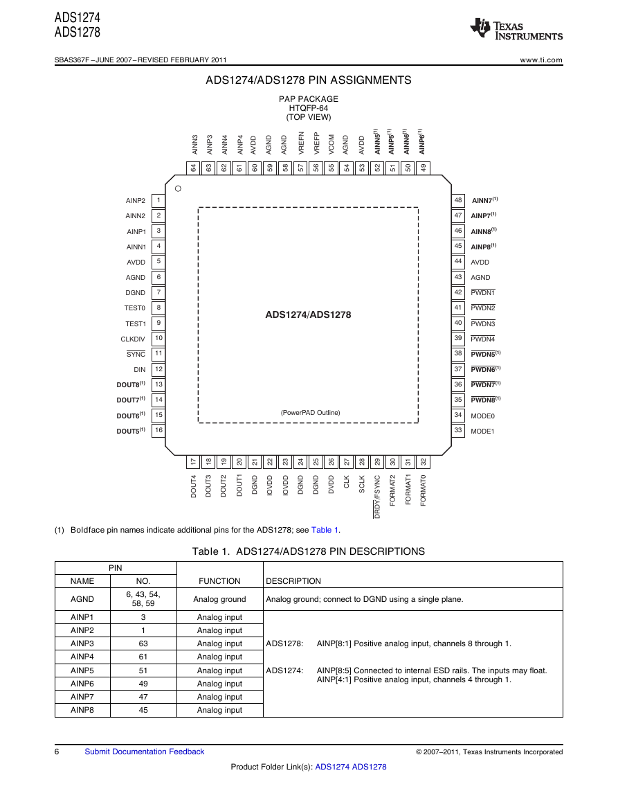
ADS1274/ADS1278 PIN ASSIGNMENTS
PAP PACKAGE
HTQFP-64
(TOP VIEW)
(1) Boldface pin names indicate additional pins for the ADS1278; see Table 1.
PIN
NO.
6, 43, 54,
58, 59
3
1
63
61
51
49
47
45
NAME
AGND
AINP1
AINP2
AINP3
AINP4
AINP5
AINP6
AINP7
AINP8
Table 1. ADS1274/ADS1278 PIN DESCRIPTIONS
FUNCTION
DESCRIPTION
Analog ground
Analog ground; connect to DGND using a single plane.
Analog input
Analog input
Analog input
Analog input
Analog input
Analog input
Analog input
Analog input
ADS1278:
AINP[8:1] Positive analog input, channels 8 through 1.
ADS1274:
AINP[8:5] Connected to internal ESD rails. The inputs may float.
AINP[4:1] Positive analog input, channels 4 through 1.
6
Submit Documentation Feedback
© 2007–2011, Texas Instruments Incorporated
Product Folder Link(s): ADS1274 ADS1278
AINN7(1)AINP7(1)AINN8(1)AINP8(1)AVDDAGNDPWDN1PWDN2PWDN3PWDN4PWDN5(1)PWDN6(1)PWDN7(1)PWDN8(1)MODE0MODE1AINP2AINN2AINP1AINN1AVDDAGNDDGNDTEST0TEST1CLKDIVSYNCDINDOUT8(1)DOUT7(1)DOUT6(1)DOUT5(1)AINN3AINP3AINN4AINP4AVDDAGNDVREFNVREFPVCOMAGNDAVDDAINP5(1)AINN6(1)AINP6(1)AINN5(1)DOUT4DOUT3DOUT2DOUT1DGNDIOVDDIOVDDDGNDDGNDDVDDCLKSCLKDRDY/FSYNCFORMAT2FORMAT1FORMAT0ADS1274/ADS1278AGND12345678910111213141516484746454443424140393837363534331718192021222324252627282930313264636261605958575655545352515049(PowerPAD Outline)�
ADS1274
ADS1278
SBAS367F –JUNE 2007–REVISED FEBRUARY 2011
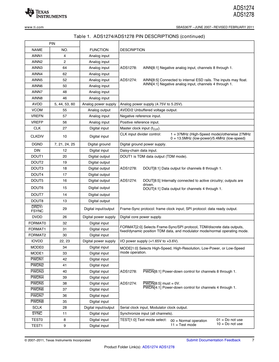
Table 1. ADS1274/ADS1278 PIN DESCRIPTIONS (continued)
www.ti.com
PIN
NAME
AINN1
AINN2
AINN3
AINN4
AINN5
AINN6
AINN7
AINN8
AVDD
VCOM
VREFN
VREFP
CLK
CLKDIV
DGND
DIN
DOUT1
DOUT2
DOUT3
DOUT4
DOUT5
DOUT6
DOUT7
DOUT8
DRDY/
FSYNC
DVDD
FORMAT0
FORMAT1
FORMAT2
IOVDD
MODE0
MODE1
PWDN1
PWDN2
PWDN3
PWDN4
PWDN5
PWDN6
PWDN7
PWDN8
SCLK
SYNC
TEST0
TEST1
NO.
4
2
64
62
52
50
48
46
FUNCTION
Analog input
Analog input
Analog input
Analog input
Analog input
Analog input
Analog input
Analog input
DESCRIPTION
ADS1278:
AINN[8:1] Negative analog input, channels 8 through 1.
ADS1274:
AINN[8:5] Connected to internal ESD rails. The inputs may float.
AINN[4:1] Negative analog input, channels 4 through 1.
5, 44, 53, 60
Analog power supply Analog power supply (4.75V to 5.25V).
55
57
56
27
10
7, 21, 24, 25
12
20
19
18
17
16
15
14
13
29
26
32
31
30
AVDD/2 Unbuffered voltage output.
Negative reference input.
Positive reference input.
Master clock input (fCLK).
CLK input divider control:
1 = 37MHz (High-Speed mode)/otherwise 27MHz
0 = 13.5MHz (low-power)/5.4MHz (low-speed)
Digital ground power supply.
Daisy-chain data input.
DOUT1 is TDM data output (TDM mode).
ADS1278:
DOUT[8:1] Data output for channels 8 through 1.
ADS1274:
DOUT[8:5] Internally connected to active circuitry; outputs are
driven.
DOUT[4:1] Data output for channels 4 through 1.
Analog output
Analog input
Analog input
Digital input
Digital input
Digital ground
Digital input
Digital output
Digital output
Digital output
Digital output
Digital output
Digital output
Digital output
Digital output
Digital input/output
Frame-Sync protocol: frame clock input; SPI protocol: data ready output.
Digital power supply Digital core power supply.
Digital input
Digital input
Digital input
FORMAT[2:0] Selects Frame-Sync/SPI protocol, TDM/discrete data outputs,
fixed/dynamic position TDM data, and modulator mode/normal operating mode.
22, 23
Digital power supply
I/O power supply (+1.65V to +3.6V).
34
33
42
41
40
39
38
37
36
35
28
11
8
9
MODE[1:0] Selects High-Speed, High-Resolution, Low-Power, or Low-Speed
mode operation.
ADS1278:
PWDN[8:1] Power-down control for channels 8 through 1.
ADS1274:
PWDN[8:5] must = 0V.
PWDN[4:1] Power-down control for channels 4 through 1.
Digital input
Digital input
Digital input
Digital input
Digital input
Digital input
Digital input
Digital input
Digital input
Digital input
Digital input/output
Digital input
Digital input
Digital input
Serial clock input, Modulator clock output.
Synchronize input (all channels).
TEST[1:0] Test mode select:
00 = Normal operation
11 = Test mode
01 = Do not use
10 = Do not use
© 2007–2011, Texas Instruments Incorporated
Submit Documentation Feedback
7
Product Folder Link(s): ADS1274 ADS1278
�
ADS1274
ADS1278
SBAS367F –JUNE 2007–REVISED FEBRUARY 2011
www.ti.com
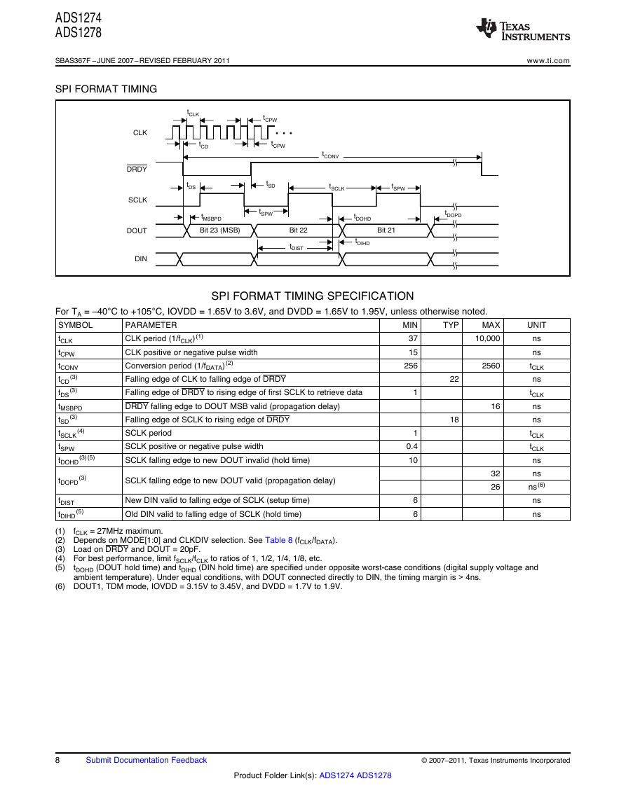
SPI FORMAT TIMING
SPI FORMAT TIMING SPECIFICATION
For TA = –40°C to +105°C, IOVDD = 1.65V to 3.6V, and DVDD = 1.65V to 1.95V, unless otherwise noted.
SYMBOL
tCLK
tCPW
tCONV
(3)
tCD
tDS
tMSBPD
(3)
tSD
tSCLK
tSPW
tDOHD
PARAMETER
CLK period (1/fCLK) (1)
CLK positive or negative pulse width
Conversion period (1/fDATA) (2)
Falling edge of CLK to falling edge of DRDY
Falling edge of DRDY to rising edge of first SCLK to retrieve data
DRDY falling edge to DOUT MSB valid (propagation delay)
Falling edge of SCLK to rising edge of DRDY
SCLK period
SCLK positive or negative pulse width
SCLK falling edge to new DOUT invalid (hold time)
MIN
37
15
256
1
0.4
10
22
18
(4)
(3) (5)
(3)
TYP
MAX
10,000
2560
1
UNIT
ns
ns
tCLK
ns
tCLK
ns
ns
tCLK
tCLK
ns
ns
ns (6)
ns
ns
16
32
26
tDOPD
(3)
tDIST
tDIHD
(5)
SCLK falling edge to new DOUT valid (propagation delay)
New DIN valid to falling edge of SCLK (setup time)
Old DIN valid to falling edge of SCLK (hold time)
6
6
fCLK = 27MHz maximum.
(1)
(2) Depends on MODE[1:0] and CLKDIV selection. See Table 8 (fCLK/fDATA).
(3) Load on DRDY and DOUT = 20pF.
(4) For best performance, limit fSCLK/fCLK to ratios of 1, 1/2, 1/4, 1/8, etc.
(5)
tDOHD (DOUT hold time) and tDIHD (DIN hold time) are specified under opposite worst-case conditions (digital supply voltage and
ambient temperature). Under equal conditions, with DOUT connected directly to DIN, the timing margin is > 4ns.
(6) DOUT1, TDM mode, IOVDD = 3.15V to 3.45V, and DVDD = 1.7V to 1.9V.
8
Submit Documentation Feedback
© 2007–2011, Texas Instruments Incorporated
Product Folder Link(s): ADS1274 ADS1278
CLKtCPWtCLKtCPWtSDtSCLKtDISTtDOHDtSPWBit 23 (MSB)Bit 22Bit 21tSPWtDOPDtCDtDStMSBPDtDIHD· · ·tCONVDRDYSCLKDOUTDIN�



 2023年江西萍乡中考道德与法治真题及答案.doc
 2012年重庆南川中考生物真题及答案.doc
 2013年江西师范大学地理学综合及文艺理论基础考研真题.doc
 2020年四川甘孜小升初语文真题及答案I卷.doc
 2020年注册岩土工程师专业基础考试真题及答案.doc
 2023-2024学年福建省厦门市九年级上学期数学月考试题及答案.doc
 2021-2022学年辽宁省沈阳市大东区九年级上学期语文期末试题及答案.doc
 2022-2023学年北京东城区初三第一学期物理期末试卷及答案.doc
 2018上半年江西教师资格初中地理学科知识与教学能力真题及答案.doc
 2012年河北国家公务员申论考试真题及答案-省级.doc
 2020-2021学年江苏省扬州市江都区邵樊片九年级上学期数学第一次质量检测试题及答案.doc
 2022下半年黑龙江教师资格证中学综合素质真题及答案.doc