DDR3 Pinout Generation Utility
User’s Guide
June 2012
UG62_01.0
�
DDR3 Pinout Generation Utility
Introduction
The DDR3 Pinout Generation Utility is a GUI tool that is capable of generating the pinout and preference files that
contain information for a design that uses the DDR3 SDRAM Controller IP core. The process of determining and
assigning a pinout configuration is not always straightforward. Many factors need to be taken into consideration
such as pinout generation rules, SSN reduction, etc. The DDR3 Pinout Generation Utility aids the user by providing
an automated GUI-based environment that simplifies the pinout generation process. This tool enables the user to
input the desired configuration into the GUI and generates a pinout file and corresponding preference file as the
output. The pinout is generated in the form of an Excel spreadsheet file (.xls). A .lpf file provides the LOCATE pref-
erences for the generated pins.
System Requirements
The following is a list of the system requirements:
• Microsoft Excel 2007 or later (Excel 2010 recommended)
Windows 7 or Windows XP (Windows 7 recommended)
Lattice Diamond® design software, version 1.4 or later
DDR3 SDRAM Controller IP core, version 1.4 or later
Environment Setup
The DDR3 Pinout Generation Utility also provides an automated pinout validation feature. Once a DDR3 pinout is
generated, you can use the Diamond software and the DDR3 SDRAM Controller IP core to validate the generated
pinout. Before the tool can be put into use, certain settings and variables need to be configured. The procedure to
set up the required options for accessing the Diamond software and the DDR3 SDRAM Controller IP core is pro-
vided below. Note that this flow is for the Windows 7 platform. If you use a different operating system, you can take
equivalent steps.
Setup for Diamond Access
1. Select and open Computer either from the Start menu or Windows Explorer.
2. Select the System Properties window. This can also be brought up by right-clicking on Computer and choos-
ing Properties in Windows Explorer.
3. Click on Advanced System Settings.
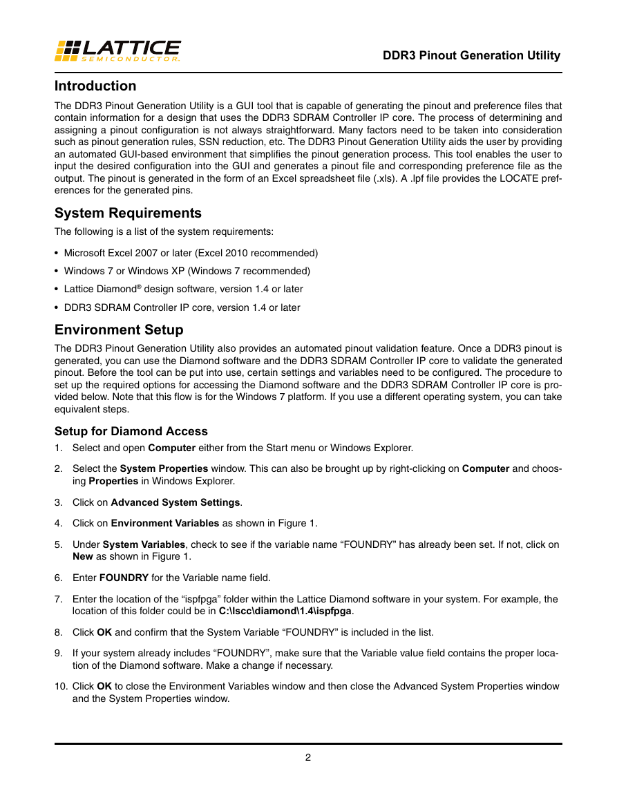
4. Click on Environment Variables as shown in Figure 1.
5. Under System Variables, check to see if the variable name “FOUNDRY” has already been set. If not, click on
New as shown in Figure 1.
6. Enter FOUNDRY for the Variable name field.
7. Enter the location of the “ispfpga” folder within the Lattice Diamond software in your system. For example, the
location of this folder could be in C:\lscc\diamond\1.4\ispfpga.
8. Click OK and confirm that the System Variable “FOUNDRY” is included in the list.
9.
If your system already includes “FOUNDRY”, make sure that the Variable value field contains the proper loca-
tion of the Diamond software. Make a change if necessary.
10. Click OK to close the Environment Variables window and then close the Advanced System Properties window
and the System Properties window.
2
�
Figure 1. Environment Variables
DDR3 Pinout Generation Utility
Setup for DDR3 SDRAM Controller IP Core Access
The DDR3 Pinout Generation Utility is by default configured to work with the DDR3 SDRAM Controller IP core ver-
sion 1.4 installed in the default folder. If you have a different version or have installed it in a different folder, then the
tool has to be configured as given below:
1. Click on the folder named Backend inside the DDR3_Pinout_Utility folder.
2. Open the IP_PATH.txt file.
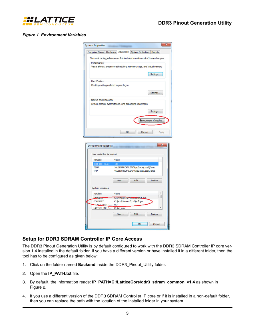
3. By default, the information reads: IP_PATH=C:/LatticeCore/ddr3_sdram_common_v1.4 as shown in
Figure 2.
4.
If you use a different version of the DDR3 SDRAM Controller IP core or if it is installed in a non-default folder,
then you can replace the path with the location of the installed folder in your system.
3
�
5. Save the file and close.
Figure 2. IP_PATH File Default Contents
DDR3 Pinout Generation Utility
Installation and Execution
The DDR3 Pinout Generation Utility is available for download in a .zip file format. Various tools like WinZip, WinRar
or 7-Zip can be used to extract the files into a folder. The zip file can be extracted to any folder. Once the extraction
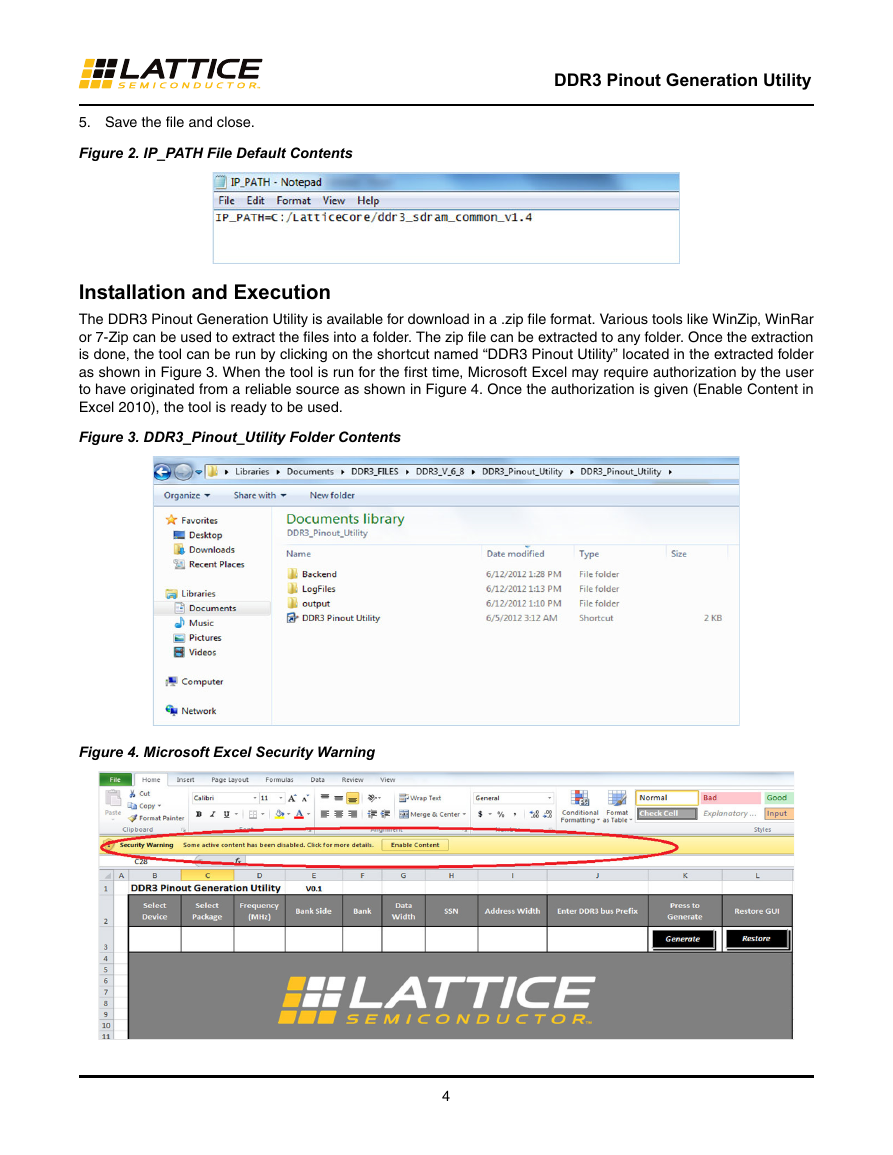
is done, the tool can be run by clicking on the shortcut named “DDR3 Pinout Utility” located in the extracted folder
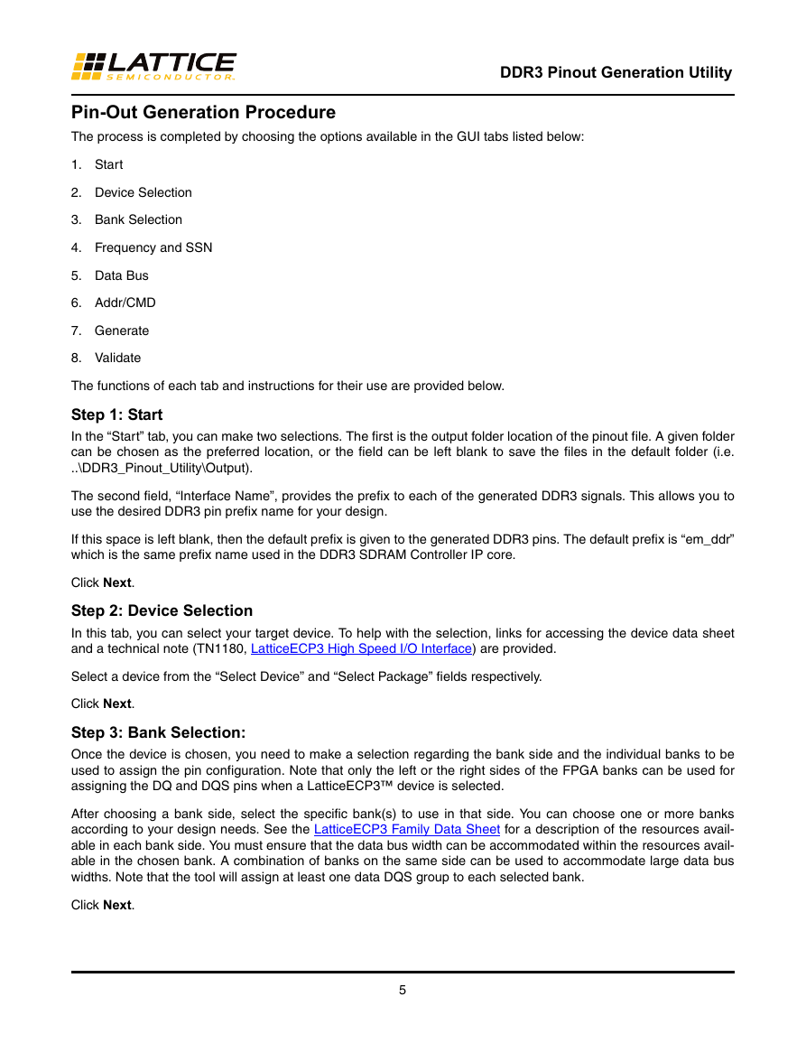
as shown in Figure 3. When the tool is run for the first time, Microsoft Excel may require authorization by the user
to have originated from a reliable source as shown in Figure 4. Once the authorization is given (Enable Content in
Excel 2010), the tool is ready to be used.
Figure 3. DDR3_Pinout_Utility Folder Contents
Figure 4. Microsoft Excel Security Warning
4
�
Pin-Out Generation Procedure
The process is completed by choosing the options available in the GUI tabs listed below:
DDR3 Pinout Generation Utility
1. Start
2. Device Selection
3. Bank Selection
4. Frequency and SSN
5. Data Bus
6. Addr/CMD
7. Generate
8. Validate
The functions of each tab and instructions for their use are provided below.
Step 1: Start
In the “Start” tab, you can make two selections. The first is the output folder location of the pinout file. A given folder
can be chosen as the preferred location, or the field can be left blank to save the files in the default folder (i.e.
..\DDR3_Pinout_Utility\Output).
The second field, “Interface Name”, provides the prefix to each of the generated DDR3 signals. This allows you to
use the desired DDR3 pin prefix name for your design.
If this space is left blank, then the default prefix is given to the generated DDR3 pins. The default prefix is “em_ddr”
which is the same prefix name used in the DDR3 SDRAM Controller IP core.
Click Next.
Step 2: Device Selection
In this tab, you can select your target device. To help with the selection, links for accessing the device data sheet
and a technical note (TN1180, LatticeECP3 High Speed I/O Interface) are provided.
Select a device from the “Select Device” and “Select Package” fields respectively.
Click Next.
Step 3: Bank Selection:
Once the device is chosen, you need to make a selection regarding the bank side and the individual banks to be
used to assign the pin configuration. Note that only the left or the right sides of the FPGA banks can be used for
assigning the DQ and DQS pins when a LatticeECP3™ device is selected.
After choosing a bank side, select the specific bank(s) to use in that side. You can choose one or more banks
according to your design needs. See the LatticeECP3 Family Data Sheet for a description of the resources avail-
able in each bank side. You must ensure that the data bus width can be accommodated within the resources avail-
able in the chosen bank. A combination of banks on the same side can be used to accommodate large data bus
widths. Note that the tool will assign at least one data DQS group to each selected bank.
Click Next.
5
�
DDR3 Pinout Generation Utility
Step 4: Frequency and SSN
In this tab, the user chooses the design frequency. The speed grade performance and device selection options are
as follows:
A 400 MHz design requires a -8 speed grade device and requires CK to be placed only in the left or right banks
A 333 MHz design requires a -8 or -7 speed grade device
A 300 MHz design is supported by all the given devices
The next selection in this tab addresses the SSN (Simultaneous Switching Noise) reduction of the design. Refer-
ence TN1180, LatticeECP3 High Speed I/O Interface for specifics on SSN reduction. A link to this technical note is
also provided in the “Device Selection” tab.
For SSN reduction, there are three settings to choose from: Best, Allowed and Off.
Best – Provides the highest reduction of SSN, but may require extra resources for implementation.
Allowed – Considers the reduction of SSN and provides the optimal pin resource utilization. This option is rec-
ommended for general DDR3 pinout generation.
Off – Does not allow any consideration for SSN reduction and is generally not recommended.
Click Next.
Step 5: Data Bus
This option is used to select the memory-side data bus width. The selection must be made in accordance with the
bank selections for the design.
Also available in this tab is the option for the user to manually choose the DQS locations. You can manually locate
the DQS pads if you have already determined the DQS groups to be used for data implementation by going
through the guidelines. The DDR3 Pinout Generation Utility will take care of only the rest of the DDR3 interface sig-
nals. Once a data bus width is determined and the Manual DQS selection option is selected, you can manually
assign each DQS pin to a valid DQS location available from the pull-down list for each group. It is recommended
that the Manual DQS selection option remain unchecked the first time a pinout is run so that the tool can provide
the best possible pinout that utilizes the maximum resources.
Click Next.
Step 6: ADDR/CMD
This tab is used to define the width of the address bus and the allowed location of the address and command pads.
Below are the instructions for placement of the non-data DDR3 pins:
The allowed range of the address width is from 13 to 16 bits following the DDR3 SDRAM Controller IP core spec-
ification.
By default, the DDR3 Pinout Generation Utility places the address bus on the same bank side as the DQ assign-
ment. If there are not enough pin resources available on this side, you can enable the top side banks to be used
for the address, command and control signals by selecting the Allow Top Side Bank option.
If the DDR3 memory configuration supports dual rank, the Dual Rank Support option should be selected to
include the pins for the second rank signals (CS, ODT, CK and CKE) to the generated pinout list.
The tool allows you to generate another set of CK pairs for each rank (for signal integrity purposes), following the
IP core’s CK pair duplication feature.
Click Next.
6
�
DDR3 Pinout Generation Utility
Step 7: Generate
At this point, the tool is ready to generate the configured DDR3 pinout. Click Generate to generate the pinout file.
There are two output windows.
The Output File log window provides information on whether the pinout generation has been successfully com-
pleted. It also displays the location of the generated pinout file.
The Quick Reference Log window provides a summary of the assigned DQS pads, reference clock pad, DDR3
clock pad and bank information. This information can be useful to generate the DDR3 SDRAM Controller IP core
configuration that corresponds to the pinout generated by this tool.
Go to the output folder and open the generated spreadsheet file. The pinout file is color-coded to help differentiate
between different pin groups. The grey colored cells are fixed and cannot be moved to any other location. You may
find a few cells that are color-coded but left blank without any information. This provides you the option to refine the
DDR3 pinout for your design needs. For example, you can move the location of an assigned address pin to a blank
cell that is coded in the same color or exchange pins between the same color-coded locations.
If there is a problem in generation, an error message is generated with suggested changes.
You can proceed to validation by pressing Next.
Step 8: Validate
Click Validate to validate the generated DDR3 pinout. The validation process checks whether the generated DDR3
pinout is legal by processing the pinout using the DDR3 SDRAM Controller IP core and Diamond software. It also
confirms that the generated pinout is able to meet the static timing requirements using the DDR3 SDRAM Control-
ler IP core test configuration.
Below are the steps that take place during the pinout validation process:
1. A DDR3 SDRAM Controller IP core is generated by the DDR3 Pinout Generation Utility using the pinout config-
uration information provided by the user.
2. The LOCATE preferences from the generated LPF are transferred to the validation project in the generated IP
core.
3. Diamond software is opened by the DDR3 Pinout Generation Utility.
4. The tool processes the validation project using the Diamond software.
5. Several output files providing information on pin legality and timing closure results are created and saved to the
Logfiles folder. The generated files include the consolidated preference file (.lpf), the mapper (.mrp) and place
& route report (.par) files, the pad report (.pad) and the static timing report (.twr) files. Note: These output files
are available for only one pinout configuration at a time. When a new pinout is validated, these files are over-
written. If you wish to keep these files, create a back-up by copying them into another folder/location before
running validation for a new pinout configuration.
You can use the generated output files to confirm the validation of the generated DDR3 pinout. Note that the
consolidated LPF file in the Logfiles folder is a good starting point for your project because it includes all neces-
sary preferences for using the DDR3 SDRAM Controller IP core with the generated pinout.
Note:
• When Validate is pressed, it consumes any related .lpf files that have been generated. To validate the same con-
figuration again, you need to generate the ,lpf files again before validation.
• The DDR3 Pinout Generation Utility runs on Microsoft Excel and when you close the utility, it automatically
closes any other Excel pages that may be running on your system. Ensure that you save and close any other
Excel spreadsheets before you run the tool to ensure no loss of information.
7
�
DDR3 Pinout Generation Utility
Technical Support Assistance
Hotline: 1-800-LATTICE (North America)
+1-503-268-8001 (Outside North America)
techsupport@latticesemi.com
e-mail:
Internet: www.latticesemi.com
Revision History
Date
June 2012
Version
01.0
Initial release.
Change Summary
© 2012 Lattice Semiconductor Corp. All Lattice trademarks, registered trademarks, patents, and disclaimers are as
listed at www.latticesemi.com/legal. All other brand or product names are trademarks or registered trademarks of
their respective holders. The specifications and information herein are subject to change without notice.
8
�



 2023年江西萍乡中考道德与法治真题及答案.doc
 2012年重庆南川中考生物真题及答案.doc
 2013年江西师范大学地理学综合及文艺理论基础考研真题.doc
 2020年四川甘孜小升初语文真题及答案I卷.doc
 2020年注册岩土工程师专业基础考试真题及答案.doc
 2023-2024学年福建省厦门市九年级上学期数学月考试题及答案.doc
 2021-2022学年辽宁省沈阳市大东区九年级上学期语文期末试题及答案.doc
 2022-2023学年北京东城区初三第一学期物理期末试卷及答案.doc
 2018上半年江西教师资格初中地理学科知识与教学能力真题及答案.doc
 2012年河北国家公务员申论考试真题及答案-省级.doc
 2020-2021学年江苏省扬州市江都区邵樊片九年级上学期数学第一次质量检测试题及答案.doc
 2022下半年黑龙江教师资格证中学综合素质真题及答案.doc