1. Revision History……………………………………………………………………………..2
2. Contents……………………………………………………………………………………….3
3.
General Description
……………………………………………………………………….4
4. Absolute Maximum Ratings……………………………………………………………..5
5. Electrical Specification…………………………………………………………………….6
6. Optical Specification……………………………………………………………………….8
7. Viewing Modes……………………………………………………………………………….8
8. Outline Dimension………………………………………………………………………….11
9. Block Diagram……………………………………………………………………………….13
10. INTERFACE …………………………………………………….……………………………13
11. Command/AC Timing………..………………………………..………………………… 15
12. Handling Precautions…………………………………….……………………………..18
�
3. General Description
3.1 Description
FORMIKE KWH101FL06-F01 is a TFT active matrix electrophoretic display, color active matrix TFT (Thin
Film Transistor) liquid crystal display (LCD) that uses amorphous silicon TFT as a switching device. This
model is composed of a TFT-LCD module, a driver circuit and a back-light unit. Graphics and texts can be
displayed on 1024 (W) x 3 x600 (H) dots with LVDS data signal. The following table described the features of
FORMIKE KWH101FL06-F01
3.2 Application
Portable DVD
GPS
Notebook
3.3 Advantage
High Resolution: WSVGA 1024(RGB) x 600 Dots
3.3V LVDS (Low Voltage Differential Signaling) interface with 1 pixel/clock
adopting a high aperture ratio
Dot-Inversion
3.4 Features
Feature
Size
Driver element
Display mode
Display Resolution
Active area
Dot pitch
Outline Dimension (W x H x D)
Luminance
constrast ratio
Surface treatment
Color Arrangement
interface
View Direction
Module weight
Description
10.1 inchs (16:9 Diagonal)
a-Si TFT active matrix
Normally White, transmissive
1024x 600 (H x V)
222.72 x 125.28 mm
0.2175 (W) x 0.2088(H)
235 x 143 x 5.15mm
200cd/m2 (Typ.)
500
Anti-Glare,
RGB stripe
LVDS
12 o'clock
TBD
NOTE: about Viewing Direction, the best viewing direction is 12 o’clock, and the optimum contrast direction is at
6 o’clock.
�
Item
4. ABSOLUTE MAXIMUM RATINGS
Min.
-0.3
-0.3
-0.3
Power Voltage
Power Voltage
Logic Output
Symbol
VDD,
Vin
VOUT
Condition
GND=0
GND=0
GND=0
Max.
4
VDD+0.3
VDD+0.3
Voltage
Storage Temperature(Ambient)
Operation Temperature(Ambient)
TSTG
TOPR
-20
0
+60
+50
Unit
V
V
V
°C
°C
Remark
NOTE
NOTE
Note: Device is subject to be damaged permanently if stresses beyond those absolute maximum
ratings listed above
1. Temp. _ 60, 90% RH MAX_ .
Temp. _ 60_, Absolute humidity shall be less than 90% RH at 60_
2.
�
5. ELECTRICAL SPECIFICATIONS(Ta=25°C)
5.1. Operating conditions: Ta = 25 ± 2 ºC
Item
Power Supply Voltage
LVDS Differential Input
High Threshold
LVDS Differential Input
Low Threshold
LVDS Common Mode
Voltage
LVDS Differential Input
Voltage
Terminating Resistor
Symbol
DVDD
VTH(LVDS)
VTL(LVDS)
VCM
|VID|
Values
Typ.
3.3
-
-
-
-
Min.
3
-
-100
1.125
100
Max.
3.6
+100
-
1.375
600
Unit
Remark
V
mV
mV
V
mV
Note2
Note 2
Note 2
Note 2
Ohm
-
Note 1: The ambient temperature is Ta = 25 ± 2 ºC.
Note 2:The parameters of LVDS signals are defined as the following figures.
100
RT
-
0V
VCM
VTH(LVDS)
Differential
Single Ended
5.2. Backlight Driving Section
Item
LED Voltage
LED Current
Power Consumption
Life Time
Note 1: There are 1 Groups LED
Note 2: The ambient temperature is Ta = 25 ± 2 ºC.
Note 3: Brightness to be decreased to 50% of the initial valu
e
Min.
4.8
-
-
-
0V
VTL(LVDS)
Symbol
LED-VDD
5
180
(25,000)
Typ.
IL
PLED
-
Max.
5.5
-
-
|VID|
|VID|
Unit
V
mA
mW
hr
Remark
Note 1
Note2;3
�
5.3.RECOMMENDED OPERATING RATINGS
Parameter
Symbol
EN Control Level
PWM Control Level
Backlight on
Backlight off
PWM High Level
PWM Low Level
PWM Control Duty Ratio
PWM Control Permissive Ripple
Voltage
PWM Control Frequency
VPWM_pp
fPWM
Min.
1.8
0
1.3
0
20
200
Value
Typ.
Max.
Unit
Note
-
-
-
-
400
5
0.8
5
0.15
100
100
500
V
V
V
V
%
mV
Hz
5.4 LED BACKLIGHT CONTROLL ON/OFF SEQUENCE
Power Off
Power On
TA
TB
LED_VDD
0V
LED_PWM 0V
LED_EN
0V
TC
TD
Timing Specifications:
TA ≧ 0ms
TB ≧ 0ms
TC ≧ 10ms
TD ≧ 0ms
Note (1) Please follow the LED backlight power sequence as above. If the customer
could not follow, it might cause backlight flash issue during display
ON/OFF or damage the LED backlight controller
�
Contrast Ratio
Brightness
Brightness Uniformity
C/R
Response Time
Color
WHITE
Coordinate
view angle
Min.
150
-
-
-
0.28
0.29
-
-
-
-
6.2
Tr+Tf
Wx
Wy
θl
θr
θu
θd
TR
Transmittance Ratio
Note:
1. Contrast Ratio(CR) is defined mathematically as :
Typ.
500
200
80%
8
0.31
0.34
60
60
50
55
6.6
-
-
-
-
0.35
0.38
-
-
-
-
6.68
cd/m2
%
ms
Degree
%
Remarks
Fig.1
Full White Pattern
Full White Pattern Fig.1,2
Fig.3
IBL=20mA
Full White Pattern
Fig.4
Center
(C/R>10)
LCD With POL
6. OPTICAL SPECIFICATIONS(Ta=25℃)
Unit
Symbol
Item
Max.
Contrast Ratio =
Surface Luminance with all white pixels
Surface Luminance with all black pixels
2. Surface luminance is the center point across the LCD surface 500mm from the surface with all
pixels displaying white. For more information see FIG 1.
3. Response time is the time required for the display to transition from black to white (Rise Time, Tr) and from white to
black(Decay Time, Tf). For additional information see FIG 3.
4. Viewing angle is the angle at which the contrast ratio is greater than 5. The angles are determined for the horizontal
or x axis and the vertical or y axis with respect to the z axis which is normal to the LCD surface. For more information
see FIG 4.
5. Optimum contrast is obtained by adjusting the LCD Threshold voltage (Vth& Vsat)
7. Viewing Modes
�
P1-P9:
�
Test equipment setup:
After stabilizing and leaving the panel alone at a driven temperature for 10 minutes, the
FIG.4 The definition of Viewing Angle
�


 V2版本原理图(Capacitive-Fingerprint-Reader-Schematic_V2).pdf
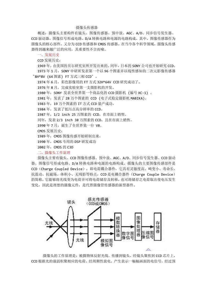 摄像头工作原理.doc
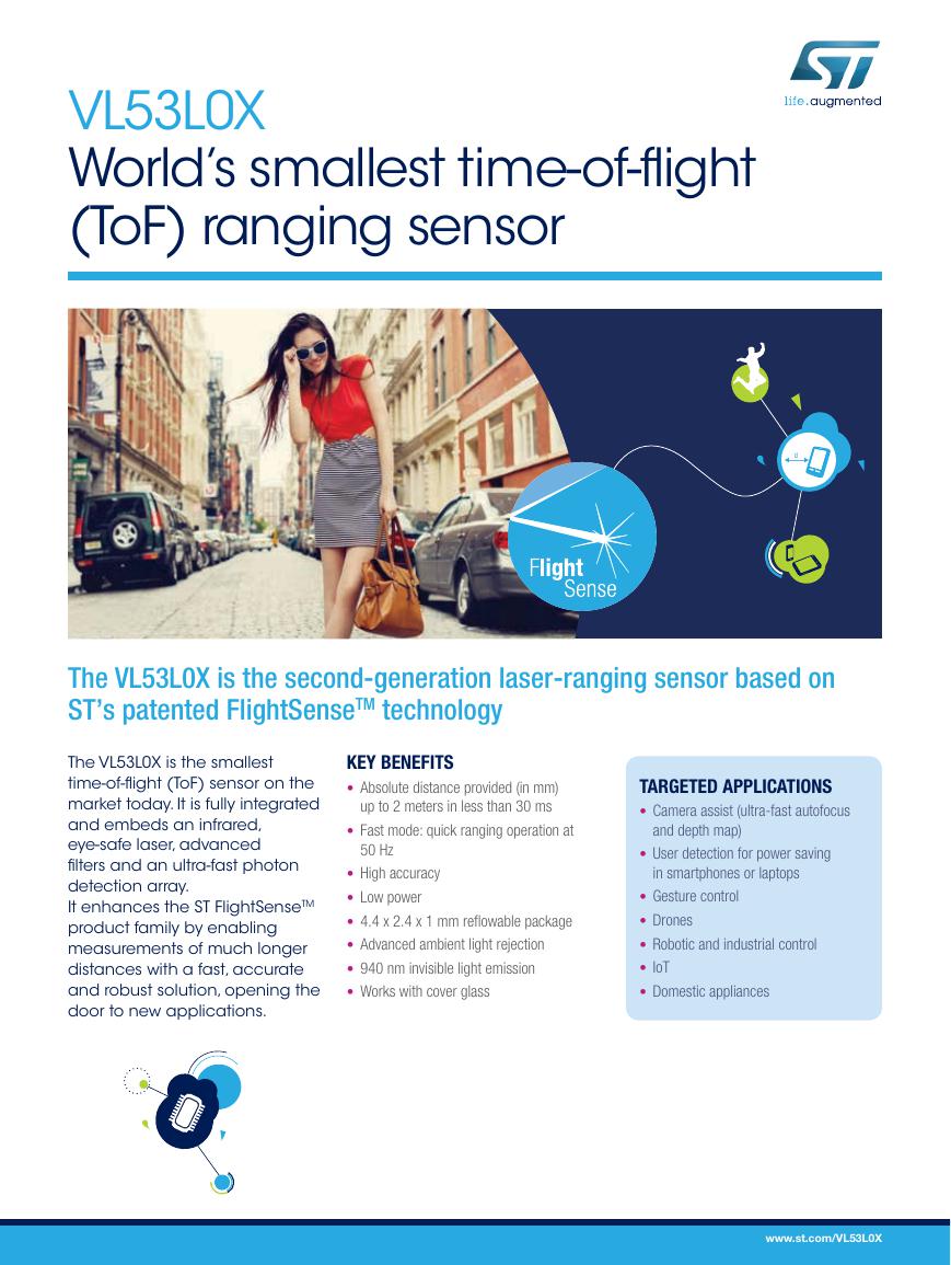 VL53L0X简要说明(En.FLVL53L00216).pdf
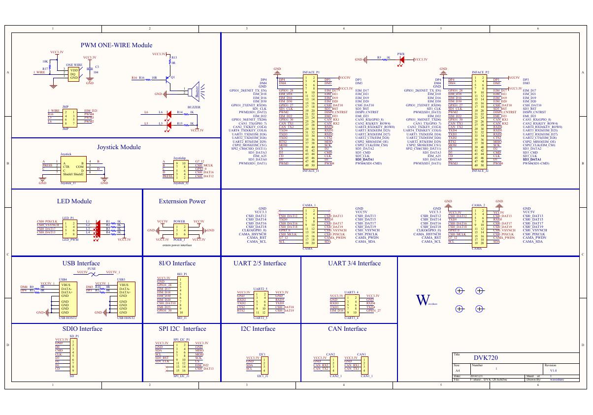 原理图(DVK720-Schematic).pdf
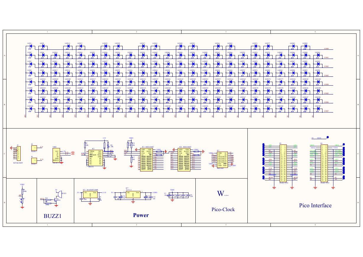 原理图(Pico-Clock-Green-Schdoc).pdf
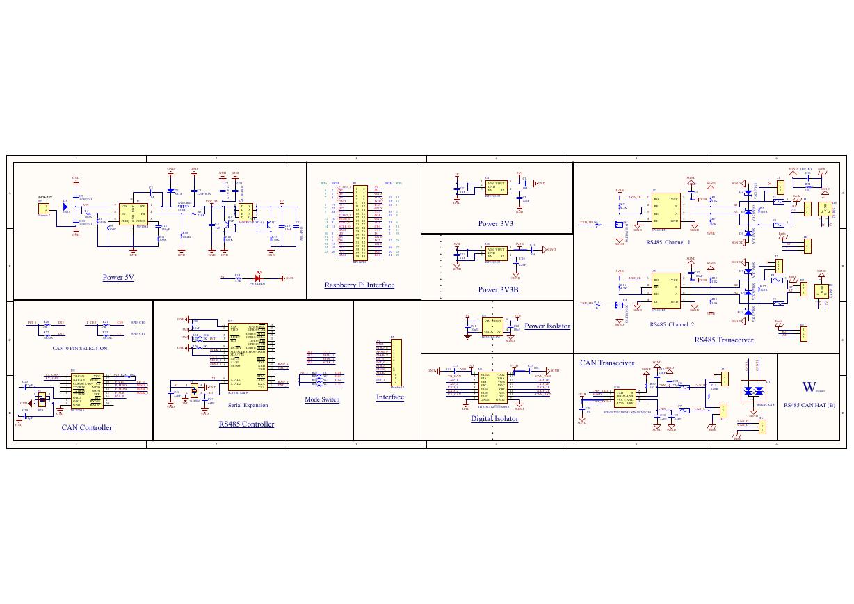 原理图(RS485-CAN-HAT-B-schematic).pdf
 File:SIM7500_SIM7600_SIM7800 Series_SSL_Application Note_V2.00.pdf
 ADS1263(Ads1262).pdf
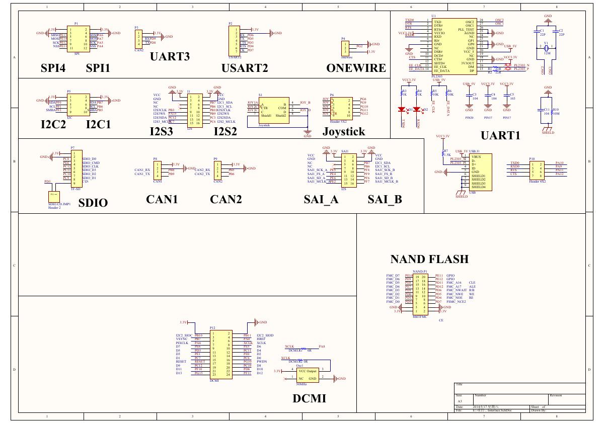 原理图(Open429Z-D-Schematic).pdf
 用户手册(Capacitive_Fingerprint_Reader_User_Manual_CN).pdf
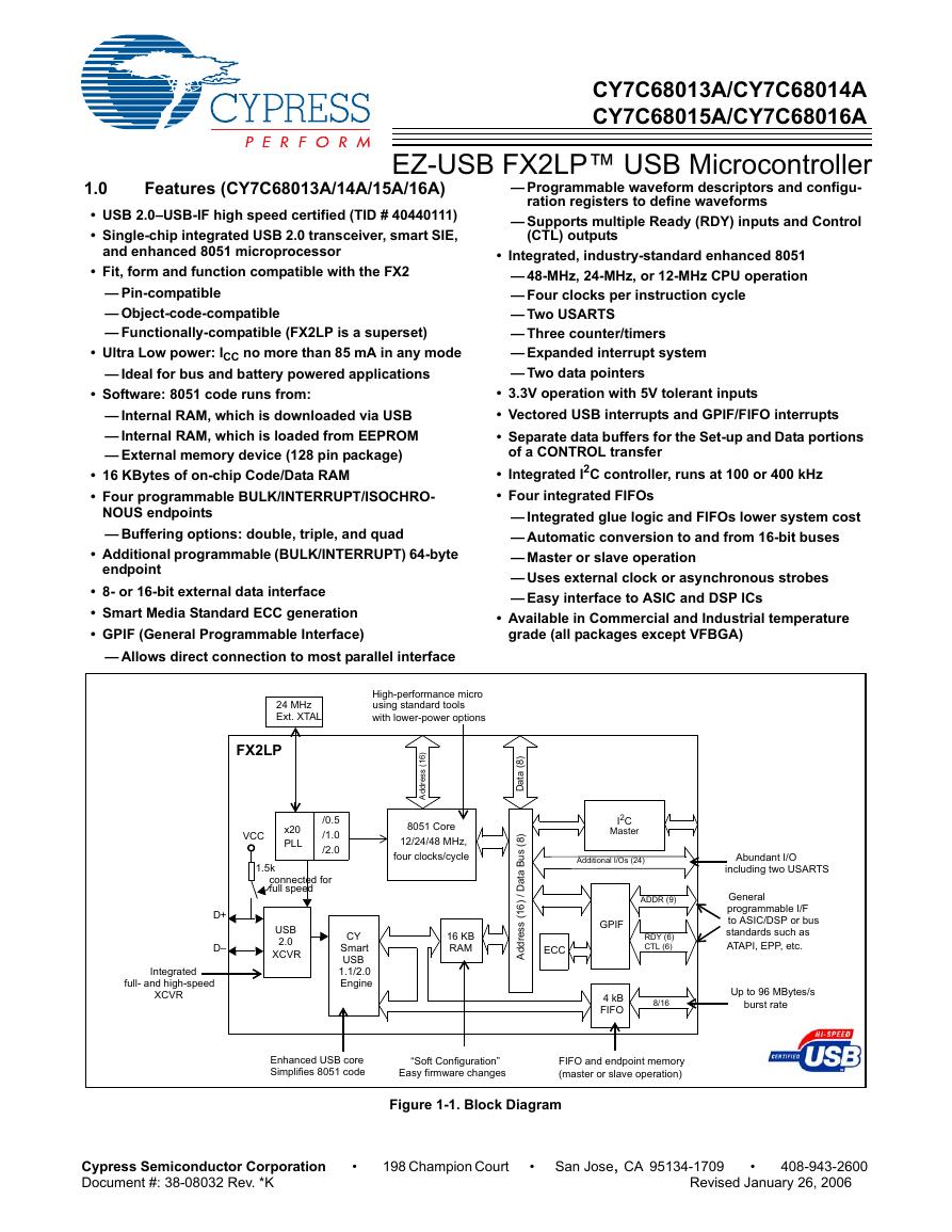 CY7C68013A(英文版)(CY7C68013A).pdf
 TechnicalReference_Dem.pdf