Hitachi Displays
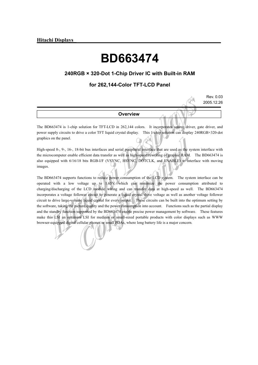
BD663474
240RGB × 320-Dot 1-Chip Driver IC with Built-in RAM
for 262,144-Color TFT-LCD Panel
Rev. 0.03
2005.12.26
Overview
The BD663474 is 1-chip solution for TFT-LCD in 262,144 colors. It incorporates source driver, gate driver, and
power supply circuits to drive a color TFT liquid crystal display. This 1-chip solution can display 240RGB×320-dot
graphics on the panel.
High-speed 8-, 9-, 16-, 18-bit bus interfaces and serial peripheral interface that are used as the system interface with
the microcomputer enable efficient data transfer as well as high-speed rewriting of graphic RAM. The BD663474 is
also equipped with 6/16/18 bits RGB-I/F (VSYNC, HSYNC, DOTCLK, and ENABLE) to interface with moving
images.
low voltage up
to 1.65V, which can minimize
The BD663474 supports functions to reduce power consumption of the LCD system. The system interface can be
operated with a
to
charging/discharging of the LCD module wiring and can transfer data at high-speed as well. The BD663474
incorporates a voltage follower circuit to generate a liquid crystal drive voltage as well as another voltage follower
circuit to drive large-volume liquid crystal for every output. These circuits can be built into the optimum setting by
the software, taking the picture quality and the power consumption into account. Functions such as the partial display
and the standby function supported by the BD663474 enable precise power management by software. These features
make this LSI an optimum LSI for medium or small-sized portable products with color displays such as WWW
browser-equipped digital cellular phones or small PDAs, where long battery life is a major concern.
the power consumption attributed
�
BD663474
Hitachi Displays
Features
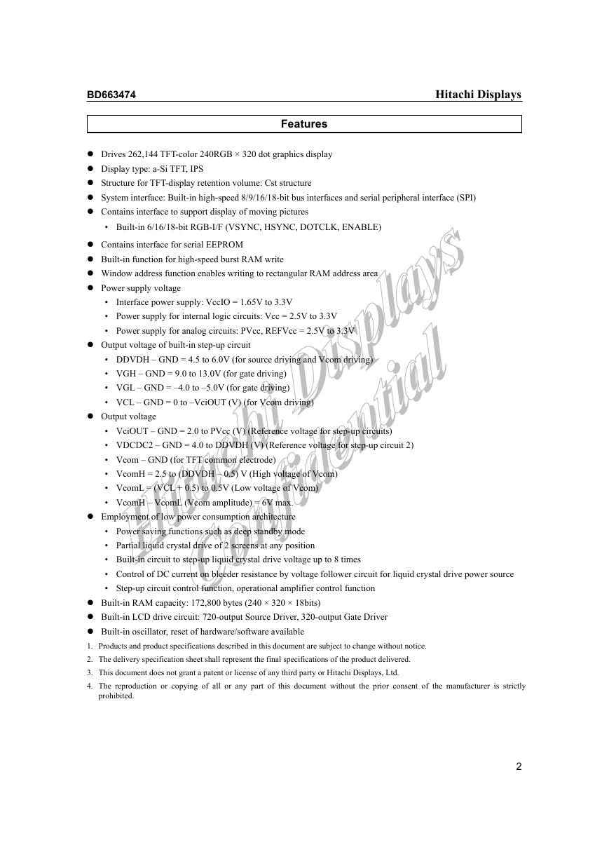
Drives 262,144 TFT-color 240RGB × 320 dot graphics display
Display type: a-Si TFT, IPS
Structure for TFT-display retention volume: Cst structure
System interface: Built-in high-speed 8/9/16/18-bit bus interfaces and serial peripheral interface (SPI)
Contains interface to support display of moving pictures
• Built-in 6/16/18-bit RGB-I/F (VSYNC, HSYNC, DOTCLK, ENABLE)
Contains interface for serial EEPROM
Built-in function for high-speed burst RAM write
Window address function enables writing to rectangular RAM address area
Power supply voltage
• Interface power supply: VccIO = 1.65V to 3.3V
• Power supply for internal logic circuits: Vcc = 2.5V to 3.3V
• Power supply for analog circuits: PVcc, REFVcc = 2.5V to 3.3V
Output voltage of built-in step-up circuit
• DDVDH – GND = 4.5 to 6.0V (for source driving and Vcom driving)
• VGH – GND = 9.0 to 13.0V (for gate driving)
• VGL – GND = –4.0 to –5.0V (for gate driving)
• VCL – GND = 0 to –VciOUT (V) (for Vcom driving)
Output voltage
• VciOUT – GND = 2.0 to PVcc (V) (Reference voltage for step-up circuits)
• VDCDC2 – GND = 4.0 to DDVDH (V) (Reference voltage for step-up circuit 2)
• Vcom – GND (for TFT common electrode)
• VcomH = 2.5 to (DDVDH – 0.5) V (High voltage of Vcom)
• VcomL = (VCL + 0.5) to 0.5V (Low voltage of Vcom)
• VcomH – VcomL (Vcom amplitude) = 6V max.
Employment of low power consumption architecture
• Power saving functions such as deep standby mode
• Partial liquid crystal drive of 2 screens at any position
• Built-in circuit to step-up liquid crystal drive voltage up to 8 times
• Control of DC current on bleeder resistance by voltage follower circuit for liquid crystal drive power source
• Step-up circuit control function, operational amplifier control function
Built-in RAM capacity: 172,800 bytes (240 × 320 × 18bits)
Built-in LCD drive circuit: 720-output Source Driver, 320-output Gate Driver
Built-in oscillator, reset of hardware/software available
1. Products and product specifications described in this document are subject to change without notice.
2. The delivery specification sheet shall represent the final specifications of the product delivered.
3. This document does not grant a patent or license of any third party or Hitachi Displays, Ltd.
4. The reproduction or copying of all or any part of this document without the prior consent of the manufacturer is strictly
prohibited.
2
�
Hitachi Displays
BD663474
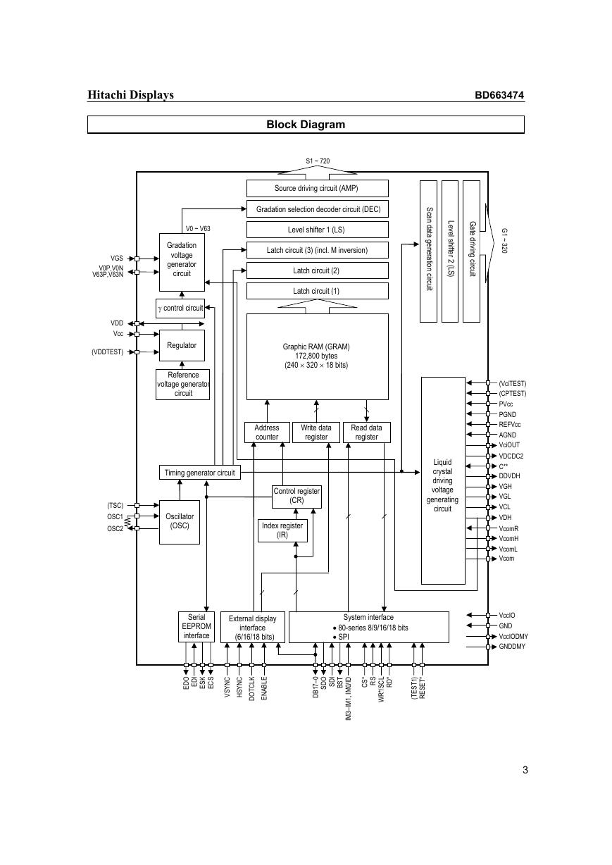
Block Diagram
S1 ~ 720
Source driving circuit (AMP)
Gradation selection decoder circuit (DEC)
V0 ~ V63
Level shifter 1 (LS)
VGS
V0P,V0N
V63P,V63N
VDD
Vcc
(VDDTEST)
Gradation
voltage
generator
circuit
γ control circuit
Regulator
Reference
voltage generator
circuit
Latch circuit (3) (incl. M inversion)
Latch circuit (2)
Latch circuit (1)
Graphic RAM (GRAM)
172,800 bytes
(240 × 320 × 18 bits)
t
S
c
a
n
d
a
a
g
e
n
e
r
a
t
i
o
n
c
i
r
c
u
i
t
L
e
v
e
l
s
h
i
f
t
e
r
2
(
L
S
)
Address
counter
Write data
register
Read data
register
Timing generator circuit
(TSC)
OSC1
OSC2
Oscillator
(OSC)
Control register
(CR)
Index register
(IR)
Liquid
crystal
driving
voltage
generating
circuit
Serial
EEPROM
interface
External display
interface
(6/16/18 bits)
System interface
• 80-series 8/9/16/18 bits
• SPI
O
D
E
I
D
E
K
S
E
S
C
E
C
N
Y
S
V
C
N
Y
S
H
K
L
C
T
O
D
E
L
B
A
N
E
*
S
C
S
R
*
D
R
L
C
S
/
*
R
W
)
1
T
S
E
T
(
*
T
E
S
E
R
O
D
S
I
D
S
T
S
B
0
–
7
1
B
D
D
I
/
0
M
I
,
I
1
M
–
3
M
I
G
1
~
3
2
0
G
a
e
t
i
d
r
i
v
n
g
c
i
r
c
u
i
t
(VciTEST)
(CPTEST)
PVcc
PGND
REFVcc
AGND
VciOUT
VDCDC2
C**
DDVDH
VGH
VGL
VCL
VDH
VcomR
VcomH
VcomL
Vcom
VccIO
GND
VccIODMY
GNDDMY
3
�
BD663474
Hitachi Displays
1. Control signals
Signal name
(Interface
voltage)
terminals
No. of
Input/
Output
Terminal Functions
Connected
to
Functions
RESET*
(VccIO/GND)
1
Input
External
reset circuit
Used to enter the hardware-reset signal.
Initializes LSI at “Low”.
Power-on reset is required when turning on power supply.
IM3-1,
IM0/ID
(VccIO/GND)
4
Input
GND
or
VccIO
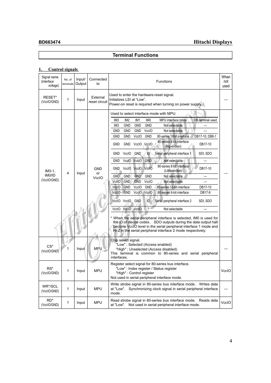
Used to select interface mode with MPU.
IM1
IM2
IM0
IM3
GND GND GND
IM3
GND GND GND VccIO
GND GND VccIO GND
GND GND VccIO VccIO
GND VccIO GND
ID
GND VccIO VccIO GND
GND VccIO VccIO VccIO
GND GND GND GND
VccIO GND GND VccIO
VccIO GND VccIO GND
VccIO GND VccIO VccIO
VccIO VccIO GND
VccIO VccIO VccIO
ID
*
MPU interface mode
DB terminal used
Not selectable
Not selectable
—
—
80-series 16bit interface
80-series 8-bit interface
(Big-endian)
DB17-10, DB8-1
DB17-10
Serial peripheral interface 1
SDI, SDO
Not selectable
80-series 8-bit interface
(Little-endian)
Not selectable
Not selectable
80-series 18-bit interface
80-series 9-bit interface
—
DB17-10
—
—
DB17-10
DB17-9
Serial peripheral interface 2
SDI, SDO
Not selectable
—
* When the serial peripheral interface is selected, IM0 is used for
the ID of device codes. SDO outputs during the data output halt
become VccIO level in the serial peripheral interface 1 mode and
Hi-Z in the serial peripheral interface 2 mode respectively.
When
not
used
—
—
CS*
(VccIO/GND)
RS*
(VccIO/GND)
WR*/SCL
(VccIO/GND)
RD*
(VccIO/GND)
1
1
1
1
Input
MPU
Input
MPU
Input
MPU
Input
MPU
Chip select signal.
"Low" : Selected (Access enabled)
"High" : Unselected (Access disabled)
This terminal is common to 80-series and serial peripheral
interfaces.
Register select signal for 80-series bus interface.
"Low" : Index register / Status register
"High" : Control register
Not used in serial peripheral interface mode.
Write strobe signal in 80-series bus interface mode. Writes data
at "Low". Synchronizing clock signal in serial peripheral interface
mode.
Read strobe signal in 80-series bus interface mode. Reads data
at "Low". Not used in serial peripheral interface mode.
—
VccIO
—
VccIO
4
�
Hitachi Displays
Signal name
(Interface
voltage)
No. of
terminals
Input/
Output
Connected
to
Functions
BD663474
DB17-0
(VccIO/GND)
18
Input/
Output
MPU
Input
MPU
Output
MPU
Input
MPU
Input
MPU
Input
MPU
Input
MPU
Output
MPU
Output EEPROM
SDI
(VccIO/GND)
SDO
(VccIO/GND)
VSYNC
(VccIO/GND)
HSYNC
(VccIO/GND)
DOTCLK
(VccIO/GND)
ENABLE
(VccIO/GND)
BST
(VccIO/GND)
ECS
(Vcc/GND)
ESK
(Vcc/GND)
EDI
(Vcc/GND)
EDO
(Vcc/GND)
1
1
1
1
1
1
1
1
1
1
1
18-bit bi-directional data bus in 80-series bus interface mode.
See below for terminals used in each mode.
8-bit interface
9-bit interface
16-bit interface : DB17-10, 8-1
: DB17-10
: DB17-9
18-bit interface : DB17-0
: DB17-12
18-bit RGB data bus in RGB interface mode. See below for
terminals used in each mode (RIM setting).
6-bit interface
16-bit interface : DB17-13, 11-1
18-bit interface : DB17-0
Fixed to "VccIO" or "GND" level when not used.
Serial data input terminal in serial peripheral interface mode.
Loads data on the rising edge of SCL. Fixed to "VccIO" or "GND"
level when not used.
Serial data output terminal in serial peripheral interface mode.
Outputs data on the falling edge of SCL.
Frame synchronization signal in RGB interface mode. This is a
"Low" active signal, but can be used as a "High" active signal by
changing the register setting. Set to inactive when the RGB
interface is not used.
Line synchronization signal in RGB interface mode. This is a
"Low" active signal, but can be used as a "High" active signal by
changing the register setting. Set to inactive when the RGB
interface is not used.
Dot clock signal in RGB interface mode. The timing of data
loading is set at the rising edge. This is a "High" active signal, but
can be used as a "Low" active signal by changing the register
setting. Set to inactive when the RGB interface is not used.
Data enable signal in RGB interface mode.
"Low" : Selected (Access enabled)
"High" : Unselected (Access disabled)
This is a "Low" active signal, but can be used as a "High" active
signal by changing the register setting. Set to inactive when the
interface is not used.
Outputs pulses indicating start of the blank period (front porch).
When writing data in synchronization with display scan, this can be
used as a trigger signal.
Chip select signal.
“High”: Selected (Access enabled)
“Low”: Unselected (Access disabled)
Output EEPROM Synchronizing clock signal.
Input
EEPROM Serial data input terminal. Loads data on the rising edge of ESK
signal. Fixed to “Vcc” or “GND” level when not used.
Output EEPROM Serial data output terminal. Outputs data on the falling edge of
ESK signal.
When
not
used
GND
or
VccIO
GND
or
VccIO
open
GND
or
VccIO
GND
or
VccIO
GND
or
VccIO
GND
or
VccIO
open
open
open
GND
or
Vcc
open
5
�
BD663474
Hitachi Displays
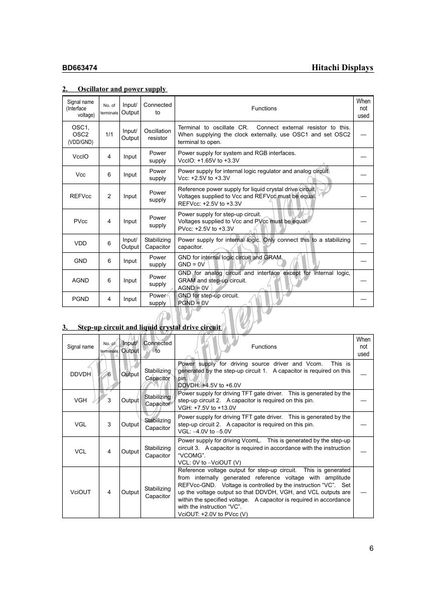
2. Oscillator and power supply
Signal name
(Interface
voltage)
Input/
Output
to
No. of
terminals
Connected
Functions
OSC1,
OSC2
(VDD/GND)
VccIO
Vcc
REFVcc
PVcc
VDD
GND
AGND
PGND
1/1
Input/
Output
Oscillation
resistor
4
6
2
4
6
6
6
4
Input
Input
Input
Input
Power
supply
Power
supply
Power
supply
Power
supply
Input/
Output
Stabilizing
Capacitor
Input
Input
Input
Power
supply
Power
supply
Power
supply
Terminal to oscillate CR. Connect external resistor to this.
When supplying the clock externally, use OSC1 and set OSC2
terminal to open.
Power supply for system and RGB interfaces.
VccIO: +1.65V to +3.3V
Power supply for internal logic regulator and analog circuit.
Vcc: +2.5V to +3.3V
Reference power supply for liquid crystal drive circuit.
Voltages supplied to Vcc and REFVcc must be equal.
REFVcc: +2.5V to +3.3V
Power supply for step-up circuit.
Voltages supplied to Vcc and PVcc must be equal.
PVcc: +2.5V to +3.3V
Power supply for internal logic. Only connect this to a stabilizing
capacitor.
GND for internal logic circuit and GRAM.
GND = 0V
GND for analog circuit and interface except for internal logic,
GRAM and step-up circuit.
AGND = 0V
GND for step-up circuit.
PGND = 0V
3. Step-up circuit and liquid crystal drive circuit
Signal name
No. of
terminals
Input/
Output
Connected
to
Functions
DDVDH
VGH
VGL
VCL
VciOUT
6
3
3
4
4
Output Stabilizing
Capacitor
Output Stabilizing
Capacitor
Output Stabilizing
Capacitor
Output Stabilizing
Capacitor
Output Stabilizing
Capacitor
Power supply for driving source driver and Vcom. This is
generated by the step-up circuit 1. A capacitor is required on this
pin.
DDVDH: +4.5V to +6.0V
Power supply for driving TFT gate driver. This is generated by the
step-up circuit 2. A capacitor is required on this pin.
VGH: +7.5V to +13.0V
Power supply for driving TFT gate driver. This is generated by the
step-up circuit 2. A capacitor is required on this pin.
VGL: −4.0V to −5.0V
Power supply for driving VcomL. This is generated by the step-up
circuit 3. A capacitor is required in accordance with the instruction
“VCOMG”.
VCL: 0V to −VciOUT (V)
Reference voltage output for step-up circuit. This is generated
from
internally generated reference voltage with amplitude
REFVcc-GND. Voltage is controlled by the instruction “VC”. Set
up the voltage output so that DDVDH, VGH, and VCL outputs are
within the specified voltage. A capacitor is required in accordance
with the instruction “VC”.
VciOUT: +2.0V to PVcc (V)
When
not
used
—
—
—
—
—
—
—
—
—
When
not
used
—
—
—
—
—
6
�
Hitachi Displays
BD663474
Signal name
No. of
terminals
Input/
Output
Connected
to
Functions
VDCDC2
2
Output Stabilizing
Capacitor
C11+, C11-
4/4
C1A+, C1A-
4/4
C21+, C21-
2/2
C22+, C22-
2/2
C31+, C31-
4/4
Input/
Output
Input/
Output
Input/
Output
Input/
Output
Input/
Output
Step-up
capacitor
Step-up
capacitor
Step-up
capacitor
Step-up
capacitor
Step-up
capacitor
VDH
Vcom
VcomH
VcomL
VcomR
VGS
1
4
4
4
1
1
Output Stabilizing
Capacitor
Output
TFT
common
electrode
Output Stabilizing
Capacitor
Output Stabilizing
Capacitor
Input
Input
Variable
resistor or
open
GND or
external
resistor
reference
voltage with
Reference voltage output for step-up circuit 2. This is generated
from internally generated reference voltage with amplitude
REFVcc-GND. Voltage is controlled by the instruction “VRD”.
Set up the voltage output so that VGH and VGL outputs are within
the specified voltage. A capacitor is required in accordance with
the instruction “APR”.
VDCDC2: +4.0V to DDVDH (V)
Used for built-in step-up circuit 1. Connect a capacitor between
these pins.
Used for built-in step-up circuit 1. Connect a capacitor between
these pins in accordance with the instruction “CA”.
Used for built-in step-up circuit 2. Connect a capacitor between
these pins.
Used for built-in step-up circuit 2. Connect a capacitor between
these pins in accordance with the instruction “BT”.
Used for built-in step-up circuit 3. Connect a capacitor between
these pins in accordance with the instruction “VCOMG”.
Reference voltage output. This is generated from internally
generated
amplitude REFVcc-
GND.Voltage is controlled by the instructions “VC” and “VRH”.
This output is used for:
(1) Source driver gradation reference voltage VDH
(2) VcomH level reference voltage
(3) Vcom amplitude reference voltage
A capacitor is required.
VDH = 3.0 to (DDVDH – 0.5) (V)
Output for TFT display common electrode. Output level ranges
between VcomH and VcomL. This output inverts the polarity of
the common electrode voltage. The cycle of polarity inversion is
set with the register.
Vcom high level output. Voltage value is adjusted with VcomR
pin. A capacitor is required on this pin.
VcomH = 2.5 to (DDVDH – 0.5) (V)
Vcom low level output. Voltage value is controlled by the
instruction “VDV”. Set up the voltage output so that Vcom
amplitude is within the specified voltage. A capacitor is required
in accordance with the register “VCOMG”.
VcomL = (VCL + 0.5) to 0.5 V
Reference voltage input for VcomH. Apply the variable resistor
between VDH and GND to generate the reference voltage.
Reference level for gradation voltage generator circuit. Connect
external variable resistor when adjusting the level panel by panel
with the source driver.
S1~S720
720 Output
LC panel
Signal lines to output voltage for applied liquid crystal.
G1~G320
320 Output
LC panel
Gate line output.
• TFT ON level: VGH
• TFT OFF level: VGL
When
not
used
—
—
open
—
open
open
—
—
—
—
open
—
open
open
7
�
BD663474
4. Others
Signal name
(Interface
voltage)
VccIODMY
GNDDMY
TESTD0
TESTD1
TEST1
(VccIO/GND)
VDDTEST
(VccIO/GND)
CPTEST
(VccIO/GND)
VciTEST
(VccIO/GND)
TSC
(VDD/GND)
OSC3
(VccIO/GND)
TS0 – TS8
(VccIO/GND)
TOUT1 – 3
(VccIO/GND)
RESO
VTEST
VMON
V0P, V63P
V0N, V63N
TESTA
TESTC
VAEP, VAEN
VGLDMY
No. of
terminals
Input/
Output
Connected
to
Functions
2
4
1
1
1
1
1
1
1
1
9
3
1
1
1
2
2
1
1
2
4
Output
Output
Input
terminal
Input
terminal
Outputs internal "VccIO" level. When adjacent input terminals are
fixed at "VccIO", short-circuit these terminals.
Outputs internal "GND" level. When adjacent input terminals are
fixed at "GND", short-circuit these terminals.
Output
open
Test pin. Set to open.
Output
open
Test pin. Set to open.
Input
GND
Test pin. Fix to "GND".
Input
GND
Test pin. Fix to "GND".
Input
GND
Test pin. Fix to "GND".
Input
GND
Test pin. Fix to "GND".
Input
GND
Test pin. Fix to "GND".
Output
open
Test pin. Set to open.
Output
open
Test pins. Set to open.
Output
open
Test pins. Set to open.
Output
open
Test pin. Set to open.
Output
open
Test pin. Set to open.
Output
open
Test pin. Set to open.
Input/
Output
Input/
Output
open
Test pins. Set to open.
open
Test pins. Set to open.
Output
open
Test pin. Set to open.
Output
open
Test pin. Set to open.
Output
open
Test pins. Set to open.
Output
open
Outputs internal “VGL” level.
Hitachi Displays
When
not
used
open
open
open
open
—
—
—
—
—
open
open
open
open
open
open
open
open
open
open
open
open
—
8
DMY1 – 18
18
—
—
Dummy pads.
�



 V2版本原理图(Capacitive-Fingerprint-Reader-Schematic_V2).pdf
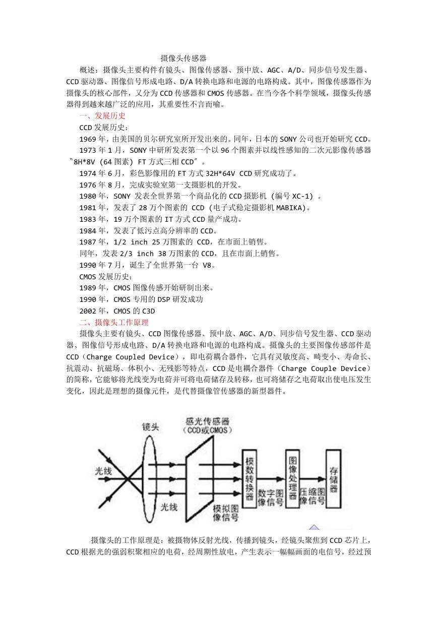 摄像头工作原理.doc
 VL53L0X简要说明(En.FLVL53L00216).pdf
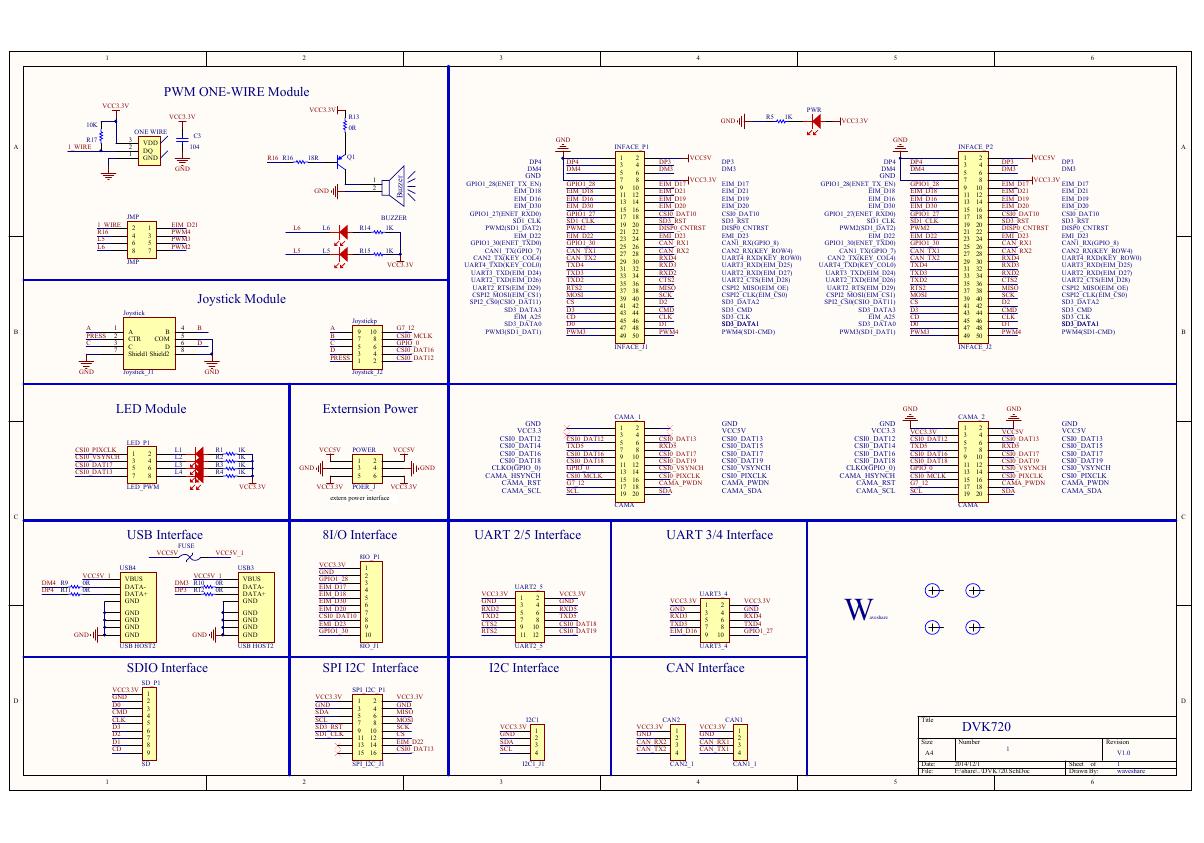 原理图(DVK720-Schematic).pdf
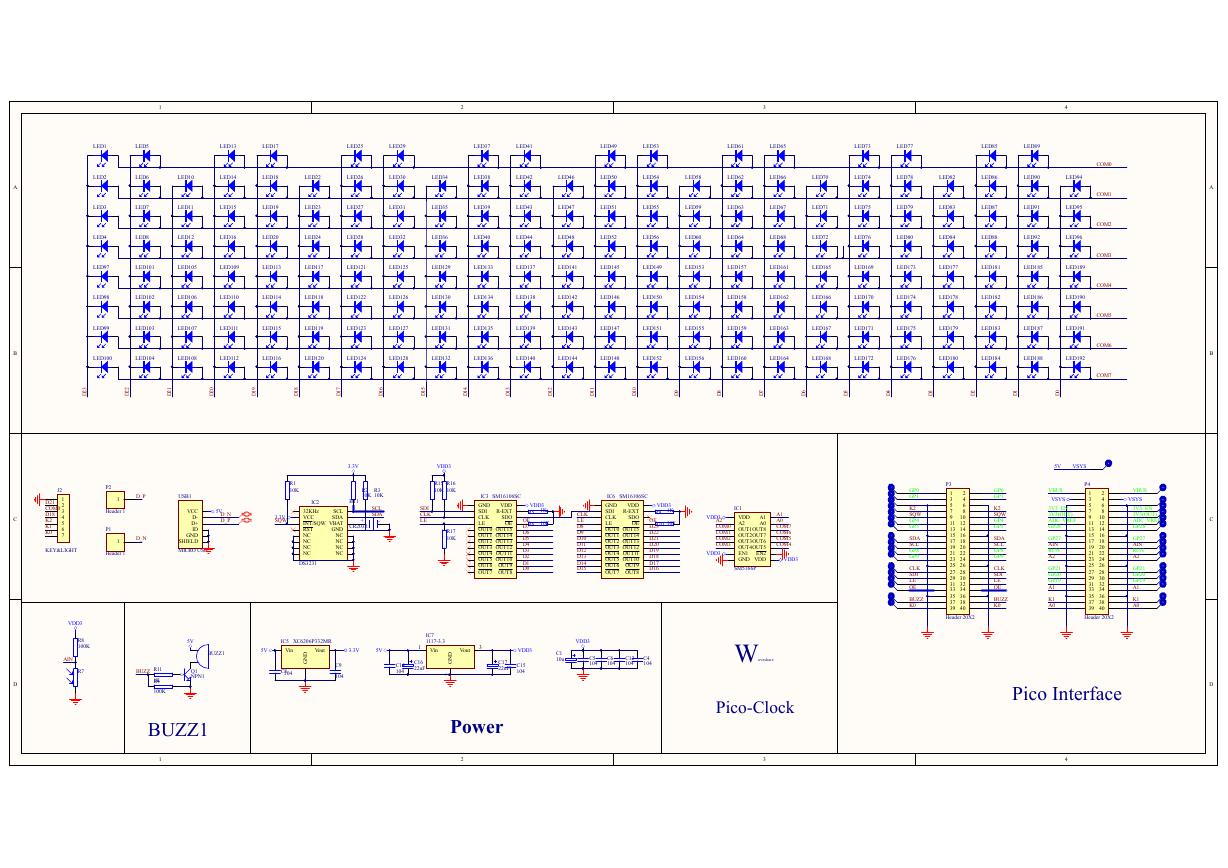 原理图(Pico-Clock-Green-Schdoc).pdf
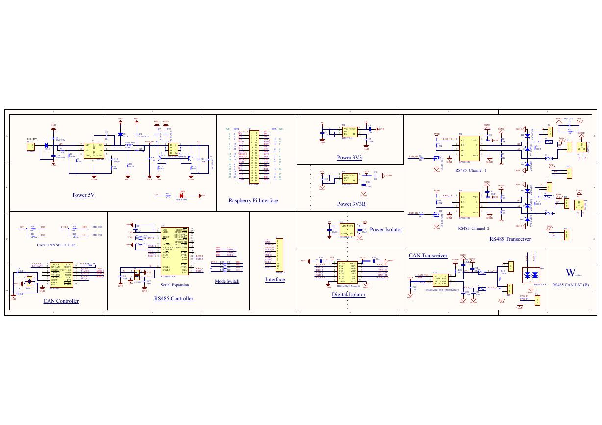 原理图(RS485-CAN-HAT-B-schematic).pdf
 File:SIM7500_SIM7600_SIM7800 Series_SSL_Application Note_V2.00.pdf
 ADS1263(Ads1262).pdf
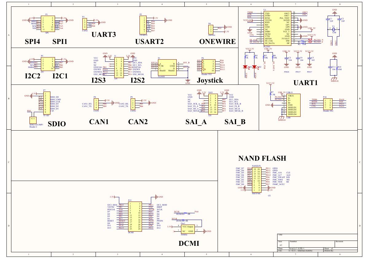 原理图(Open429Z-D-Schematic).pdf
 用户手册(Capacitive_Fingerprint_Reader_User_Manual_CN).pdf
 CY7C68013A(英文版)(CY7C68013A).pdf
 TechnicalReference_Dem.pdf