65KV2-CT
CHAPTER 1
INTRODUCTION
• This chapter briefly introduces the characteristics of this mainboard. It
includes the information regarding the chipset, CPU types, built-in
functions and layout. Users will have more ideas about mainboards after
reading this chapter.
THIS CHAPTER CONTAINS THE FOLLOWING TOPICS :
1-1 MAINBOARD SPECIFICATION
1-2 MAINBOARD LAYOUT
1-3 CHIPSET DIAGRAM
8
�
Chapter 1 Introduction
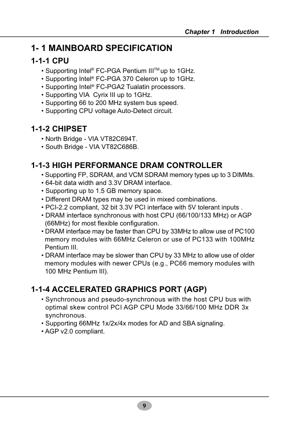
1- 1 MAINBOARD SPECIFICATION
1-1-1 CPU
• Supporting Intel® FC-PGA Pentium IIITM up to 1GHz.
• Supporting Intel® FC-PGA 370 Celeron up to 1GHz.
• Supporting Intel® FC-PGA2 Tualatin processors.
• Supporting VIA Cyrix III up to 1GHz.
• Supporting 66 to 200 MHz system bus speed.
• Supporting CPU voltage Auto-Detect circuit.
1-1-2 CHIPSET
• North Bridge - VIA VT82C694T.
• South Bridge - VIA VT82C686B.
1-1-3 HIGH PERFORMANCE DRAM CONTROLLER
• Supporting FP, SDRAM, and VCM SDRAM memory types up to 3 DIMMs.
• 64-bit data width and 3.3V DRAM interface.
• Supporting up to 1.5 GB memory space.
• Different DRAM types may be used in mixed combinations.
• PCI-2.2 compliant, 32 bit 3.3V PCI interface with 5V tolerant inputs .
• DRAM interface synchronous with host CPU (66/100/133 MHz) or AGP
(66MHz) for most flexible configuration.
• DRAM interface may be faster than CPU by 33MHz to allow use of PC100
memory modules with 66MHz Celeron or use of PC133 with 100MHz
Pentium III.
• DRAM interface may be slower than CPU by 33 MHz to allow use of older
memory modules with newer CPUs (e.g., PC66 memory modules with
100 MHz Pentium III).
1-1-4 ACCELERATED GRAPHICS PORT (AGP)
• Synchronous and pseudo-synchronous with the host CPU bus with
optimal skew control PCI AGP CPU Mode 33/66/100 MHz DDR 3x
synchronous.
• Supporting 66MHz 1x/2x/4x modes for AD and SBA signaling.
• AGP v2.0 compliant.
9
�
65KV2-CT
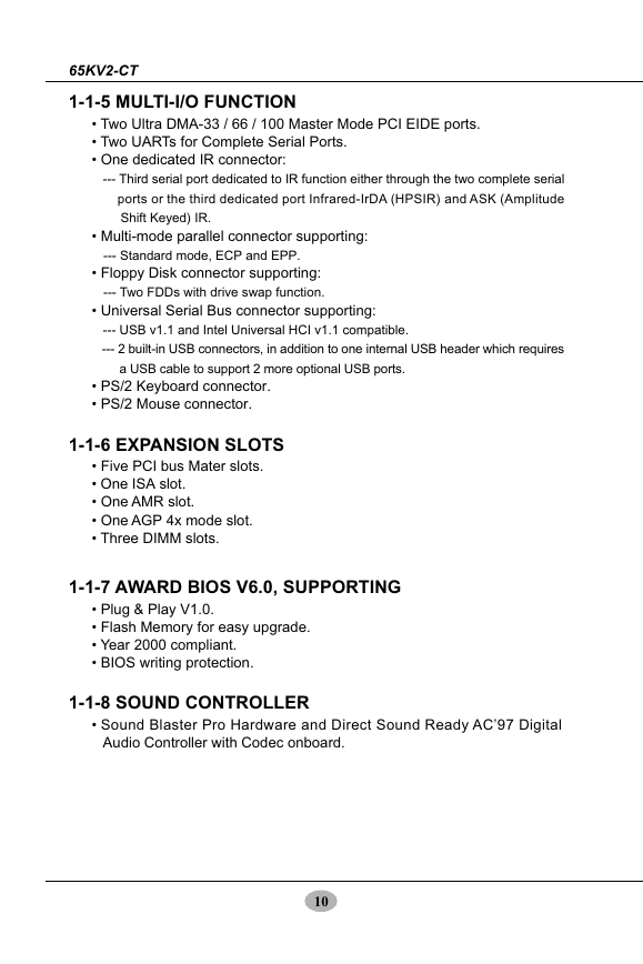
1-1-5 MULTI-I/O FUNCTION
• Two Ultra DMA-33 / 66 / 100 Master Mode PCI EIDE ports.
• Two UARTs for Complete Serial Ports.
• One dedicated IR connector:
--- Third serial port dedicated to IR function either through the two complete serial
ports or the third dedicated port Infrared-IrDA (HPSIR) and ASK (Amplitude
Shift Keyed) IR.
• Multi-mode parallel connector supporting:
--- Standard mode, ECP and EPP.
• Floppy Disk connector supporting:
--- Two FDDs with drive swap function.
• Universal Serial Bus connector supporting:
--- USB v1.1 and Intel Universal HCI v1.1 compatible.
--- 2 built-in USB connectors, in addition to one internal USB header which requires
a USB cable to support 2 more optional USB ports.
• PS/2 Keyboard connector.
• PS/2 Mouse connector.
1-1-6 EXPANSION SLOTS
• Five PCI bus Mater slots.
• One ISA slot.
• One AMR slot.
• One AGP 4x mode slot.
• Three DIMM slots.
1-1-7 AWARD BIOS V6.0, SUPPORTING
• Plug & Play V1.0.
• Flash Memory for easy upgrade.
• Year 2000 compliant.
• BIOS writing protection.
1-1-8 SOUND CONTROLLER
• Sound Blaster Pro Hardware and Direct Sound Ready AC’97 Digital
Audio Controller with Codec onboard.
10
�
Chapter 1 Introduction
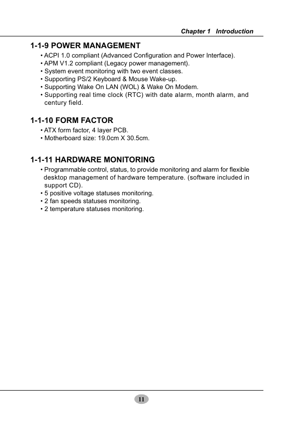
1-1-9 POWER MANAGEMENT
• ACPI 1.0 compliant (Advanced Configuration and Power Interface).
• APM V1.2 compliant (Legacy power management).
• System event monitoring with two event classes.
• Supporting PS/2 Keyboard & Mouse Wake-up.
• Supporting Wake On LAN (WOL) & Wake On Modem.
• Supporting real time clock (RTC) with date alarm, month alarm, and
century field.
1-1-10 FORM FACTOR
• ATX form factor, 4 layer PCB.
• Motherboard size: 19.0cm X 30.5cm.
1-1-11 HARDWARE MONITORING
• Programmable control, status, to provide monitoring and alarm for flexible
desktop management of hardware temperature. (software included in
support CD).
• 5 positive voltage statuses monitoring.
• 2 fan speeds statuses monitoring.
• 2 temperature statuses monitoring.
11
�
65KV2-CT
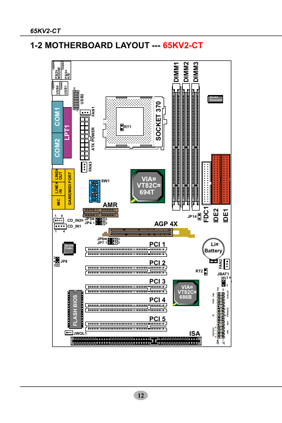
1-2 MOTHERBOARD LAYOUT --- 65KV2-CT
1
M
M
D
I
2
M
M
D
I
3
M
M
D
I
Clock
Generator
r
e
p
p
u
E
S
U
O
M
2
S
P
/
r
e
w
o
l
/
2
S
P
B
K
/
r
e
p
p
u
r
e
w
o
l
0
B
S
U
1
B
S
U
1
T
P
L
T
R
O
P
I
I
/
D
M
E
M
A
G
1
M
O
C
2
M
O
C
E
N
L
I
T
U
O
E
N
L
I
N
I
I
C
M
1 4
1 4
6
1
2
B
S
U
1
1
N
A
F
R
E
W
O
P
X
T
A
3
N
A
F
I
P
D
N
O
0
7
3
T
E
K
C
O
S
RT1
VIA
VT82C
694T
SW1
8
7
6
5
4
3
2
1
AMR
CD_IN2
CD_IN1
JP3
JP4
1 3
1 3
AGP 4X
JP6
JP7
1 3
1 3
AC'97
Codec
3
1
JP8
I
S
O
B
H
S
A
L
F
PCI 1
PCI 2
PCI 3
PCI 4
PCI 5
JWOL1
ISA
JP14
1
C
D
F
2
E
D
I
1
E
D
I
Li
Battery
2
N
A
F
RT2
VIA
VT82C
686B
I
M
S
R
W
P
R
I
JBAT1
3
1
5
1
5
1
-
+
D
E
L
S
U
S
/
D
E
L
R
W
P
T
S
R
K
P
S
+
/
D
E
L
D
D
H
-
-
+
1
2
J
1
3
J
12
�
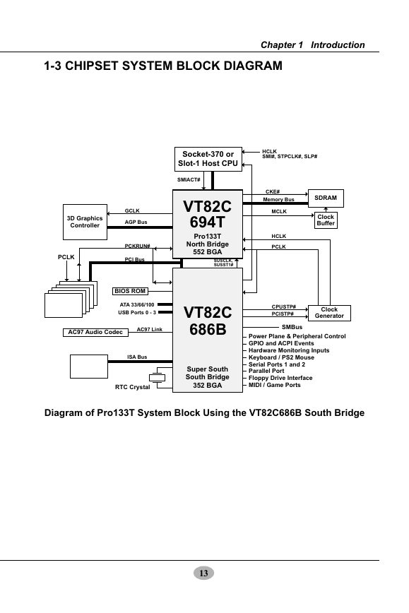
1-3 CHIPSET SYSTEM BLOCK DIAGRAM
Chapter 1 Introduction
Socket-370 or
Slot-1 Host CPU
SMIACT#
VT82C
694T
Pro133T
North Bridge
552 BGA
SUSCLK,
SUSST1#
HCLK
SMI#, STPCLK#, SLP#
CKE#
Memory Bus
MCLK
HCLK
PCLK
SDRAM
Clock
Buffer
VT82C
686B Power Plane & Peripheral Control
CPUSTP#
PCISTP#
SMBus
Clock
Generator
3D Graphics
Controller
PCLK
GCLK
AGP Bus
PCKRUN#
PCI Bus
BIOS ROM
ATA 33/66/100
USB Ports 0 - 3
AC97 Audio Codec
AC97 Link
ISA Bus
RTC Crystal
Super South
South Bridge
352 BGA
GPIO and ACPI Events
Hardware Monitoring Inputs
Keyboard / PS2 Mouse
Serial Ports 1 and 2
Parallel Port
Floppy Drive Interface
MIDI / Game Ports
Diagram of Pro133T System Block Using the VT82C686B South Bridge
13
�
65KV2-CT
MEMOMEMO
14
�


 2023年江西萍乡中考道德与法治真题及答案.doc
 2012年重庆南川中考生物真题及答案.doc
 2013年江西师范大学地理学综合及文艺理论基础考研真题.doc
 2020年四川甘孜小升初语文真题及答案I卷.doc
 2020年注册岩土工程师专业基础考试真题及答案.doc
 2023-2024学年福建省厦门市九年级上学期数学月考试题及答案.doc
 2021-2022学年辽宁省沈阳市大东区九年级上学期语文期末试题及答案.doc
 2022-2023学年北京东城区初三第一学期物理期末试卷及答案.doc
 2018上半年江西教师资格初中地理学科知识与教学能力真题及答案.doc
 2012年河北国家公务员申论考试真题及答案-省级.doc
 2020-2021学年江苏省扬州市江都区邵樊片九年级上学期数学第一次质量检测试题及答案.doc
 2022下半年黑龙江教师资格证中学综合素质真题及答案.doc