ETA1188
10A Input, 9V/3A or 12V/2A Output BOOST Converter with True-Shutoff
DESCRIPTION
ETA1188 is a high power, high-efficiency, synchronous
boost that can output up to 27W of power. With
integrated high power MOSEFTs, it comfortably delivers
9V/3A output from a wide range of input voltage. It also
integrates an output short protection MOSEFT on chip to
provide over current protection and true-shutoff function.
With its tiny package of QFN3x3-20, it sports a small
footprint which makes it an ideal all-in-one solution for
high power boost applications.
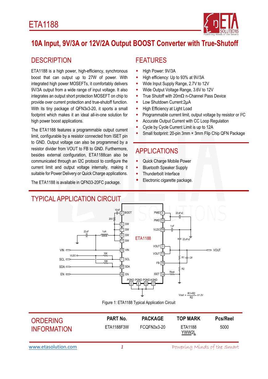
The ETA1188 features a programmable output current
limit, configurable by a resistor connected from ISET pin
to GND. Output voltage can also be programmed by a
resistor divider from VOUT to FB to GND. Furthermore,
besides external configuration, ETA1188can also be
communicated through an I2C protocol to configure the
current limit and output voltage internally, making it
suitable for Power Delivery or Quick Charge applications.
The ETA1188 is available in QFN33-20FC package.
TYPICAL APPLICATION CIRCUIT
FEATURES
High Power: 9V/3A
High efficiency: Up to 93% at 9V/3A
Wide Input Supply Range, 2.7V to 12V
Wide Output Voltage Range, 3.6V to 12V
True Shutoff with 20mΩ n-Channel Pass Device
Low Shutdown Current:2µA
High Efficiency at Light Load
Programmable current limit, output voltage by resistor or I2C
Accurate Output Current with CC Loop Regulation
Cycle by Cycle Current Limit is up to 12A
Small footprint: 20-pin 3mm × 3mm Flip Chip QFN Package
APPLICATIONS
Quick Charge Mobile Power
Bluetooth Speaker Supply
Thunderbolt Interface
Electronic cigarette package.
22uFx2
1uF
10nF
2
BOOT
200
5
7
9
11
SW
SW
SW
SW
15
VIN
1
SCL
20
SDA
22uF
1uH
10K
10K
ETA1188
PMID
4
PMID
12
VLDO
19
VOUT
3
VOUT
13
FB
16
22uFx2
R1
Cff
R2
VOUT
18
EN
PGND PGND PGND AGND
ISET
6
8
10
17
Riset
14
Figure 1: ETA1188 Typical Application Circuit
Vout =
R1+R2
R2
X1.2V
PART No.
ETA1188F3W
PACKAGE
FCQFN3x3-20
TOP MARK
ETA1188
YWW2L
Pcs/Reel
5000
1
Powering Minds of the Smart
VLDO
VIN
SCL
SDA
EN
ORDERING
INFORMATION
www.etasolution.com
�
ETA1188
PIN CONFIGURATION
A
D
S
20
O
D
L
V
19
N
E
18
D
N
G
A
17
B
F
16
SCL
BOOT
VOUT
PMID
SW
1
2
3
4
5
ETA1188
VOUT
PMID
SW
SW
6
7
8
9
W
S
D
N
G
P
D
N
G
P
W
S
10
D
N
G
P
FCQFN3x3 - 20
15
14
13
12
11
VIN
ISET
VOUT
PMID
SW
ELECTRICAL CHARACTERISTICS
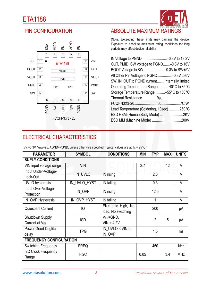
ABSOLUTE MAXIMUM RATINGS
(Note: Exceeding these limits may damage the device.
Exposure to absolute maximum rating conditions for long
periods may affect device reliability.)
IN Voltage to PGND..........................–0.3V to 13.2V
OUT, PMID, SW Voltage to PGND.......–0.3V to 16V
BOOT Voltage to SW......................–0.3V to SW+5V
All Other Pin Voltage to PGND...............–0.3V to 6V
SW, IN, OUT to PGND current........Internally limited
Operating Temperature Range .........–40°C to 85°C
Storage Temperature Range ..........–55°C to 150°C
Thermal Resistance θJA
FCQFN3X3-20........................30....................oC/W
Lead Temperature (Soldering, 10sec) ...........260°C
ESD HBM (Human Body Mode) ........................2KV
ESD MM (Machine Mode) ..............................200V
(VIN =3.3V, VOUT=9V, AGND=PGND, unless otherwise specified. Typical values are at TA = 25°C.)
MIN
PARAMETER
CONDITIONS
TYP MAX UNITS
IN rising
IN falling
IN rising
IN falling
EN=Logic High, No
load, No switching
VEN=GND,
VIN = 4.2V
IN_UVLO < VIN <
IN_OVP
2.7
0.05
2.6
0.3
12.5
1
200
2
1.5
450
12
5
V
V
V
V
V
μA
μA
ms
3.4
kHz
MHz
SYMBOL
VIN
IN_UVLO
IN_UVLO_HYST
IN_OVP
IN_OVP_HYST
SUPLY CONDITIONS
VIN input voltage range
Input Under-Voltage-
Lock-Out
UVLO hysteresis
Input Over-Voltage-
Protection
IN_OVP Hysteresis
Quiescent Current
Shutdown Supply
Current at VIN
Power Good Deglitch
delay
FREQUENCY CONFIGURATION
Switching Frequency
I2C Clock Frequency
Range
IQ
ISD
TPG
FREQ
FI2C
www.etasolution.com
2
Powering Minds of the Smart
�
ETA1188
OUTPUT CONFIGURATION
Feedback Voltage
FB Leakage Current
ISET Pin Voltage
ISET Output Current
ratio
Output Current Limit
VFB
IFB
VISET
KISET
VOUT_ILIM
0.98
VOUT =4.5V to 12.6V 1.176
VOUT ≥
VOUT_LOWV
VOUT <
VOUT_LOWV
KISET = IQ1 / IISET
Adjustable,
RISET=1.6kΩ
Adjustable,
RISET=1.6kΩ
0.78
1.2
0
1.0
0.8
1.224
1.02
0.82
5000
3.125
3
12
750
270
13.6
1
250
500
2.5
200
1.38
90
0.60
4.4
13.2
155
V
nA
V
V
A
A
A
mA
mA
V
mV
mV
V
mV
V
mV
V
ms
ms
°C
IPEAK
IMIN
IQZX
VOUT_IFB
PMID_OVP
Output Current Foldback
Switching Cycle-by-
Cycle Lowside current
limit
Minimum Inductor
Current each cycle
Inductor Zero Crossing
Current Stopping
threshold
PROTECTION
PMID Over Voltage
Protection
PMID_OVP Hysteresis
VOUT falling,
VOUT enter deep
VOUT- VIN
condition threshold
VOUT rising over
VOUT exits deep
VIN
condition threshold
Q1 Swapping sensing
VOUT rising
threshold
VOUT_HIGH Hysteresis VOUT_HIGH_HYST VOUT falling
FB Over-Voltage-
Protection
VFB_OVP Hystersis
Output Under Voltage
Protection
Hiccup Retrying Timer
Hiccup Disable Timer
Thermal Shutdown
To stop switching
Track FB pin
Voltage
Regulator enabled
Regulator disabled
Rising,
Hysteresis=20°C
PMID_OVP_HYST
VDEEP_ENTER
FB_UVP
THCON
THCOFF
VFB_OVP_HYST
VDEEP_EXIT
VOUT_HIGH
VFB_OVP
TSD
www.etasolution.com
3
Powering Minds of the Smart
�
2Meg resistor from
EN to GND, VEN =
1V.
1.2
VOUT = 9V,
VFB=1.5V,VSW=0 or
9V, VEN=GND
SLEW[1:0] = 00
SLEW[1:0] = 01
SLEW[1:0] = 10
SLEW[1:0] = 11
VOREG_INT[ ] = 1
3.6
1
20
18
14
0.4
μA
V
V
mΩ
mΩ
mΩ
10
μA
18
9
4.5
2.25
12
mV/μs
V
4000
mA
VOUT_INT
ILIM_INT
IOREG_INT[ ] = 1
500
ETA1188
LOGIC PINS, EN, SDA, SCL
Input Current
logic high voltage
logic low voltage
POWER FETS
PMID to OUT Switch On
Resistance
Highside Switch On
Resistance
Lowside Switch On
Resistance
RQ1
RQ2
RQ3
SW Leakage Current
SW_LKG
INTERNAL VOUT SETTING
VOUT ramping slew rate
VOUT_SLEW
Internal VOUT setting
range
Internal VOUT current
limit range
www.etasolution.com
4
Powering Minds of the Smart
�
ETA1188
PIN DESCRIPTION
PIN #
PIN NAME
DESCRIPTION
1
2
3, 13
4, 12
5, 7, 9, 11
6, 8, 10
14
15
16
17
18
19
20
SCL
BOOT
VOUT
PMID
SW
PGND
ISET
VIN
FB
AGND
EN
VLDO
SDA
I2C interface clock. Connect a 10-kΩ pull up resistor to VLDO or external 3.3V
rail.
Bootstrap capacitor connection for the high-side FET gate driver. Connect a
10-nF ceramic capacitor (voltage rating ≥ 10 V) from BOOT pin to SW pin.
Output pins. Connect a 2x22uF to GND
Midpoint of the Boost output and current limit switch. Connect a 22uF to GND
Switching Pin. Connect with an inductor between this pin and input.
Power Ground.
Boost maximum output current setting. Connect a resistor between this pin
and analog ground to set the current level.
Input pin. Connect to Battery or input supply. Bypass with a 22uF capacitor
from this pin to ground.
Feedback pin for setting up the boost output voltage.
Analog Ground pin.
Enable pin for the IC.
LDO Regulator Output. Bypass with 1uF capacitor from this pin to ground.
I2C interface data. Connect a 10-kΩ pull up resistor to VLDO or external 3.3V
rail.
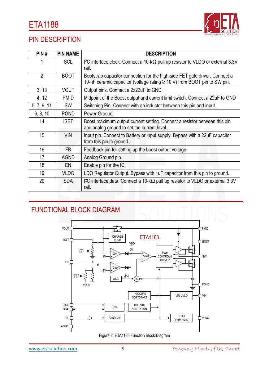
FUNCTIONAL BLOCK DIAGRAM
VOUT
ISET
FB
SCL
SDA
EN
AGND
CHARGE
PUMP
VDD
ETA1188
PWM
CONTROL&
DRIVER
IOREG
[2:0]
VOREG
[8:0]
VOUT
1V
1.2V
Gmi
Gmv
OSC
I2C
BANDGAP
COMP
Σ
HICCUP &
SOFTSTART
THERMAL
SHUTDOWN
Figure 2: ETA1188 Function Block Diagram
PMID
BOOT
SW
PGND
VIN
VIN UVLO
LDO
( From PMID)
VLDO
www.etasolution.com
5
Powering Minds of the Smart
�
ETA1188
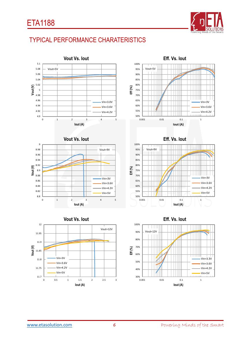
TYPICAL PERFORMANCE CHARATERISTICS
Vout Vs. Iout
Vout=5V
Eff. Vs. Iout
Vout=5V
100%
95%
90%
85%
80%
75%
70%
65%
60%
55%
)
%
(
f
f
E
Vin=3.0V
Vin=3.6V
Vin=4.2V
0
1
2
3
4
5
50%
0.001
0.01
Iout (A)
Vout Vs. Iout
Vout=9V
Vin=3V
Vin=3.6V
Vin=4.2V
Vin=5V
0
1
2
3
4
5
Iout (A)
Vout Vs. Iout
Vout=12V
Vin=3V
Vin=3.6V
Vin=4.2V
Vin=5V
0.1
Iout (A)
Eff. Vs. Iout
Vout=9V
100%
95%
90%
85%
80%
75%
70%
65%
60%
55%
)
%
(
f
f
E
50%
0.001
0.01
0.1
Iout (A)
Eff. Vs. Iout
Vout=12V
100%
90%
80%
70%
60%
50%
40%
)
%
(
f
f
E
30%
0.001
0.01
0.1
Iout (A)
)
V
(
t
u
o
V
)
V
(
t
u
o
V
5.1
5.08
5.06
5.04
5.02
5
4.98
4.96
4.94
4.92
4.9
9
8.98
8.96
8.94
8.92
8.9
8.88
8.86
8.84
8.82
8.8
12
11.95
11.9
11.85
11.8
11.75
)
V
(
t
u
o
V
Vin=3V
Vin=3.6V
Vin=4.2V
1
Vin=3V
Vin=3.6V
Vin=4.2V
Vin=5V
1
Vin=3.3V
Vin=3.6V
Vin=4.2V
Vin=5V
1
11.7
0
0.5
1
2
2.5
3
1.5
Iout (A)
www.etasolution.com
6
Powering Minds of the Smart
�
ETA1188
TYPICAL PERFORMANCE CHARATERISTICS (cont’)
Load Transient, VOUT = 5V, 1A – 2A, VIN = 4.2V
500us/div
Iout Limit Vs. Riset
)
A
(
t
i
m
i
l
I
5
4.5
4
3.5
3
2.5
2
1.5
1
0.5
0
0
2
4
6
Riset (Kohm)
8
10
200mV/div
VOUT
IOUT
1A/div
200mV/div
VOUT
IOUT
1A/div
200mV/div
VOUT
IOUT
1A/div
Load Transient, VOUT = 9V, 1A – 2A, VIN = 4.2V
Load Transient, VOUT = 12V, 1A – 2A, VIN = 4.2V
500us/div
500us/div
Switching in DCM, VOUT = 5V,
IOUT = 100mA, VIN = 4.2V
5us/div
Switching in CCM, VOUT = 5V,
IOUT = 2A, VIN = 4.2V
1us/div
SW
5V/div
VOUT
20mV/div
ILX
2A/div
www.etasolution.com
50mV/div
VOUT
SW
5V/div
ILX
2A/div
7
Powering Minds of the Smart
�
ETA1188
TYPICAL PERFORMANCE CHARATERISTICS (cont’)
Switching in DCM, VOUT = 9V,
IOUT = 100mA, VIN = 4.2V
1us/div
Switching in CCM, VOUT = 9V,
IOUT = 2A, VIN = 4.2V
1us/div
100mV/div
VOUT
SW
5V/div
ILX
2A/div
Switching in DCM, VOUT = 12V,
IOUT = 100mA, VIN = 4.2V
Switching in CCM, VOUT = 12V,
IOUT = 100mA, VIN = 4.2V
2us/div
VOUT
2us/div
50mV/div
VOUT
SW
5V/div
ILX
2A/div
VOUT
20mV/div
SW
5V/div
ILX
2A/div
Start-up no load, VOUT = 5V, VIN = 4.2V
500us/div
5V/div
EN
PMID
2V/div
2V/div
VOUT
ILX
5A/div
20mV/div
SW
10V/div
ILX
2A/div
Start-up, ROUT = 3Ω, VOUT = 5V, VIN = 4.2V
500us/div
5V/div
EN
PMID
2V/div
2V/div
VOUT
ILX
5A/div
www.etasolution.com
8
Powering Minds of the Smart
�


 V2版本原理图(Capacitive-Fingerprint-Reader-Schematic_V2).pdf
 摄像头工作原理.doc
 VL53L0X简要说明(En.FLVL53L00216).pdf
 原理图(DVK720-Schematic).pdf
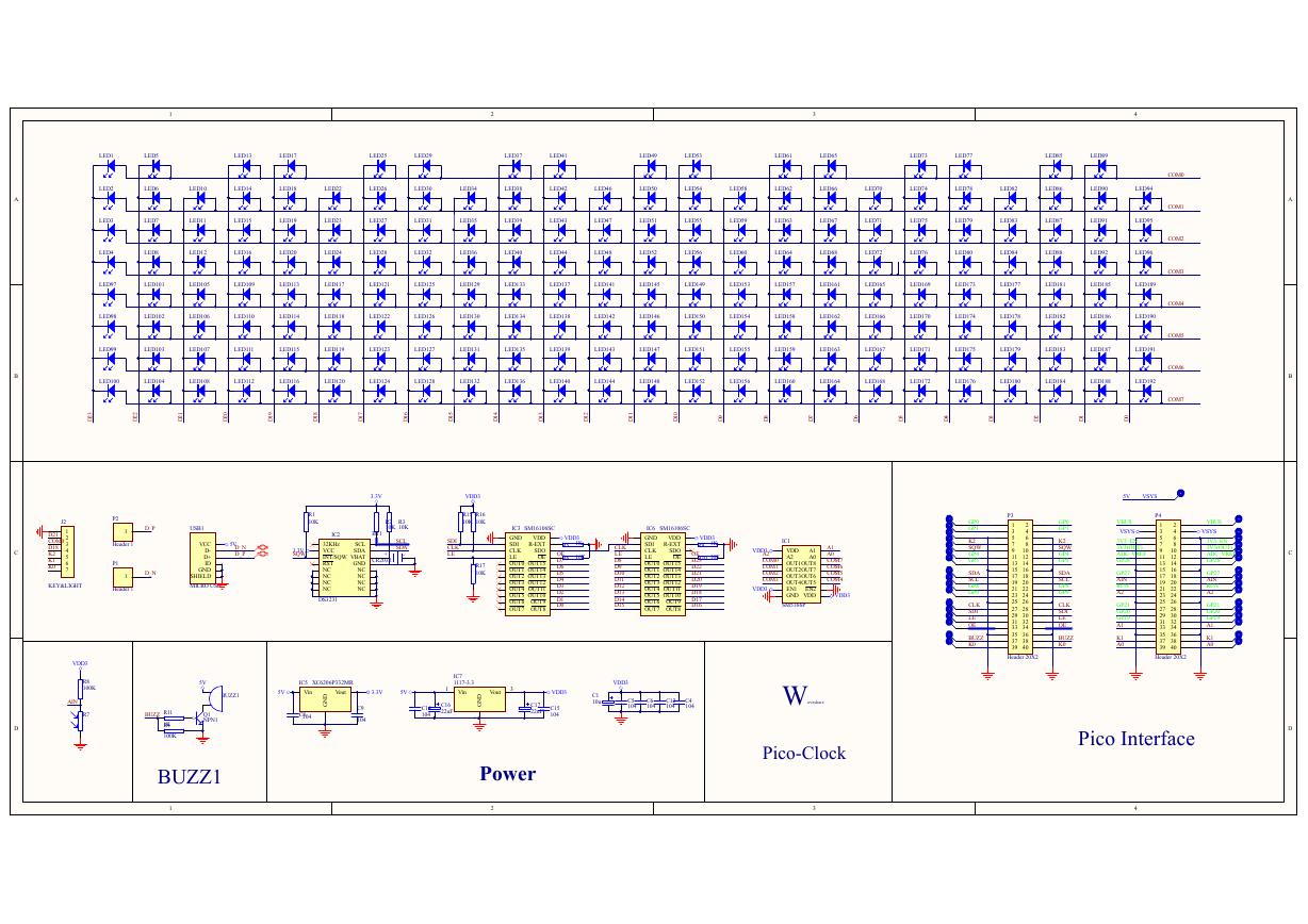 原理图(Pico-Clock-Green-Schdoc).pdf
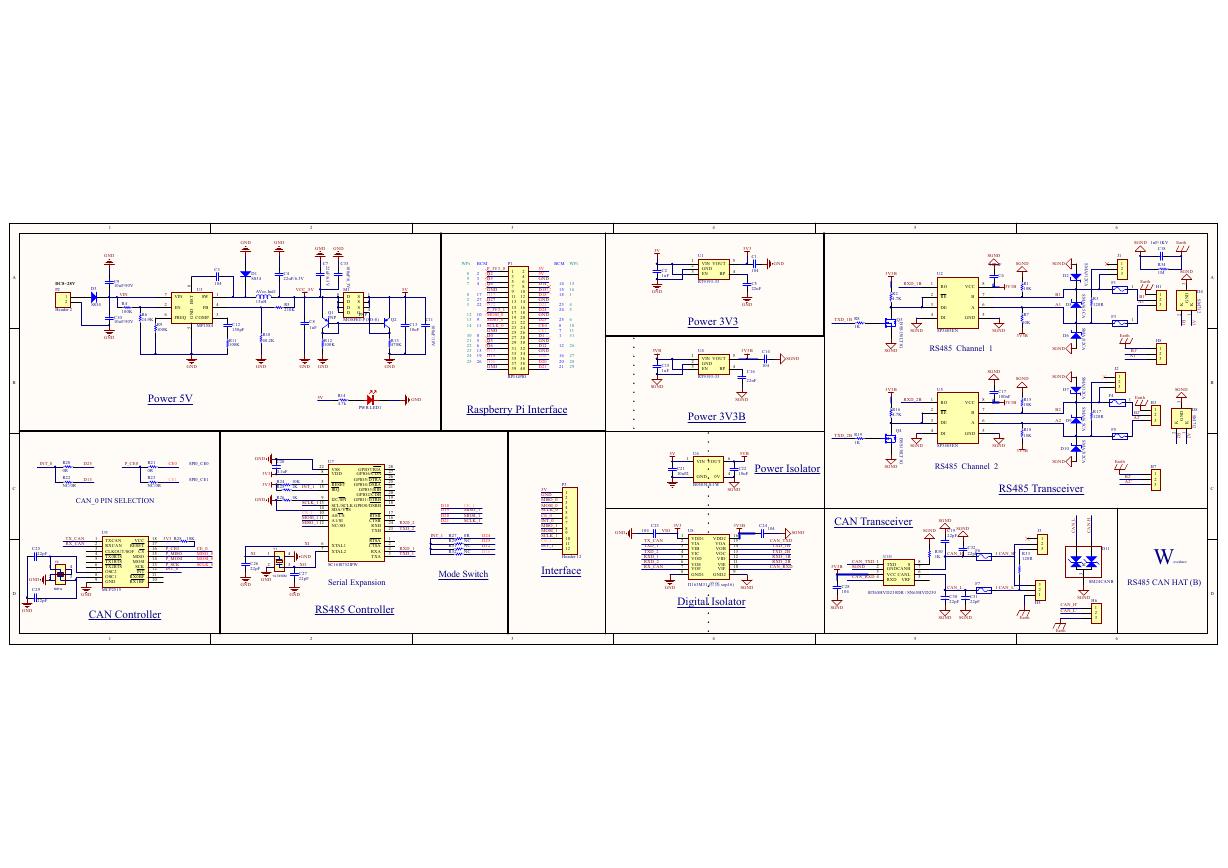 原理图(RS485-CAN-HAT-B-schematic).pdf
 File:SIM7500_SIM7600_SIM7800 Series_SSL_Application Note_V2.00.pdf
 ADS1263(Ads1262).pdf
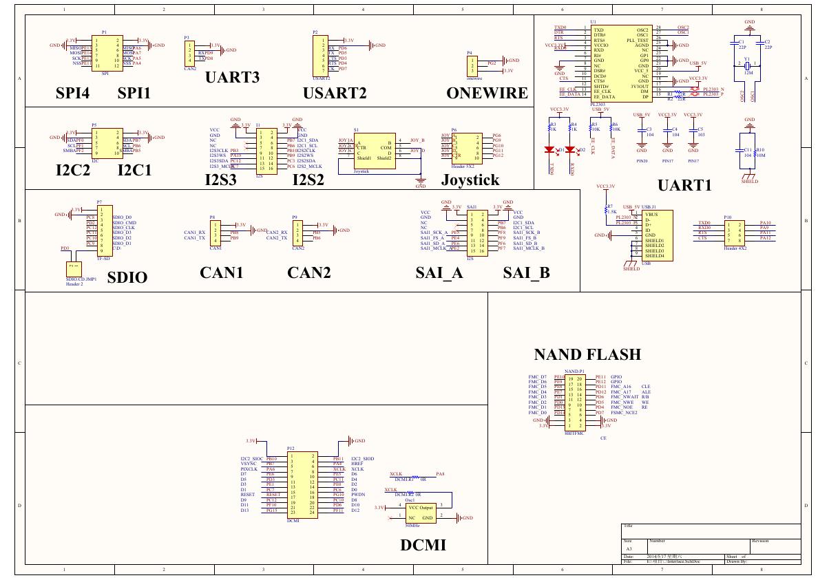 原理图(Open429Z-D-Schematic).pdf
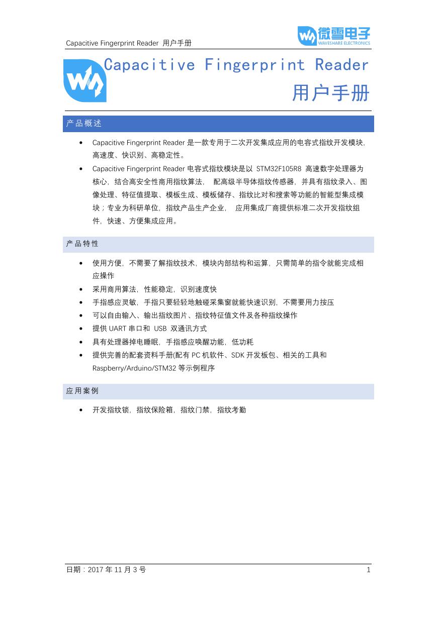 用户手册(Capacitive_Fingerprint_Reader_User_Manual_CN).pdf
 CY7C68013A(英文版)(CY7C68013A).pdf
 TechnicalReference_Dem.pdf