FT232RN USB UART IC Datasheet
Version 1.1
Document No.: FT_001521 Clearance No.: FTDI#571
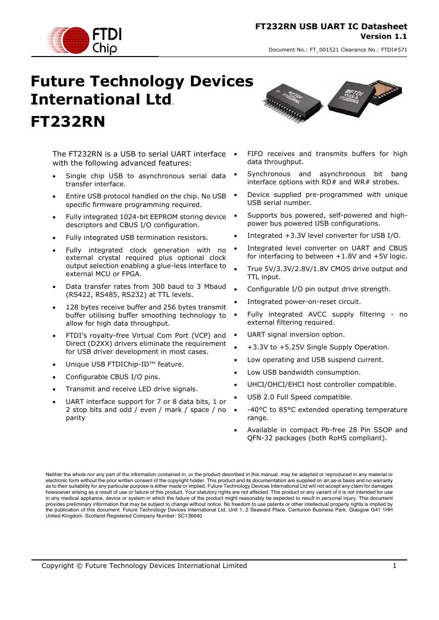
Future Technology Devices
International Ltd.
FT232RN
The FT232RN is a USB to serial UART interface
with the following advanced features:
•
FIFO receives and transmits buffers for high
data throughput.
• Single chip USB to asynchronous serial data
transfer interface.
• Synchronous and asynchronous bit bang
interface options with RD# and WR# strobes.
•
•
•
•
Entire USB protocol handled on the chip. No USB
specific firmware programming required.
• Device supplied pre-programmed with unique
USB serial number.
Fully integrated 1024-bit EEPROM storing device
descriptors and CBUS I/O configuration.
• Supports bus powered, self-powered and high-
power bus powered USB configurations.
Fully integrated USB termination resistors.
Fully
integrated clock generation with no
external crystal required plus optional clock
output selection enabling a glue-less interface to
external MCU or FPGA.
•
•
•
Integrated +3.3V level converter for USB I/O.
Integrated level converter on UART and CBUS
for interfacing to between +1.8V and +5V logic.
True 5V/3.3V/2.8V/1.8V CMOS drive output and
TTL input.
• Data transfer rates from 300 baud to 3 Mbaud
(RS422, RS485, RS232) at TTL levels.
• 128 bytes receive buffer and 256 bytes transmit
buffer utilising buffer smoothing technology to
allow for high data throughput.
•
FTDI’s royalty-free Virtual Com Port (VCP) and
Direct (D2XX) drivers eliminate the requirement
for USB driver development in most cases.
• Unique USB FTDIChip-ID™ feature.
• Configurable CBUS I/O pins.
•
Transmit and receive LED drive signals.
• UART interface support for 7 or 8 data bits, 1 or
2 stop bits and odd / even / mark / space / no
parity
• Configurable I/O pin output drive strength.
•
•
Integrated power-on-reset circuit.
Fully integrated AVCC supply filtering - no
external filtering required.
• UART signal inversion option.
• +3.3V to +5.25V Single Supply Operation.
•
•
Low operating and USB suspend current.
Low USB bandwidth consumption.
• UHCI/OHCI/EHCI host controller compatible.
• USB 2.0 Full Speed compatible.
•
-40°C to 85°C extended operating temperature
range.
• Available in compact Pb-free 28 Pin SSOP and
QFN-32 packages (both RoHS compliant).
Neither the whole nor any part of the information contained in, or the product described in this manual, may be adapted or reproduced in any material or
electronic form without the prior written consent of the copyright holder. This product and its documentation are supplied on an as-is basis and no warranty
as to their suitability for any particular purpose is either made or implied. Future Technology Devices International Ltd will not accept any claim for damages
howsoever arising as a result of use or failure of this product. Your statutory rights are not affected. This product or any variant of it is not intended for use
in any medical appliance, device or system in which the failure of the product might reasonably be expected to result in personal injury. This document
provides preliminary information that may be subject to change without notice. No freedom to use patents or other intellectual property rights is implied by
the publication of this document. Future Technology Devices International Ltd, Unit 1, 2 Seaward Place, Centurion Business Park, Glasgow G41 1HH
United Kingdom. Scotland Registered Company Number: SC136640
Copyright © Future Technology Devices International Limited
1
�
1
Typical Applications
FT232RN USB UART IC Datasheet
Version 1.1
Document No.: FT_001521 Clearance No.: FTDI#571
• USB to RS232/RS422/RS485 Converters
• USB Industrial Control
• Upgrading Legacy Peripherals to USB
• USB MP3 Player Interface
• Cellular and Cordless Phone USB data transfer
• USB FLASH Card Reader and Writers
cables and interfaces
•
Interfacing MCU/PLD/FPGA based designs to
USB
• USB Audio and Low Bandwidth Video data
transfer
•
PDA to USB data transfer
• USB Smart Card Readers
• USB Instrumentation
1.1 Driver Support
• Set Top Box PC - USB interface
• USB Digital Camera Interface
• USB Hardware Modems
• USB Wireless Modems
• USB Bar Code Readers
• USB Software and Hardware Encryption
Dongles
Royalty free VIRTUAL COM PORT
(VCP) DRIVERS for...
Royalty free D2XX Direct Drivers
(USB Drivers + DLL S/W Interface)
• Windows 11,64-bit
• Windows 11,64-bit
• Windows 10 32,64-bit
• Windows 10 32,64-bit
• Windows 8/8.1 32,64-bit
• Windows 8/8.1 32,64-bit
• Windows 7 32,64-bit
• Windows 7 32,64-bit
• Windows Server 2008 and Server 2012 R2
• Server 2008 and Server 2012 R2
• Mac OS
• Mac OS
•
Linux 2.4 and greater
•
Linux 2.4 and greater
• Android(J2xx)
The drivers listed above are all available to download for free from FTDI website (www.ftdichip.com).
Various 3rd party drivers are also available for other operating systems - see FTDI website
(www.ftdichip.com) for details.
For driver installation, please refer to http://www.ftdichip.com/Documents/InstallGuides.htm
1.2 Part Numbers
Part Number
FT232RNQ-xxxx
FT232RNL-xxxx
Package
32 Pin QFN
28 Pin SSOP
Note: Packing codes for xxxx is:
- Reel: Taped and Reel, (SSOP is 2,000pcs per reel, QFN is 6,000pcs per reel).
- Tube: Tube packing, 47pcs per tube (SSOP only)
- Tray: Tray packing, 490pcs per tray (QFN only)
For example: FT232RNQ-Reel is 6,000pcs taped and reel packing
Copyright © Future Technology Devices International Limited
2
�
FT232RN USB UART IC Datasheet
Version 1.1
Document No.: FT_001521 Clearance No.: FTDI#571
1.3 USB Compliant
The FT232RN is fully compliant with the USB 2.0 specification and has been given the USB-IF Test-ID (TID)
6654.
Copyright © Future Technology Devices International Limited
3
�
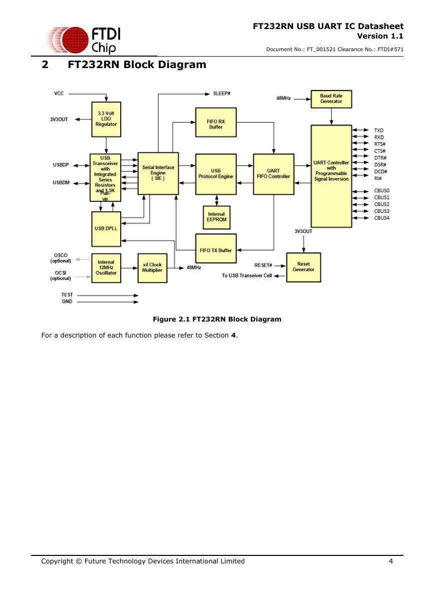
FT232RN Block Diagram
2
FT232RN USB UART IC Datasheet
Version 1.1
Document No.: FT_001521 Clearance No.: FTDI#571
For a description of each function please refer to Section 4.
Figure 2.1 FT232RN Block Diagram
Copyright © Future Technology Devices International Limited
4
�
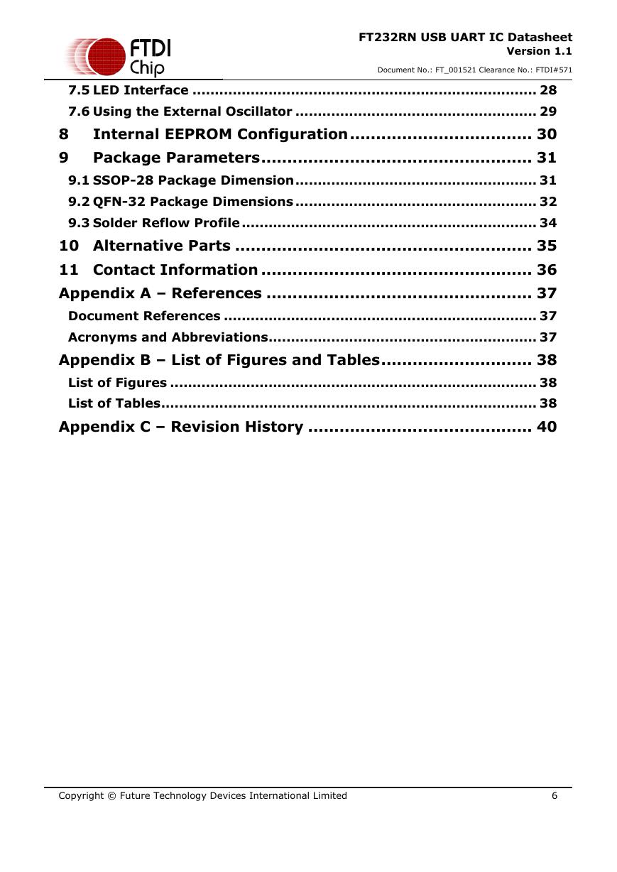
Table of Contents
FT232RN USB UART IC Datasheet
Version 1.1
Document No.: FT_001521 Clearance No.: FTDI#571
1
Typical Applications ....................................................... 2
1.1 Driver Support .............................................................................. 2
1.2 Part Numbers ............................................................................... 2
1.3 USB Compliant .............................................................................. 3
2
FT232RN Block Diagram ................................................ 4
3 Device Pin Out and Signal Description ........................... 7
3.1 28-LD SSOP Package .................................................................... 7
3.2 SSOP Package Pin Out Description ............................................... 7
3.3 QFN-32 Package ........................................................................... 9
3.4 QFN-32 Package Signal Description .............................................. 9
3.5 CBUS Signal Options ................................................................... 11
4
Function Description ................................................... 12
4.1 Key Features .............................................................................. 12
4.2 Functional Block Descriptions ..................................................... 13
5 Devices Characteristics and Ratings ............................ 15
5.1 Absolute Maximum Ratings ........................................................ 15
5.2 DC Characteristics ...................................................................... 15
5.3 EEPROM Reliability Characteristics ............................................. 17
5.4 Internal Clock Characteristics .................................................... 17
5.5 Thermal Characteristics .............................................................. 18
6 USB Power Configurations ........................................... 19
6.1 USB Bus Powered Configuration ................................................ 19
6.2 Self Powered Configuration ........................................................ 20
6.3 USB Bus Powered with Power Switching Configuration .............. 21
6.4 USB Bus Powered with Selectable External Logic Supply ........... 22
7 Application Examples .................................................. 24
7.1 USB to RS232 Converter ............................................................. 24
7.2 USB to RS485 Converter ............................................................. 25
7.3 USB to RS422 Converter ............................................................. 26
7.4 USB to MCU UART Interface ........................................................ 27
Copyright © Future Technology Devices International Limited
5
�
FT232RN USB UART IC Datasheet
Version 1.1
Document No.: FT_001521 Clearance No.: FTDI#571
7.5 LED Interface ............................................................................. 28
7.6 Using the External Oscillator ...................................................... 29
8
Internal EEPROM Configuration ................................... 30
9 Package Parameters .................................................... 31
9.1 SSOP-28 Package Dimension ...................................................... 31
9.2 QFN-32 Package Dimensions ...................................................... 32
9.3 Solder Reflow Profile .................................................................. 34
10 Alternative Parts ......................................................... 35
11 Contact Information .................................................... 36
Appendix A – References ................................................... 37
Document References ...................................................................... 37
Acronyms and Abbreviations ............................................................ 37
Appendix B – List of Figures and Tables ............................. 38
List of Figures .................................................................................. 38
List of Tables .................................................................................... 38
Appendix C – Revision History ........................................... 40
Copyright © Future Technology Devices International Limited
6
�
FT232RN USB UART IC Datasheet
Version 1.1
Document No.: FT_001521 Clearance No.: FTDI#571
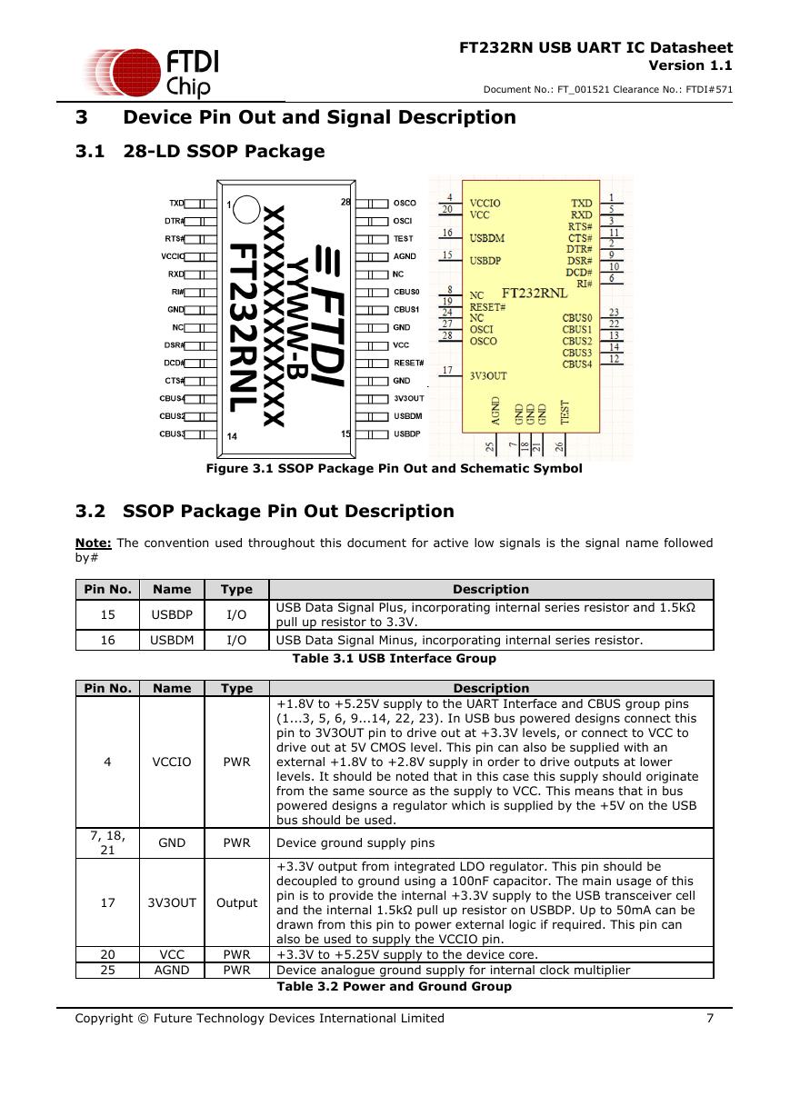
3 Device Pin Out and Signal Description
3.1 28-LD SSOP Package
Figure 3.1 SSOP Package Pin Out and Schematic Symbol
3.2 SSOP Package Pin Out Description
Note: The convention used throughout this document for active low signals is the signal name followed
by#
Pin No. Name
Type
Description
15
16
USBDP
I/O
USB Data Signal Plus, incorporating internal series resistor and 1.5kΩ
pull up resistor to 3.3V.
USBDM
I/O
USB Data Signal Minus, incorporating internal series resistor.
Table 3.1 USB Interface Group
Pin No. Name
Type
Description
4
VCCIO
PWR
+1.8V to +5.25V supply to the UART Interface and CBUS group pins
(1...3, 5, 6, 9...14, 22, 23). In USB bus powered designs connect this
pin to 3V3OUT pin to drive out at +3.3V levels, or connect to VCC to
drive out at 5V CMOS level. This pin can also be supplied with an
external +1.8V to +2.8V supply in order to drive outputs at lower
levels. It should be noted that in this case this supply should originate
from the same source as the supply to VCC. This means that in bus
powered designs a regulator which is supplied by the +5V on the USB
bus should be used.
7, 18,
21
GND
PWR
Device ground supply pins
17
3V3OUT Output
20
25
VCC
AGND
PWR
PWR
+3.3V output from integrated LDO regulator. This pin should be
decoupled to ground using a 100nF capacitor. The main usage of this
pin is to provide the internal +3.3V supply to the USB transceiver cell
and the internal 1.5kΩ pull up resistor on USBDP. Up to 50mA can be
drawn from this pin to power external logic if required. This pin can
also be used to supply the VCCIO pin.
+3.3V to +5.25V supply to the device core.
Device analogue ground supply for internal clock multiplier
Table 3.2 Power and Ground Group
Copyright © Future Technology Devices International Limited
7
�
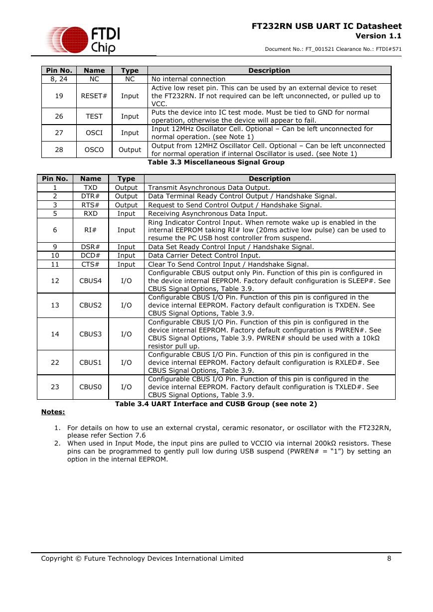
Pin No. Name
Type
8, 24
NC
NC
19
RESET#
Input
26
27
28
TEST
Input
OSCI
Input
OSCO
Output
FT232RN USB UART IC Datasheet
Version 1.1
Document No.: FT_001521 Clearance No.: FTDI#571
Description
No internal connection
Active low reset pin. This can be used by an external device to reset
the FT232RN. If not required can be left unconnected, or pulled up to
VCC.
Puts the device into IC test mode. Must be tied to GND for normal
operation, otherwise the device will appear to fail.
Input 12MHz Oscillator Cell. Optional – Can be left unconnected for
normal operation. (see Note 1)
Output from 12MHZ Oscillator Cell. Optional – Can be left unconnected
for normal operation if internal Oscillator is used. (see Note 1)
Table 3.3 Miscellaneous Signal Group
Pin No. Name
TXD
DTR#
RTS#
RXD
1
2
3
5
6
9
10
11
12
RI#
Input
DSR#
DCD#
CTS#
Input
Input
Input
CBUS4
I/O
13
CBUS2
I/O
14
CBUS3
I/O
22
CBUS1
I/O
23
CBUS0
I/O
Transmit Asynchronous Data Output.
Type
Output
Output Data Terminal Ready Control Output / Handshake Signal.
Output Request to Send Control Output / Handshake Signal.
Input
Description
Receiving Asynchronous Data Input.
Ring Indicator Control Input. When remote wake up is enabled in the
internal EEPROM taking RI# low (20ms active low pulse) can be used to
resume the PC USB host controller from suspend.
Data Set Ready Control Input / Handshake Signal.
Data Carrier Detect Control Input.
Clear To Send Control Input / Handshake Signal.
Configurable CBUS output only Pin. Function of this pin is configured in
the device internal EEPROM. Factory default configuration is SLEEP#. See
CBUS Signal Options, Table 3.9.
Configurable CBUS I/O Pin. Function of this pin is configured in the
device internal EEPROM. Factory default configuration is TXDEN. See
CBUS Signal Options, Table 3.9.
Configurable CBUS I/O Pin. Function of this pin is configured in the
device internal EEPROM. Factory default configuration is PWREN#. See
CBUS Signal Options, Table 3.9. PWREN# should be used with a 10kΩ
resistor pull up.
Configurable CBUS I/O Pin. Function of this pin is configured in the
device internal EEPROM. Factory default configuration is RXLED#. See
CBUS Signal Options, Table 3.9.
Configurable CBUS I/O Pin. Function of this pin is configured in the
device internal EEPROM. Factory default configuration is TXLED#. See
CBUS Signal Options, Table 3.9.
Notes:
Table 3.4 UART Interface and CUSB Group (see note 2)
1. For details on how to use an external crystal, ceramic resonator, or oscillator with the FT232RN,
please refer Section 7.6
2. When used in Input Mode, the input pins are pulled to VCCIO via internal 200kΩ resistors. These
pins can be programmed to gently pull low during USB suspend (PWREN# = “1”) by setting an
option in the internal EEPROM.
Copyright © Future Technology Devices International Limited
8
�



 V2版本原理图(Capacitive-Fingerprint-Reader-Schematic_V2).pdf
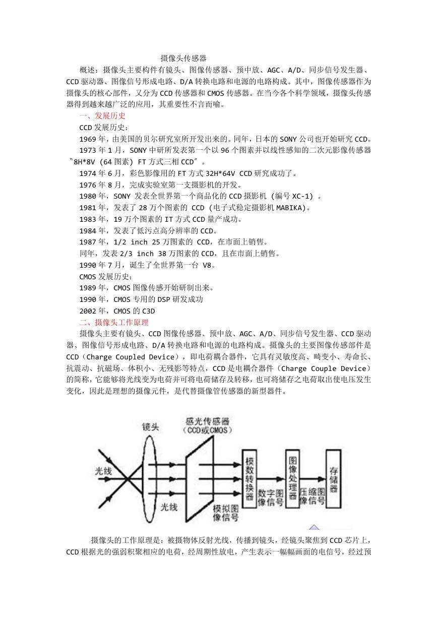 摄像头工作原理.doc
 VL53L0X简要说明(En.FLVL53L00216).pdf
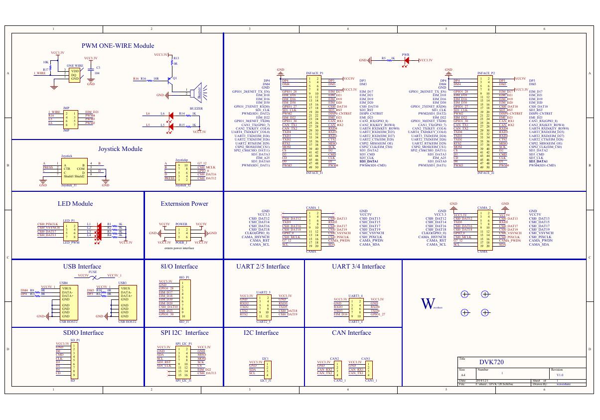 原理图(DVK720-Schematic).pdf
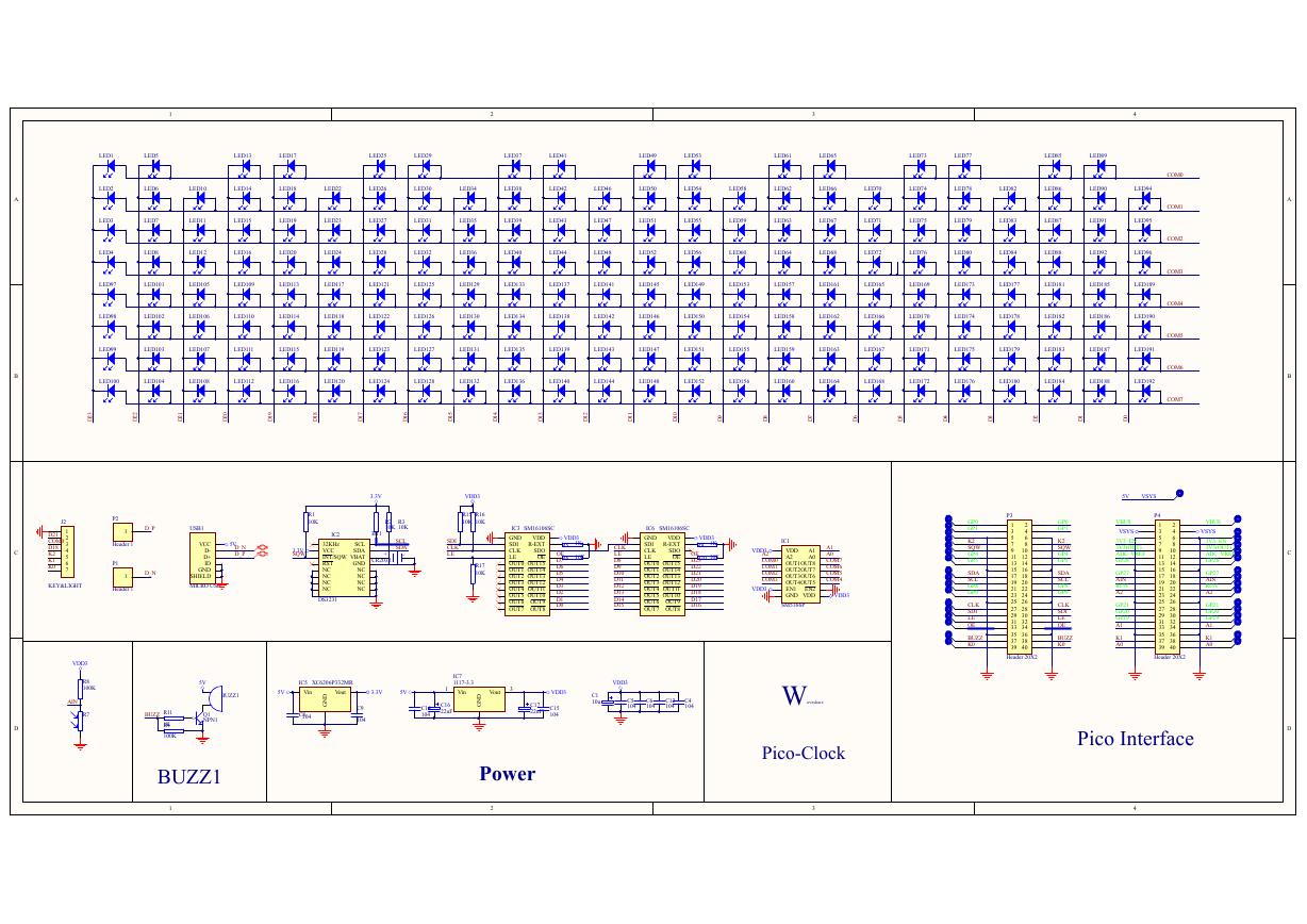 原理图(Pico-Clock-Green-Schdoc).pdf
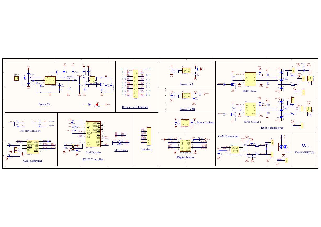 原理图(RS485-CAN-HAT-B-schematic).pdf
 File:SIM7500_SIM7600_SIM7800 Series_SSL_Application Note_V2.00.pdf
 ADS1263(Ads1262).pdf
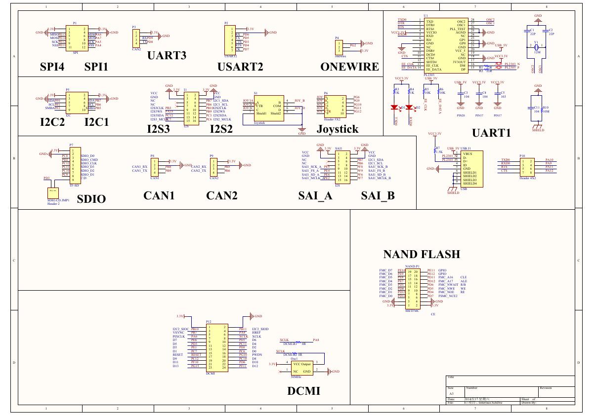 原理图(Open429Z-D-Schematic).pdf
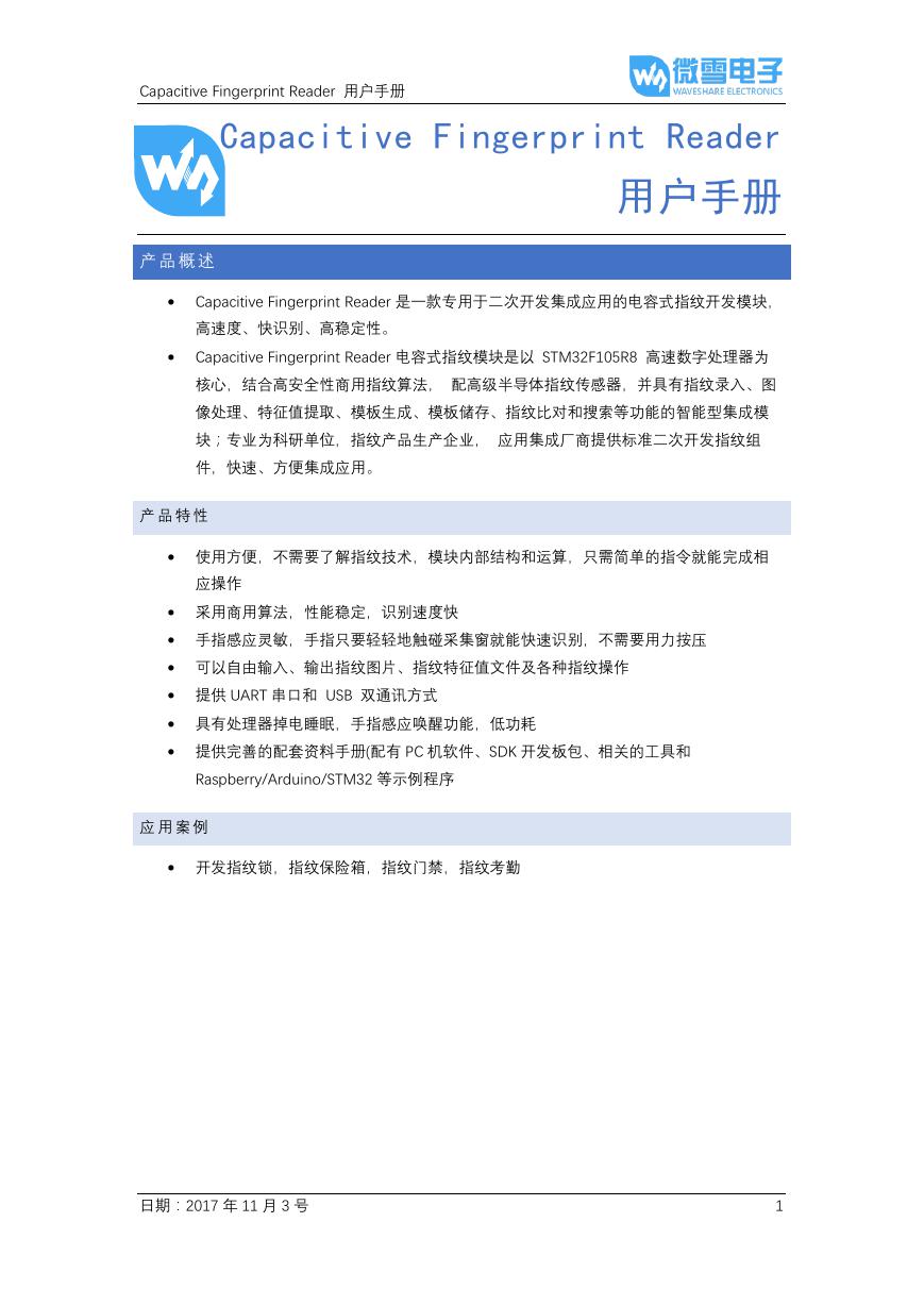 用户手册(Capacitive_Fingerprint_Reader_User_Manual_CN).pdf
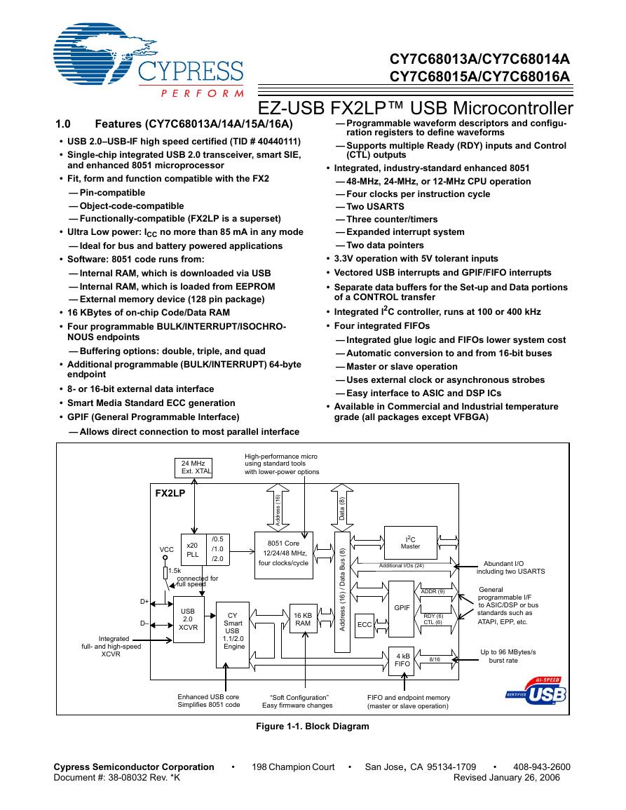 CY7C68013A(英文版)(CY7C68013A).pdf
 TechnicalReference_Dem.pdf