logo资料库

B27A_Fortis_Flash_512Gb_1Tb_2Tb_4Tb_Async_Sync_NAND_Datasheet.pd....pdf

第1页 / 共333页
第2页 / 共333页
第3页 / 共333页
第4页 / 共333页
第5页 / 共333页
第6页 / 共333页
第7页 / 共333页
第8页 / 共333页
资料共333页,剩余部分请下载后查看
NAND Flash Memory - FortisFlash™
B27A FortisFlash™ Features
Part Numbering Information
Important Notes and Warnings
General Description
Asynchronous, NV-DDR2, NV-DDR3 Signal Descriptions
Signal Assignments
Package Dimensions
Architecture
Device and Array Organization
Bus Operation – Asynchronous Interface
Asynchronous Enable/Standby
Asynchronous Bus Idle
Asynchronous Pausing Data Input/Output
Asynchronous Commands
Asynchronous Addresses
Asynchronous Data Input
Asynchronous Data Output
Write Protect
Ready/Busy#
Bus Operation – NV-DDR2 Interface
Differential Signaling
Warmup Cycles
On-die Termination (ODT)
Self-termination On-die Termination (ODT)
Matrix Termination
Matrix Termination Examples
NV-DDR2 Standby
NV-DDR2 Idle
NV-DDR2 Pausing Data Input/Output
NV-DDR2 Commands
NV-DDR2 Addresses
NV-DDR2 Data Input
NV-DDR2 Data Output
Write Protect
Ready/Busy#
Bus Operation – NV-DDR3 Interface
On-Die Termination
Device Initialization
VPP Initialization
Electronic Mirroring
Activating Interfaces
Activating the Asynchronous Interface
Activating the NV-DDR2 Interface
Activating the NV-DDR3 Interface
CE# Pin Reduction and Volume Addressing
Initialization Sequence
Volume Appointment Without CE# Pin Reduction
Appointing Volume Addresses
Selecting a Volume
Multiple Volume Operation Restrictions
Volume Reversion
Command Definitions
Reset Operations
RESET (FFh)
SYNCHRONOUS RESET (FCh)
RESET LUN (FAh)
HARD RESET (FDh)
Identification Operations
READ ID (90h)
READ ID Parameter Tables
READ PARAMETER PAGE (ECh)
Parameter Page Data Structure Tables
READ UNIQUE ID (EDh)
Configuration Operations
SET FEATURES (EFh)
GET/SET FEATURES by LUN (D4h/D5h)
Feature Address Details
SLC Operations
Configuration using SET FEATURES
Configuration using Commands (DAh, DFh)
SLC/TLC Mode Operations
VOLUME SELECT (E1h)
ODT CONFIGURE (E2h)
ZQ Calibration
ZQ Calibration Long (F9h)
ZQ Calibration Short (D9h)
ZQ external resistor value, tolerance, and capacitive loading
Status Operations
READ STATUS (70h)
READ STATUS ENHANCED (78h)
FIXED ADDRESS READ STATUS ENHANCED (71h)
Column Address Operations
CHANGE READ COLUMN (05h-E0h)
CHANGE READ COLUMN ENHANCED (06h-E0h)
CHANGE READ COLUMN ENHANCED (00h-05h-E0h) Operation
CHANGE WRITE COLUMN (85h)
CHANGE ROW ADDRESS (85h)
Read Operations
READ MODE (00h)
READ PAGE (00h-30h)
READ PAGE CACHE SEQUENTIAL (31h)
READ PAGE CACHE RANDOM (00h-31h)
READ PAGE CACHE LAST (3Fh)
READ PAGE MULTI-PLANE (00h-32h)
Read Retry Operations
Read Retry Scratch Space
SNAP READ
Snap Read Feature
SNAP READ MULTI-PLANE (00h-32h) - CROSS PLANE SNAP READ
READ OFFSET Operations
Auto Read Calibration Operations
Auto Read Calibration
Auto Read Calibration and Read Offset
Reading Out Calibrated Offsets With GET FEATURES (EEh/D4h)
Soft Data Read Operations
READ PAGE with SOFT INFORMATION (33h-30h)
SOFT INFORMATION READOUT (36h)
SOFT INFORMATION READOUT (36h) with the Level Indicator Bit
Single Bit Soft Bit Read Operations
SINGLE BIT SOFT BIT READ PAGE (00h-34h)
SINGLE BIT SOFT BIT READ PAGE CACHE RANDOM (00h-38h)
Word Line Status Bypass
TLC Two Pass Programming (2-8)
PROGRAM PAGE (80h-10h)
PROGRAM PAGE CACHE (80h-15h)
PROGRAM PAGE MULTI-PLANE (80h-11h)
PROGRAM SUSPEND (84h) and PROGRAM RESUME (13h)
Multiple Page Data Entry during Cache Programming
Erase Operations
ERASE BLOCK (60h-D0h)
ERASE BLOCK MULTI-PLANE (60h-D1h)
ERASE BLOCK MULTI-PLANE (60h-60h-D0h)
ERASE SUSPEND (61h) and ERASE RESUME (D2h)
Nested Suspend
Copyback Operations
COPYBACK READ (00h-35h)
COPYBACK PROGRAM (85h–10h)
COPYBACK READ MULTI-PLANE (00h-32h)
COPYBACK PROGRAM MULTI-PLANE (85h-11h)
One-Time Programmable (OTP) Operations
PROGRAM OTP PAGE (80h-10h)
PROTECT OTP AREA (80h-10h)
READ OTP PAGE (00h-30h)
Multi-Plane Operations
Multi-Plane Addressing
Interleaved Die (Multi-LUN) Operations
Error Management
External Data Randomization
Shared Pages - TLC
Output Drive Impedance
AC Overshoot/Undershoot Specifications
Input Slew Rate
Output Slew Rate
Power Cycle and Ramp Requirements
Electrical Specifications
Package Electrical Specification and Pad Capacitance
Electrical Specifications – DC Characteristics and Operating Conditions (Asynchronous)
Electrical Specifications – DC Characteristics and Operating Conditions (NV-DDR2, NV-DDR3)
Electrical Specifications – DC Characteristics and Operating Conditions (VCCQ)
Single-Ended Requirements for Differential signals
Testing Conditions
Electrical Specifications – AC Characteristics and Operating Conditions (Asynchronous)
Electrical Specifications – AC Characteristics and Operating Conditions (NV-DDR2, NV-DDR3)
Electrical Specifications – Array Characteristics
Asynchronous Interface Timing Diagrams
NV-DDR2 and NV-DDR3 Interface Timing Diagrams
Revision History
Rev. K – 4/17/19
Rev. J – 2/7/19
Rev. I – 11/15/18
Rev. H – 8/15/18
Rev. G – 7/16/18
Rev. F – 7/13/18
Rev. E – 5/18/18
Rev. D – 4/24/18
Rev. C – 3/23/18
Rev. B – 12/29/17
Rev. A – 11/16/17
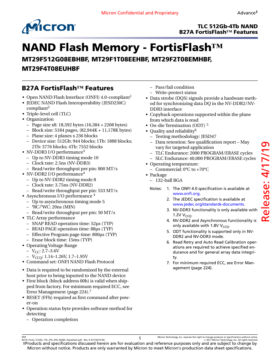
Micron Confidential and Proprietary Advance‡ TLC 512Gb-4Tb NAND B27A FortisFlash™ Features NAND Flash Memory - FortisFlash™ MT29F512G08EBHBF, MT29F1T08EEHBF, MT29F2T08EMHBF, MT29F4T08EUHBF – Pass/fail condition – Write-protect status • Data strobe (DQS) signals provide a hardware meth- od for synchronizing data DQ in the NV-DDR2/NV- DDR3 interface • Copyback operations supported within the plane from which data is read • On-die Termination (ODT) 5 • Quality and reliability6 – Testing methodology: JESD47 – Data retention: See qualification report – May vary for targeted application – TLC Endurance: 2000 PROGRAM/ERASE cycles – SLC Endurance: 40,000 PROGRAM/ERASE cycles • Operating temperature: – Commercial: 0°C to +70°C • Package – 132-ball BGA Notes: 1. The ONFI 4.0 specification is available at www.onfi.org. 2. The JEDEC specification is available at www.jedec.org/standards-documents. 3. NV-DDR3 functionality is only available with 1.2V VCCQ. 4. NV-DDR2 and Asynchronous functionality is only available with 1.8V VCCQ. 5. ODT functionality is supported only in NV- DDR2 and NV-DDR3 mode. 6. Read Retry and Auto Read Calibration oper- ations are required to achieve specified en- durance and for general array data integri- ty. 7. For minimum required ECC, see Error Man- agement (page 224). 9 1 / 7 1 / 4 : e s a e l e R B27A FortisFlash™ Features • Open NAND Flash Interface (ONFI) 4.0-compliant1 • JEDEC NAND Flash Interoperability (JESD230C) compliant2 • Triple-level cell (TLC) • Organization – Page size x8: 18,592 bytes (16,384 + 2208 bytes) – Block size: 5184 pages, (82,944K + 11,178K bytes) – Plane size: 4 planes x 236 blocks – Device size: 512Gb: 944 blocks; 1Tb: 1888 blocks; 2Tb: 3776 blocks; 4Tb: 7552 blocks • NV-DDR3 I/O performance3 – Up to NV-DDR3 timing mode 10 – Clock rate: 2.5ns (NV-DDR3) – Read/write throughput per pin: 800 MT/s • NV-DDR2 I/O performance4 – Up to NV-DDR2 timing mode 8 – Clock rate: 3.75ns (NV-DDR2) – Read/write throughput per pin: 533 MT/s • Asynchronous I/O performance 4 – Up to asynchronous timing mode 5 – tRC/tWC: 20ns (MIN) – Read/write throughput per pin: 50 MT/s • TLC Array performance – SNAP READ operation time: 52µs (TYP) – READ PAGE operation time: 88µs (TYP) – Effective Program page time: 800µs (TYP) – Erase block time: 15ms (TYP) • Operating Voltage Range – VCC: 2.7–3.6V – VCCQ: 1.14–1.26V, 1.7–1.95V • Command set: ONFI NAND Flash Protocol • Data is required to be randomized by the external host prior to being inputted to the NAND device • First block (block address 00h) is valid when ship- ped from factory. For minimum required ECC, see Error Management (page 224).7 • RESET (FFh) required as first command after pow- er-on • Operation status byte provides software method for detecting – Operation completion PDF Micron Technology, Inc. reserves the right to change products or specifications without notice. © 2017 Micron Technology, Inc. All rights reserved. B27A_Fortis_512Gb_1Tb_2Tb_4Tb_NAND_Datasheet.pdf - Rev. K 4/17/2019 EN ‡Products and specifications discussed herein are for evaluation and reference purposes only and are subject to change by Micron without notice. Products are only warranted by Micron to meet Micron's production data sheet specifications. 1
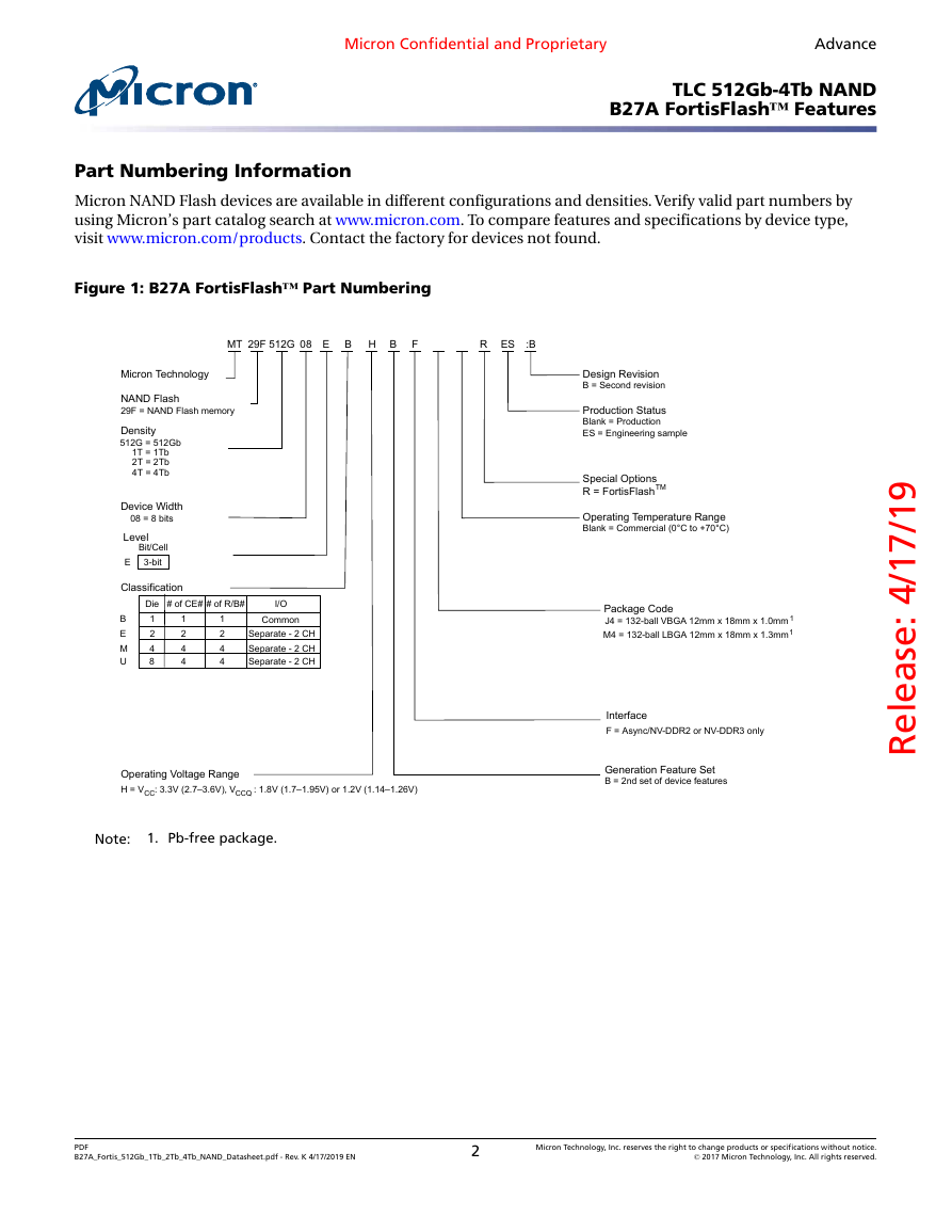
Micron Confidential and Proprietary Advance TLC 512Gb-4Tb NAND B27A FortisFlash™ Features Part Numbering Information Micron NAND Flash devices are available in different configurations and densities. Verify valid part numbers by using Micron’s part catalog search at www.micron.com. To compare features and specifications by device type, visit www.micron.com/products. Contact the factory for devices not found. Figure 1: B27A FortisFlash™ Part Numbering MT 29F 512G 08 E B H B F R ES :B Micron Technology NAND Flash 29F = NAND Flash memory Density 512G = 512Gb 1T = 1Tb 2T = 2Tb 4T = 4Tb Device Width 08 = 8 bits Level E Bit/Cell 3-bit Classification B E M U Die # of CE# # of R/B# 1 2 4 8 1 2 4 4 I/O Common 1 2 Separate - 2 CH 4 Separate - 2 CH 4 Separate - 2 CH Operating Voltage Range H = VCC : 3.3V (2.7–3.6V), V : 1.8V (1.7–1.95V) or 1.2V (1.14–1.26V) CCQ Note: 1. Pb-free package. Design Revision B = Second revision Production Status Blank = Production ES = Engineering sample Special Options R = FortisFlash TM Operating Temperature Range Blank = Commercial (0°C to +70°C) Package Code 1 J4 = 132-ball VBGA 12mm x 18mm x 1.0mm M4 = 132-ball LBGA 12mm x 18mm x 1.3mm1 Interface F = Async/NV-DDR2 or NV-DDR3 only Generation Feature Set B = 2nd set of device features 9 1 / 7 1 / 4 : e s a e l e R PDF B27A_Fortis_512Gb_1Tb_2Tb_4Tb_NAND_Datasheet.pdf - Rev. K 4/17/2019 EN 2 Micron Technology, Inc. reserves the right to change products or specifications without notice. © 2017 Micron Technology, Inc. All rights reserved.
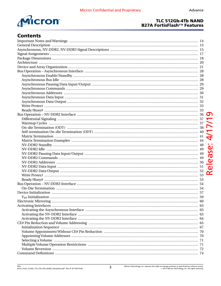
Micron Confidential and Proprietary Advance TLC 512Gb-4Tb NAND B27A FortisFlash™ Features Contents Important Notes and Warnings ....................................................................................................................... 14 General Description ....................................................................................................................................... 15 Asynchronous, NV-DDR2, NV-DDR3 Signal Descriptions ................................................................................. 15 Signal Assignments ......................................................................................................................................... 17 Package Dimensions ....................................................................................................................................... 18 Architecture ................................................................................................................................................... 20 Device and Array Organization ........................................................................................................................ 21 Bus Operation – Asynchronous Interface ......................................................................................................... 28 Asynchronous Enable/Standby ................................................................................................................... 28 Asynchronous Bus Idle ............................................................................................................................... 28 Asynchronous Pausing Data Input/Output .................................................................................................. 29 Asynchronous Commands .......................................................................................................................... 29 Asynchronous Addresses ............................................................................................................................ 30 Asynchronous Data Input ........................................................................................................................... 31 Asynchronous Data Output ......................................................................................................................... 32 Write Protect .............................................................................................................................................. 33 Ready/Busy# .............................................................................................................................................. 33 Bus Operation – NV-DDR2 Interface ................................................................................................................ 36 Differential Signaling .................................................................................................................................. 37 Warmup Cycles .......................................................................................................................................... 37 On-die Termination (ODT) ......................................................................................................................... 38 Self-termination On-die Termination (ODT) ................................................................................................ 40 Matrix Termination .................................................................................................................................... 41 Matrix Termination Examples ..................................................................................................................... 44 NV-DDR2 Standby ...................................................................................................................................... 48 NV-DDR2 Idle ............................................................................................................................................ 49 NV-DDR2 Pausing Data Input/Output ......................................................................................................... 49 NV-DDR2 Commands ................................................................................................................................. 49 NV-DDR2 Addresses ................................................................................................................................... 50 NV-DDR2 Data Input .................................................................................................................................. 51 NV-DDR2 Data Output ............................................................................................................................... 52 Write Protect .............................................................................................................................................. 53 Ready/Busy# .............................................................................................................................................. 53 Bus Operation – NV-DDR3 Interface ................................................................................................................ 54 On-Die Termination ................................................................................................................................... 54 Device Initialization ....................................................................................................................................... 57 VPP Initialization ......................................................................................................................................... 59 Electronic Mirroring ....................................................................................................................................... 60 Activating Interfaces ....................................................................................................................................... 63 Activating the Asynchronous Interface ........................................................................................................ 63 Activating the NV-DDR2 Interface ............................................................................................................... 63 Activating the NV-DDR3 Interface ............................................................................................................... 64 CE# Pin Reduction and Volume Addressing ..................................................................................................... 65 Initialization Sequence ............................................................................................................................... 67 Volume Appointment Without CE# Pin Reduction ....................................................................................... 70 Appointing Volume Addresses ..................................................................................................................... 70 Selecting a Volume ..................................................................................................................................... 71 Multiple Volume Operation Restrictions ...................................................................................................... 71 Volume Reversion ....................................................................................................................................... 72 Command Definitions .................................................................................................................................... 74 PDF B27A_Fortis_512Gb_1Tb_2Tb_4Tb_NAND_Datasheet.pdf - Rev. K 4/17/2019 EN 3 Micron Technology, Inc. reserves the right to change products or specifications without notice. © 2017 Micron Technology, Inc. All rights reserved. 9 1 / 7 1 / 4 : e s a e l e R
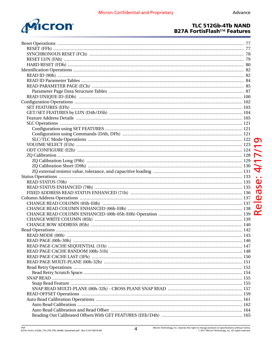
Micron Confidential and Proprietary Advance TLC 512Gb-4Tb NAND B27A FortisFlash™ Features Reset Operations ............................................................................................................................................ 77 RESET (FFh) ............................................................................................................................................... 77 SYNCHRONOUS RESET (FCh) .................................................................................................................... 78 RESET LUN (FAh) ....................................................................................................................................... 79 HARD RESET (FDh) .................................................................................................................................... 80 Identification Operations ................................................................................................................................ 82 READ ID (90h) ............................................................................................................................................ 82 READ ID Parameter Tables .......................................................................................................................... 84 READ PARAMETER PAGE (ECh) .................................................................................................................. 85 Parameter Page Data Structure Tables ..................................................................................................... 87 READ UNIQUE ID (EDh) ........................................................................................................................... 100 Configuration Operations .............................................................................................................................. 102 SET FEATURES (EFh) ................................................................................................................................. 103 GET/SET FEATURES by LUN (D4h/D5h) .................................................................................................... 104 Feature Address Details ............................................................................................................................. 105 SLC Operations ......................................................................................................................................... 121 Configuration using SET FEATURES ....................................................................................................... 121 Configuration using Commands (DAh, DFh) .......................................................................................... 121 SLC/TLC Mode Operations .................................................................................................................... 122 VOLUME SELECT (E1h) ............................................................................................................................. 123 ODT CONFIGURE (E2h) ............................................................................................................................ 124 ZQ Calibration ........................................................................................................................................... 128 ZQ Calibration Long (F9h) ..................................................................................................................... 129 ZQ Calibration Short (D9h) .................................................................................................................... 130 ZQ external resistor value, tolerance, and capacitive loading ................................................................... 131 Status Operations .......................................................................................................................................... 133 READ STATUS (70h) .................................................................................................................................. 135 READ STATUS ENHANCED (78h) ............................................................................................................... 135 FIXED ADDRESS READ STATUS ENHANCED (71h) .................................................................................... 136 Column Address Operations .......................................................................................................................... 137 CHANGE READ COLUMN (05h-E0h) ......................................................................................................... 137 CHANGE READ COLUMN ENHANCED (06h-E0h) ...................................................................................... 138 CHANGE READ COLUMN ENHANCED (00h-05h-E0h) Operation ............................................................... 139 CHANGE WRITE COLUMN (85h) ............................................................................................................... 139 CHANGE ROW ADDRESS (85h) .................................................................................................................. 140 Read Operations ............................................................................................................................................ 142 READ MODE (00h) .................................................................................................................................... 145 READ PAGE (00h-30h) ............................................................................................................................... 146 READ PAGE CACHE SEQUENTIAL (31h) ..................................................................................................... 147 READ PAGE CACHE RANDOM (00h-31h) ................................................................................................... 148 READ PAGE CACHE LAST (3Fh) ................................................................................................................. 150 READ PAGE MULTI-PLANE (00h-32h) ........................................................................................................ 151 Read Retry Operations ............................................................................................................................... 152 Read Retry Scratch Space ....................................................................................................................... 154 SNAP READ ............................................................................................................................................... 155 Snap Read Feature ................................................................................................................................. 155 SNAP READ MULTI-PLANE (00h-32h) - CROSS PLANE SNAP READ ........................................................ 157 READ OFFSET Operations ......................................................................................................................... 159 Auto Read Calibration Operations .............................................................................................................. 161 Auto Read Calibration ............................................................................................................................ 162 Auto Read Calibration and Read Offset ................................................................................................... 164 Reading Out Calibrated Offsets With GET FEATURES (EEh/D4h) ............................................................. 165 PDF B27A_Fortis_512Gb_1Tb_2Tb_4Tb_NAND_Datasheet.pdf - Rev. K 4/17/2019 EN 4 Micron Technology, Inc. reserves the right to change products or specifications without notice. © 2017 Micron Technology, Inc. All rights reserved. 9 1 / 7 1 / 4 : e s a e l e R
Micron Confidential and Proprietary Advance TLC 512Gb-4Tb NAND B27A FortisFlash™ Features Soft Data Read Operations ......................................................................................................................... 166 READ PAGE with SOFT INFORMATION (33h-30h) .................................................................................. 167 SOFT INFORMATION READOUT (36h) .................................................................................................. 168 SOFT INFORMATION READOUT (36h) with the Level Indicator Bit ......................................................... 170 Single Bit Soft Bit Read Operations ............................................................................................................. 175 SINGLE BIT SOFT BIT READ PAGE (00h-34h) ......................................................................................... 177 SINGLE BIT SOFT BIT READ PAGE CACHE RANDOM (00h-38h) ............................................................. 179 Word Line Status Bypass ............................................................................................................................ 182 TLC Two Pass Programming (2-8) ................................................................................................................... 184 PROGRAM PAGE (80h-10h) ........................................................................................................................ 186 PROGRAM PAGE CACHE (80h-15h) ............................................................................................................ 188 PROGRAM PAGE MULTI-PLANE (80h-11h) ................................................................................................ 190 PROGRAM SUSPEND (84h) and PROGRAM RESUME (13h) ......................................................................... 194 Multiple Page Data Entry during Cache Programming ................................................................................. 196 Erase Operations ........................................................................................................................................... 198 ERASE BLOCK (60h-D0h) ........................................................................................................................... 198 ERASE BLOCK MULTI-PLANE (60h-D1h) ................................................................................................... 199 ERASE BLOCK MULTI-PLANE (60h-60h-D0h) ............................................................................................ 199 ERASE SUSPEND (61h) and ERASE RESUME (D2h) .................................................................................... 200 Nested Suspend ............................................................................................................................................ 203 Copyback Operations .................................................................................................................................... 206 COPYBACK READ (00h-35h) ...................................................................................................................... 207 COPYBACK PROGRAM (85h–10h) .............................................................................................................. 209 COPYBACK READ MULTI-PLANE (00h-32h) ............................................................................................... 212 COPYBACK PROGRAM MULTI-PLANE (85h-11h) ....................................................................................... 213 One-Time Programmable (OTP) Operations ................................................................................................... 216 PROGRAM OTP PAGE (80h-10h) ................................................................................................................ 217 PROTECT OTP AREA (80h-10h) .................................................................................................................. 219 READ OTP PAGE (00h-30h) ........................................................................................................................ 220 Multi-Plane Operations ................................................................................................................................. 221 Multi-Plane Addressing ............................................................................................................................. 221 Interleaved Die (Multi-LUN) Operations ......................................................................................................... 222 Error Management ........................................................................................................................................ 224 External Data Randomization .................................................................................................................... 225 Shared Pages - TLC ........................................................................................................................................ 226 Output Drive Impedance ............................................................................................................................... 235 AC Overshoot/Undershoot Specifications ....................................................................................................... 240 Input Slew Rate ............................................................................................................................................. 242 Output Slew Rate ........................................................................................................................................... 250 Power Cycle and Ramp Requirements ............................................................................................................ 252 Electrical Specifications ................................................................................................................................. 253 Package Electrical Specification and Pad Capacitance ................................................................................. 253 Electrical Specifications – DC Characteristics and Operating Conditions (Asynchronous) ................................. 256 Electrical Specifications – DC Characteristics and Operating Conditions (NV-DDR2, NV-DDR3) ....................... 258 Electrical Specifications – DC Characteristics and Operating Conditions (VCCQ) ............................................... 263 Single-Ended Requirements for Differential signals ..................................................................................... 267 Testing Conditions ........................................................................................................................................ 268 Electrical Specifications – AC Characteristics and Operating Conditions (Asynchronous) ................................. 270 Electrical Specifications – AC Characteristics and Operating Conditions (NV-DDR2, NV-DDR3) ........................ 272 Electrical Specifications – Array Characteristics .............................................................................................. 289 Asynchronous Interface Timing Diagrams ...................................................................................................... 293 NV-DDR2 and NV-DDR3 Interface Timing Diagrams ...................................................................................... 301 PDF B27A_Fortis_512Gb_1Tb_2Tb_4Tb_NAND_Datasheet.pdf - Rev. K 4/17/2019 EN 5 Micron Technology, Inc. reserves the right to change products or specifications without notice. © 2017 Micron Technology, Inc. All rights reserved. 9 1 / 7 1 / 4 : e s a e l e R
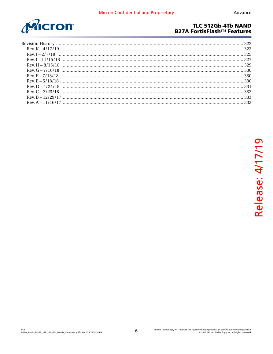
Micron Confidential and Proprietary Advance TLC 512Gb-4Tb NAND B27A FortisFlash™ Features Revision History ............................................................................................................................................ 322 Rev. K – 4/17/19 ......................................................................................................................................... 322 Rev. J – 2/7/19 ........................................................................................................................................... 325 Rev. I – 11/15/18 ........................................................................................................................................ 327 Rev. H – 8/15/18 ........................................................................................................................................ 329 Rev. G – 7/16/18 ........................................................................................................................................ 330 Rev. F – 7/13/18 ......................................................................................................................................... 330 Rev. E – 5/18/18 ......................................................................................................................................... 330 Rev. D – 4/24/18 ........................................................................................................................................ 331 Rev. C – 3/23/18 ......................................................................................................................................... 332 Rev. B – 12/29/17 ....................................................................................................................................... 333 Rev. A – 11/16/17 ....................................................................................................................................... 333 9 1 / 7 1 / 4 : e s a e l e R PDF B27A_Fortis_512Gb_1Tb_2Tb_4Tb_NAND_Datasheet.pdf - Rev. K 4/17/2019 EN 6 Micron Technology, Inc. reserves the right to change products or specifications without notice. © 2017 Micron Technology, Inc. All rights reserved.
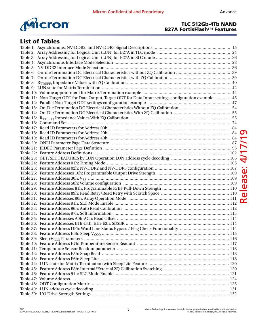
Micron Confidential and Proprietary Advance TLC 512Gb-4Tb NAND B27A FortisFlash™ Features List of Tables Table 1: Asynchronous, NV-DDR2, and NV-DDR3 Signal Descriptions ............................................................. 15 Table 2: Array Addressing for Logical Unit (LUN) for B27A in TLC mode .......................................................... 24 Table 3: Array Addressing for Logical Unit (LUN) for B27A in SLC mode ........................................................... 26 Table 4: Asynchronous Interface Mode Selection ............................................................................................ 28 Table 5: NV-DDR2 Interface Mode Selection ................................................................................................... 36 Table 6: On-die Termination DC Electrical Characteristics without ZQ Calibration ........................................... 39 Table 7: On-die Termination DC Electrical Characteristics with ZQ Calibration ................................................ 39 Table 8: RTT(EFF) Impedance Values with ZQ Calibration .................................................................................. 40 Table 9: LUN state for Matrix Termination ...................................................................................................... 42 Table 10: Volume appointment for Matrix Termination example ..................................................................... 44 Table 11: Non-Target ODT for Data Output, Target ODT for Data Input settings configuration example ............ 45 Table 12: Parallel Non-Target ODT settings configuration example .................................................................. 47 Table 13: On-Die Termination DC Electrical Characteristics Without ZQ Calibration ........................................ 54 Table 14: On-Die Termination DC Electrical Characteristics With ZQ Calibration ............................................. 55 Table 15: RTT(EFF) Impedance Values With ZQ Calibration ............................................................................... 55 Table 16: Command Set ................................................................................................................................. 74 Table 17: Read ID Parameters for Address 00h ................................................................................................ 84 Table 18: Read ID Parameters for Address 20h ................................................................................................ 84 Table 19: Read ID Parameters for Address 40h ................................................................................................ 84 Table 20: ONFI Parameter Page Data Structure ............................................................................................... 87 Table 21: JEDEC Parameter Page Defintion ..................................................................................................... 95 Table 22: Feature Address Definitions ............................................................................................................ 102 Table 23: GET/SET FEATURES by LUN Operation LUN address cycle decoding .............................................. 105 Table 24: Feature Address 01h: Timing Mode ................................................................................................. 105 Table 25: Feature Address 02h: NV-DDR2 and NV-DDR3 configuration ........................................................... 107 Table 26: Feature Addresses 10h: Programmable Output Drive Strength ......................................................... 109 Table 27: Feature Address 30h: VPP ................................................................................................................ 109 Table 28: Feature Address 58h: Volume configuration .................................................................................... 109 Table 29: Feature Addresses 81h: Programmable R/B# Pull-Down Strength ..................................................... 110 Table 30: Feature Address 89h: Read Retry/Read Retry with Scratch Space ...................................................... 110 Table 31: Feature Addresses 90h: Array Operation Mode ................................................................................ 111 Table 32: Feature Address 91h: SLC Mode Enable ........................................................................................... 112 Table 33: Feature Address 96h: Auto Read Calibration .................................................................................... 112 Table 34: Feature Address 97h: Soft Information ............................................................................................ 113 Table 35: Feature Addresses A0h-ACh: Read Offset ......................................................................................... 114 Table 36: Feature Addresses B1h-B4h, E1h-E3h: SBSBR .................................................................................. 114 Table 37: Feature Address DFh: Word Line Status Bypass / Flag Check Functionality ....................................... 114 Table 38: Feature Address E6h: Sleep VCCQ ..................................................................................................... 115 Table 39: Sleep VCCQ Parameters ................................................................................................................... 116 Table 40: Feature Address E7h: Temperature Sensor Readout ......................................................................... 117 Table 41: Temperature Sensor Readout parameter ......................................................................................... 118 Table 42: Feature Address F5h: Snap Read ..................................................................................................... 118 Table 43: Feature Address F6h: Sleep Lite ...................................................................................................... 118 Table 44: LUN state for Matrix Termination with Sleep Lite Feature ................................................................ 120 Table 45: Feature Address F8h: Internal/External ZQ Calibration Switching .................................................... 120 Table 46: Feature Address 91h: SLC Mode Enable ........................................................................................... 121 Table 47: Volume Address ............................................................................................................................. 124 Table 48: ODT Configuration Matrix ............................................................................................................. 125 Table 49: LUN address cycle decoding ........................................................................................................... 131 Table 50: I/O Drive Strength Settings ............................................................................................................. 132 PDF B27A_Fortis_512Gb_1Tb_2Tb_4Tb_NAND_Datasheet.pdf - Rev. K 4/17/2019 EN 7 Micron Technology, Inc. reserves the right to change products or specifications without notice. © 2017 Micron Technology, Inc. All rights reserved. 9 1 / 7 1 / 4 : e s a e l e R
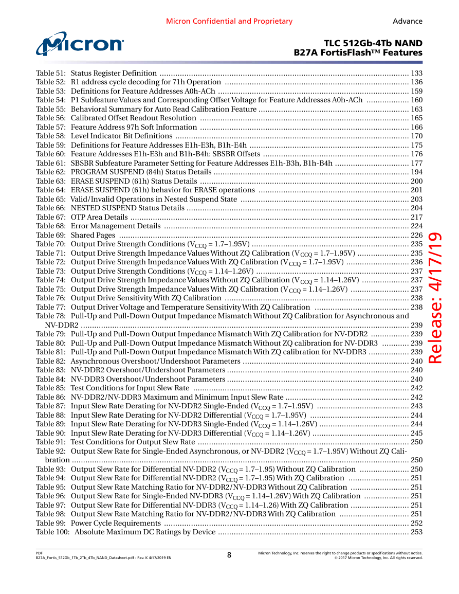
Micron Confidential and Proprietary Advance TLC 512Gb-4Tb NAND B27A FortisFlash™ Features Table 51: Status Register Definition ............................................................................................................... 133 Table 52: R1 address cycle decoding for 71h Operation .................................................................................. 136 Table 53: Definitions for Feature Addresses A0h-ACh ..................................................................................... 159 Table 54: P1 Subfeature Values and Corresponding Offset Voltage for Feature Addresses A0h-ACh ................... 160 Table 55: Behavioral Summary for Auto Read Calibration Feature ................................................................... 163 Table 56: Calibrated Offset Readout Resolution ............................................................................................. 165 Table 57: Feature Address 97h Soft Information ............................................................................................. 166 Table 58: Level Indicator Bit Definitions ........................................................................................................ 170 Table 59: Definitions for Feature Addresses E1h-E3h, B1h-E4h ....................................................................... 175 Table 60: Feature Addresses E1h-E3h and B1h-B4h: SBSBR Offsets ................................................................. 176 Table 61: SBSBR Subfeature Parameter Setting for Feature Addresses E1h-B3h, B1h-B4h ................................. 177 Table 62: PROGRAM SUSPEND (84h) Status Details ....................................................................................... 194 Table 63: ERASE SUSPEND (61h) Status Details ............................................................................................. 200 Table 64: ERASE SUSPEND (61h) behavior for ERASE operations ................................................................... 201 Table 65: Valid/Invalid Operations in Nested Suspend State ........................................................................... 203 Table 66: NESTED SUSPEND Status Details ................................................................................................... 204 Table 67: OTP Area Details ............................................................................................................................ 217 Table 68: Error Management Details ............................................................................................................. 224 Table 69: Shared Pages ................................................................................................................................. 226 Table 70: Output Drive Strength Conditions (VCCQ = 1.7–1.95V) ...................................................................... 235 Table 71: Output Drive Strength Impedance Values Without ZQ Calibration (V CCQ = 1.7–1.95V) ....................... 235 Table 72: Output Drive Strength Impedance Values With ZQ Calibration (V CCQ = 1.7–1.95V) ............................ 236 Table 73: Output Drive Strength Conditions (VCCQ = 1.14–1.26V) .................................................................... 237 Table 74: Output Drive Strength Impedance Values Without ZQ Calibration (V CCQ = 1.14–1.26V) ..................... 237 Table 75: Output Drive Strength Impedance Values With ZQ Calibration (V CCQ = 1.14–1.26V) .......................... 237 Table 76: Output Drive Sensitivity With ZQ Calibration .................................................................................. 238 Table 77: Output Driver Voltage and Temperature Sensitivity With ZQ Calibration .......................................... 238 Table 78: Pull-Up and Pull-Down Output Impedance Mismatch Without ZQ Calibration for Asynchronous and NV-DDR2 .................................................................................................................................................. 239 Table 79: Pull-Up and Pull-Down Output Impedance Mismatch With ZQ Calibration for NV-DDR2 ................. 239 Table 80: Pull-Up and Pull-Down Output Impedance Mismatch Without ZQ calibration for NV-DDR3 ............ 239 Table 81: Pull-Up and Pull-Down Output Impedance Mismatch With ZQ calibration for NV-DDR3 .................. 239 Table 82: Asynchronous Overshoot/Undershoot Parameters .......................................................................... 240 Table 83: NV-DDR2 Overshoot/Undershoot Parameters ................................................................................. 240 Table 84: NV-DDR3 Overshoot/Undershoot Parameters ................................................................................. 240 Table 85: Test Conditions for Input Slew Rate ................................................................................................ 242 Table 86: NV-DDR2/NV-DDR3 Maximum and Minimum Input Slew Rate ....................................................... 242 Table 87: Input Slew Rate Derating for NV-DDR2 Single-Ended (VCCQ = 1.7–1.95V) ......................................... 243 Table 88: Input Slew Rate Derating for NV-DDR2 Differential (VCCQ = 1.7–1.95V) ............................................ 244 Table 89: Input Slew Rate Derating for NV-DDR3 Single-Ended (VCCQ = 1.14–1.26V) ........................................ 244 Table 90: Input Slew Rate Derating for NV-DDR3 Differential (VCCQ = 1.14–1.26V) ........................................... 245 Table 91: Test Conditions for Output Slew Rate .............................................................................................. 250 Table 92: Output Slew Rate for Single-Ended Asynchronous, or NV-DDR2 (VCCQ = 1.7–1.95V) Without ZQ Cali- bration ...................................................................................................................................................... 250 Table 93: Output Slew Rate for Differential NV-DDR2 (VCCQ = 1.7–1.95) Without ZQ Calibration ...................... 250 Table 94: Output Slew Rate for Differential NV-DDR2 (VCCQ = 1.7–1.95) With ZQ Calibration ........................... 251 Table 95: Output Slew Rate Matching Ratio for NV-DDR2/NV-DDR3 Without ZQ Calibration .......................... 251 Table 96: Output Slew Rate for Single-Ended NV-DDR3 (VCCQ = 1.14–1.26V) With ZQ Calibration .................... 251 Table 97: Output Slew Rate for Differential NV-DDR3 (VCCQ = 1.14–1.26) With ZQ Calibration .......................... 251 Table 98: Output Slew Rate Matching Ratio for NV-DDR2/NV-DDR3 With ZQ Calibration ............................... 251 Table 99: Power Cycle Requirements ............................................................................................................. 252 Table 100: Absolute Maximum DC Ratings by Device ..................................................................................... 253 PDF B27A_Fortis_512Gb_1Tb_2Tb_4Tb_NAND_Datasheet.pdf - Rev. K 4/17/2019 EN 8 Micron Technology, Inc. reserves the right to change products or specifications without notice. © 2017 Micron Technology, Inc. All rights reserved. 9 1 / 7 1 / 4 : e s a e l e R
分享到:
收藏