©2016 Toshiba Corporation
2016-12-27
Rev.4.0
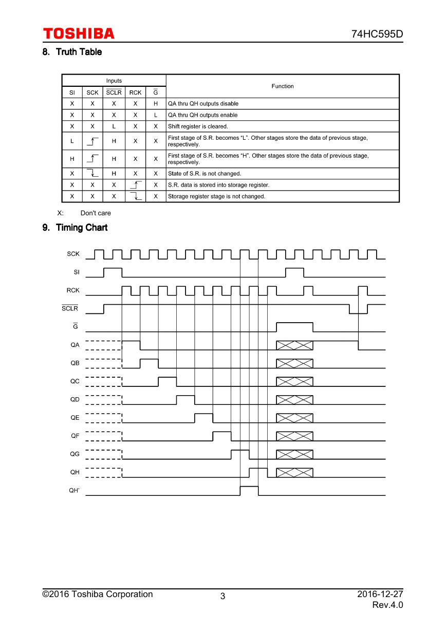
74HC595D1CMOS Digital Integrated CircuitsSilicon Monolithic74HC595D74HC595D74HC595D74HC595DStart of commercial production2016-021. 1. 1. 1. Functional DescriptionFunctional DescriptionFunctional DescriptionFunctional Description•8-Bit Shift Register/Latch (3-state)2. 2. 2. 2. GeneralGeneralGeneralGeneralThe 74HC595D is a high speed 8-BIT SHIFT REGISTER/LATCH fabricated with silicon gate C2MOS technology.It achieve the high speed operation similar to equivalent LSTTL while maintaining the CMOS low powerdissipation.The 74HC595D contains an 8-bit static shift register which feeds an 8-bit storage register.Shift operation is accomplished on the positive going transition of the SCK input. The output register is loadedwith the contents of the shift register on the positive going transition of the RCK input. Since RCK and SCKsignal are independent, parallel outputs can be held stable during the shift operation. And, since the parallel outputs are 3-state, it can be directly connected to 8-bit bus. This register can be used inserial-to-parallel conversion, data receivers, etc.All inputs are equipped with protection circuits against static discharge or transient excess voltage.3. 3. 3. 3. FeaturesFeaturesFeaturesFeatures(1)High speed: fMAX = 55 MHz (typ.) at VCC = 5 V(2)Low power dissipation: ICC = 4.0 µA (max) at Ta = 25(3)Balanced propagation delays: tPLH ≈ tPHL(4)Wide operating voltage range: VCC(opr) = 2.0 V to 6.0 V4. 4. 4. 4. PackagingPackagingPackagingPackagingSOIC16�
©2016 Toshiba Corporation
2016-12-27
Rev.4.0
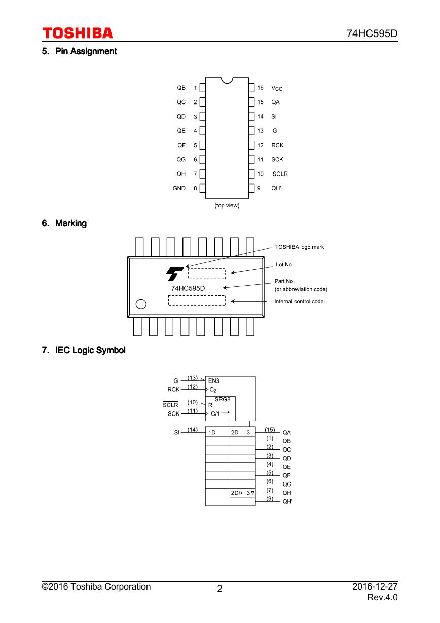
74HC595D25. 5. 5. 5. Pin AssignmentPin AssignmentPin AssignmentPin Assignment6. 6. 6. 6. MarkingMarkingMarkingMarking7. 7. 7. 7. IEC Logic SymbolIEC Logic SymbolIEC Logic SymbolIEC Logic Symbol�
©2016 Toshiba Corporation
2016-12-27
Rev.4.0
74HC595D38. 8. 8. 8. Truth TableTruth TableTruth TableTruth TableX:Don't care 9. 9. 9. 9. Timing ChartTiming ChartTiming ChartTiming Chart�
©2016 Toshiba Corporation
2016-12-27
Rev.4.0
74HC595D410. 10. 10. 10. System DiagramSystem DiagramSystem DiagramSystem Diagram11. 11. 11. 11. Absolute Maximum Ratings (Note)Absolute Maximum Ratings (Note)Absolute Maximum Ratings (Note)Absolute Maximum Ratings (Note)CharacteristicsSupply voltageInput voltageOutput voltageInput diode currentOutput diode currentOutput current (QH')Output current (QA to QH)VCC/ground currentPower dissipationStorage temperatureSymbolVCCVINVOUTIIKIOKIOUTICCPDTstgNote(Note 1)Rating-0.5 to 7.0-0.5 to VCC + 0.5-0.5 to VCC + 0.5±20±20±25±35±75500-65 to 150UnitVVVmAmAmAmAmWNote:Exceeding any of the absolute maximum ratings, even briefly, lead to deterioration in IC performance or evendestruction.Using continuously under heavy loads (e.g. the application of high temperature/current/voltage and thesignificant change in temperature, etc.) may cause this product to decrease in the reliability significantly evenif the operating conditions (i.e. operating temperature/current/voltage, etc.) are within the absolute maximumratings and the operating ranges.Please design the appropriate reliability upon reviewing the Toshiba Semiconductor Reliability Handbook(“Handling Precautions”/“Derating Concept and Methods”) and individual reliability data (i.e. reliability test reportand estimated failure rate, etc).Note 1:PD derates linearly with -8 mW/ above 85 �
©2016 Toshiba Corporation
2016-12-27
Rev.4.0
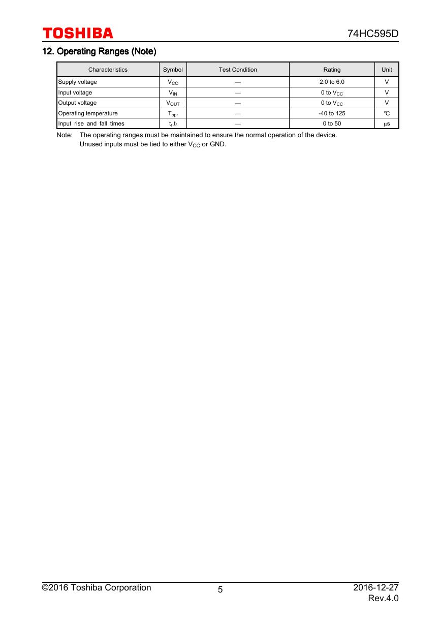
74HC595D512. 12. 12. 12. Operating Ranges (Note)Operating Ranges (Note)Operating Ranges (Note)Operating Ranges (Note)CharacteristicsSupply voltageInput voltageOutput voltageOperating temperatureInput rise and fall timesSymbolVCCVINVOUTToprtr,tfTest ConditionRating2.0 to 6.00 to VCC0 to VCC-40 to 1250 to 50UnitVVVµsNote:The operating ranges must be maintained to ensure the normal operation of the device.Unused inputs must be tied to either VCC or GND.�
©2016 Toshiba Corporation
2016-12-27
Rev.4.0
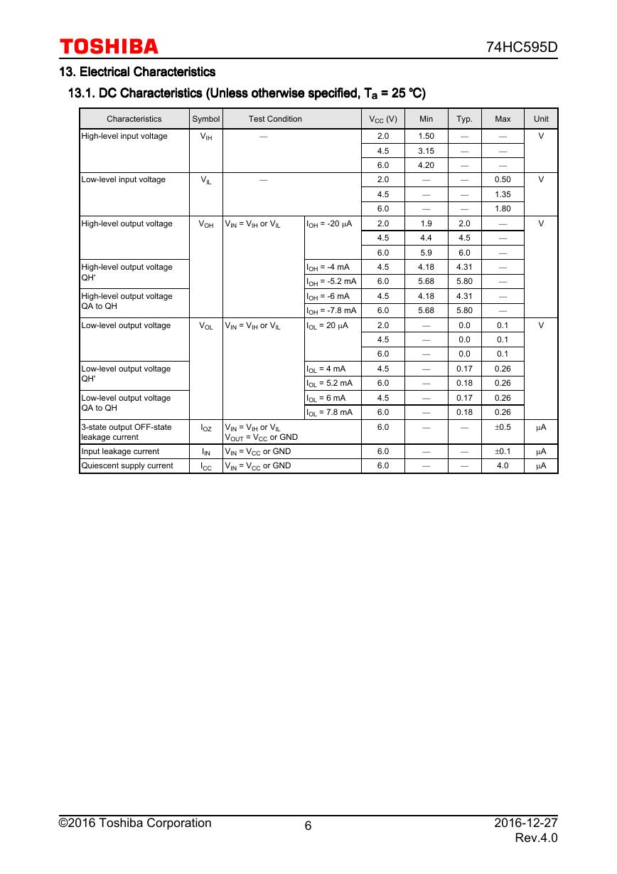
74HC595D613. 13. 13. 13. Electrical CharacteristicsElectrical CharacteristicsElectrical CharacteristicsElectrical Characteristics13.1. 13.1. 13.1. 13.1. DC Characteristics (Unless otherwise specified, TDC Characteristics (Unless otherwise specified, TDC Characteristics (Unless otherwise specified, TDC Characteristics (Unless otherwise specified, Taaaa = 25 = 25 = 25 = 25 ))))CharacteristicsHigh-level input voltageLow-level input voltageHigh-level output voltageHigh-level output voltageQH'High-level output voltageQA to QHLow-level output voltageLow-level output voltageQH'Low-level output voltageQA to QH3-state output OFF-stateleakage currentInput leakage currentQuiescent supply currentSymbolVIHVILVOHVOLIOZIINICCTest ConditionVIN = VIH or VILVIN = VIH or VILVIN = VIH or VILVOUT = VCC or GNDVIN = VCC or GNDVIN = VCC or GNDIOH = -20 µAIOH = -4 mAIOH = -5.2 mAIOH = -6 mAIOH = -7.8 mAIOL = 20 µAIOL = 4 mAIOL = 5.2 mAIOL = 6 mAIOL = 7.8 mAVCC (V)2.04.56.02.04.56.02.04.56.04.56.04.56.02.04.56.04.56.04.56.06.06.06.0Min1.503.154.201.94.45.94.185.684.185.68Typ.2.04.56.04.315.804.315.800.00.00.00.170.180.170.18Max0.501.351.800.10.10.10.260.260.260.26±0.5±0.14.0UnitVVVVµAµAµA�
©2016 Toshiba Corporation
2016-12-27
Rev.4.0
74HC595D713.2. 13.2. 13.2. 13.2. DC Characteristics (Unless otherwise specified, TDC Characteristics (Unless otherwise specified, TDC Characteristics (Unless otherwise specified, TDC Characteristics (Unless otherwise specified, Taaaa = -40 to 85 = -40 to 85 = -40 to 85 = -40 to 85 ))))CharacteristicsHigh-level input voltageLow-level input voltageHigh-level output voltageHigh-level output voltageQH'High-level output voltageQA to QHLow-level output voltageLow-level output voltageQH'Low-level output voltageQA to QH3-state output OFF-state leakagecurrentInput leakage currentQuiescent supply currentSymbolVIHVILVOHVOLIOZIINICCTest ConditionVIN = VIH or VILVIN = VIH or VILVIN = VIH or VILVOUT = VCC or GNDVIN = VCC or GNDVIN = VCC or GNDIOH = -20 µAIOH = -4 mAIOH = -5.2 mAIOH = -6 mAIOH = -7.8 mAIOL = 20 µAIOL = 4 mAIOL = 5.2 mAIOL = 6 mAIOL = 7.8 mAVCC (V)2.04.56.02.04.56.02.04.56.04.56.04.56.02.04.56.04.56.04.56.06.06.06.0Min1.503.154.201.94.45.94.135.634.135.63Max0.501.351.800.10.10.10.330.330.330.33±5.0±1.040.0UnitVVVVµAµAµA�
©2016 Toshiba Corporation
2016-12-27
Rev.4.0
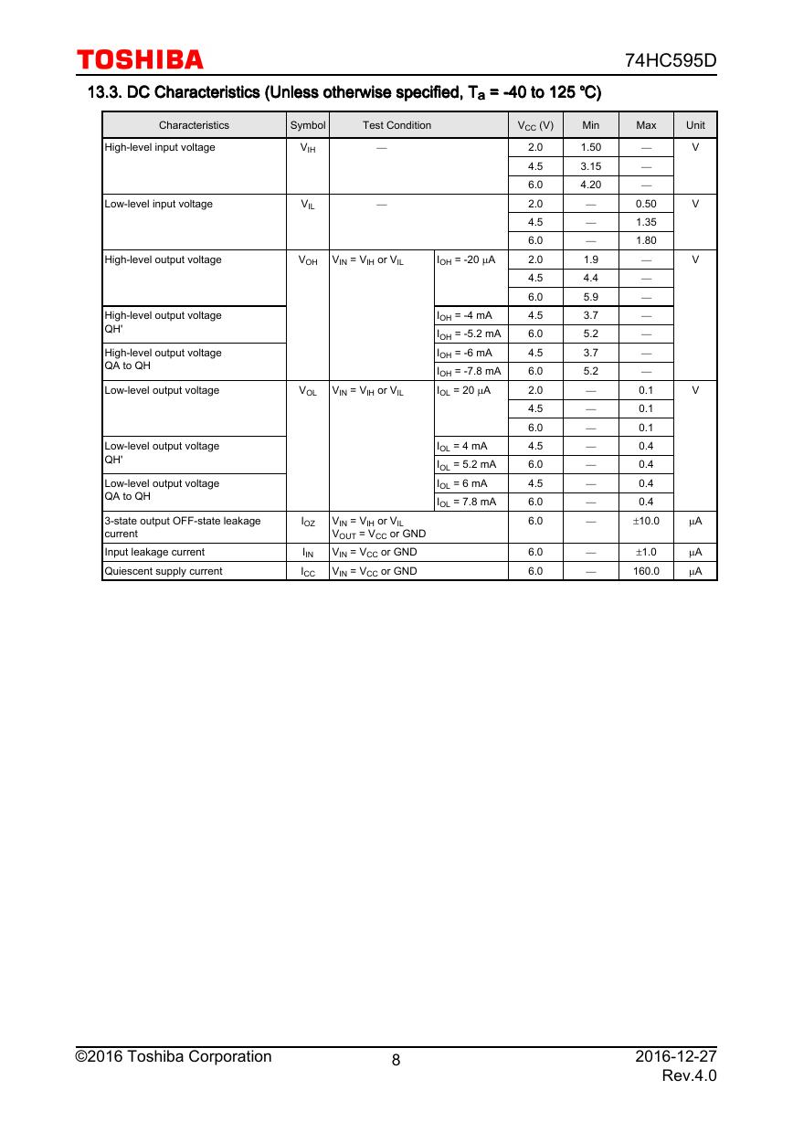
74HC595D813.3. 13.3. 13.3. 13.3. DC Characteristics (Unless otherwise specified, TDC Characteristics (Unless otherwise specified, TDC Characteristics (Unless otherwise specified, TDC Characteristics (Unless otherwise specified, Taaaa = -40 to 125 = -40 to 125 = -40 to 125 = -40 to 125 ))))CharacteristicsHigh-level input voltageLow-level input voltageHigh-level output voltageHigh-level output voltageQH'High-level output voltageQA to QHLow-level output voltageLow-level output voltageQH'Low-level output voltageQA to QH3-state output OFF-state leakagecurrentInput leakage currentQuiescent supply currentSymbolVIHVILVOHVOLIOZIINICCTest ConditionVIN = VIH or VILVIN = VIH or VILVIN = VIH or VILVOUT = VCC or GNDVIN = VCC or GNDVIN = VCC or GNDIOH = -20 µAIOH = -4 mAIOH = -5.2 mAIOH = -6 mAIOH = -7.8 mAIOL = 20 µAIOL = 4 mAIOL = 5.2 mAIOL = 6 mAIOL = 7.8 mAVCC (V)2.04.56.02.04.56.02.04.56.04.56.04.56.02.04.56.04.56.04.56.06.06.06.0Min1.503.154.201.94.45.93.75.23.75.2Max0.501.351.800.10.10.10.40.40.40.4±10.0±1.0160.0UnitVVVVµAµAµA�





 V2版本原理图(Capacitive-Fingerprint-Reader-Schematic_V2).pdf
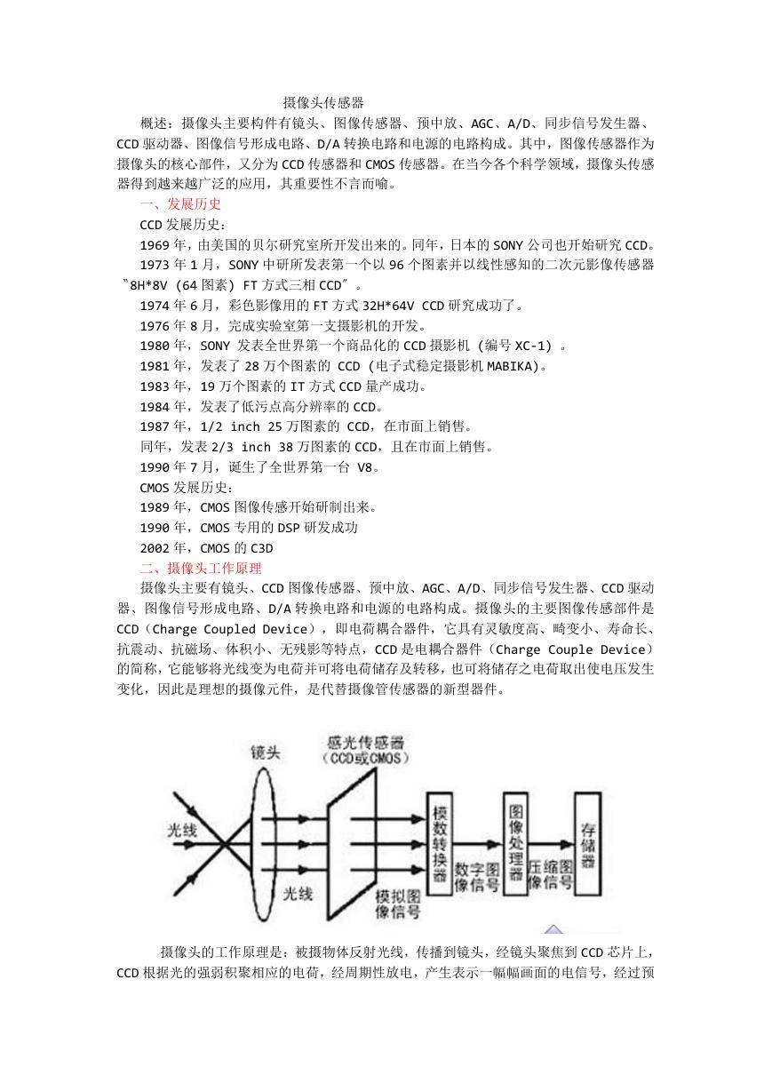 摄像头工作原理.doc
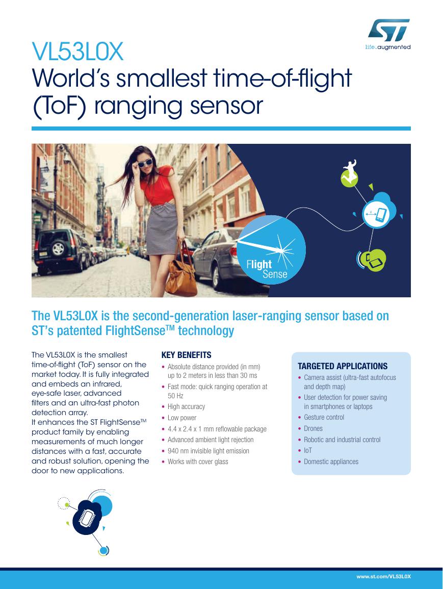 VL53L0X简要说明(En.FLVL53L00216).pdf
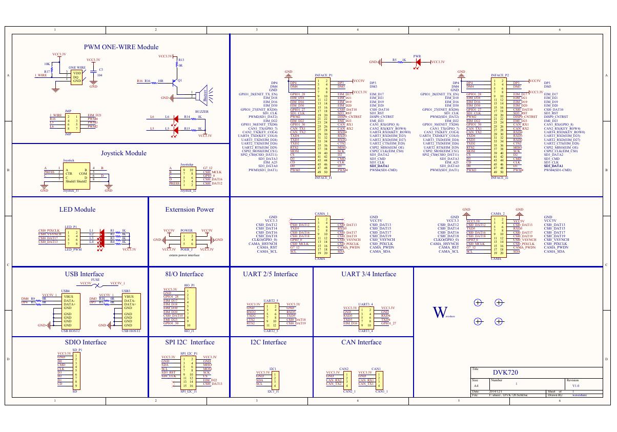 原理图(DVK720-Schematic).pdf
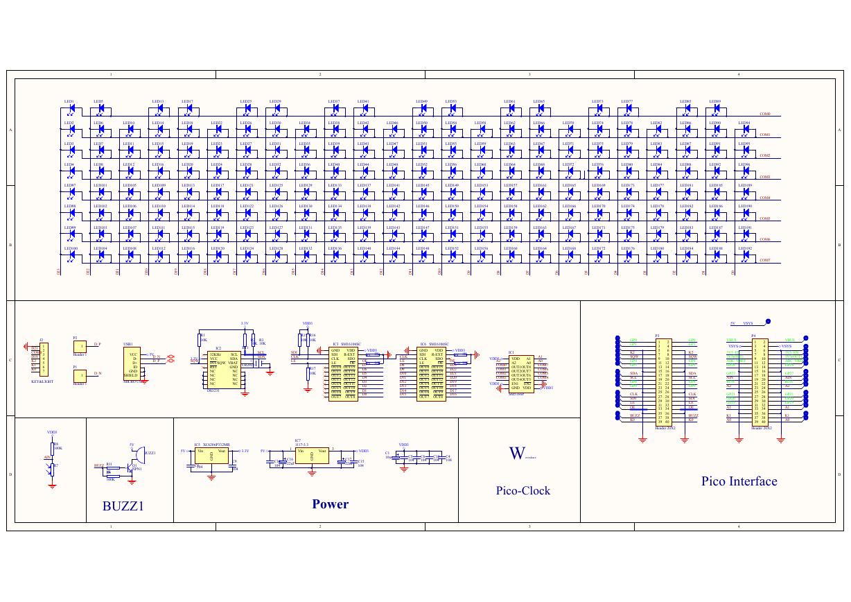 原理图(Pico-Clock-Green-Schdoc).pdf
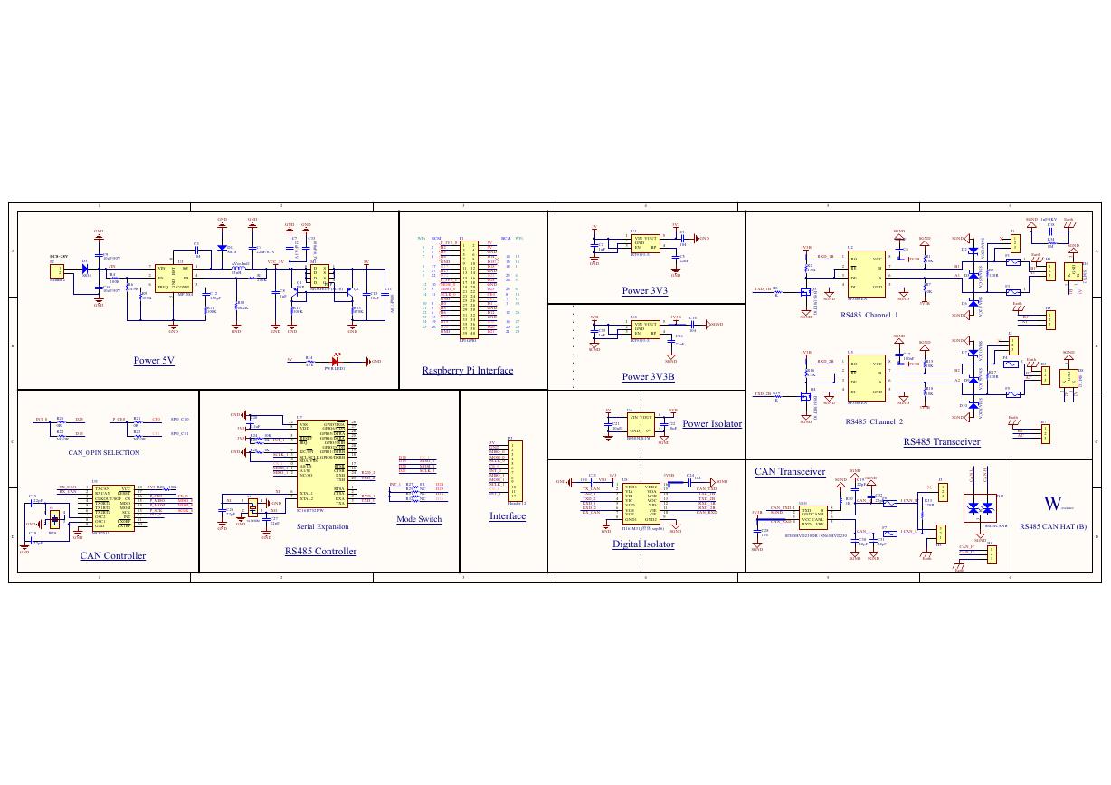 原理图(RS485-CAN-HAT-B-schematic).pdf
 File:SIM7500_SIM7600_SIM7800 Series_SSL_Application Note_V2.00.pdf
 ADS1263(Ads1262).pdf
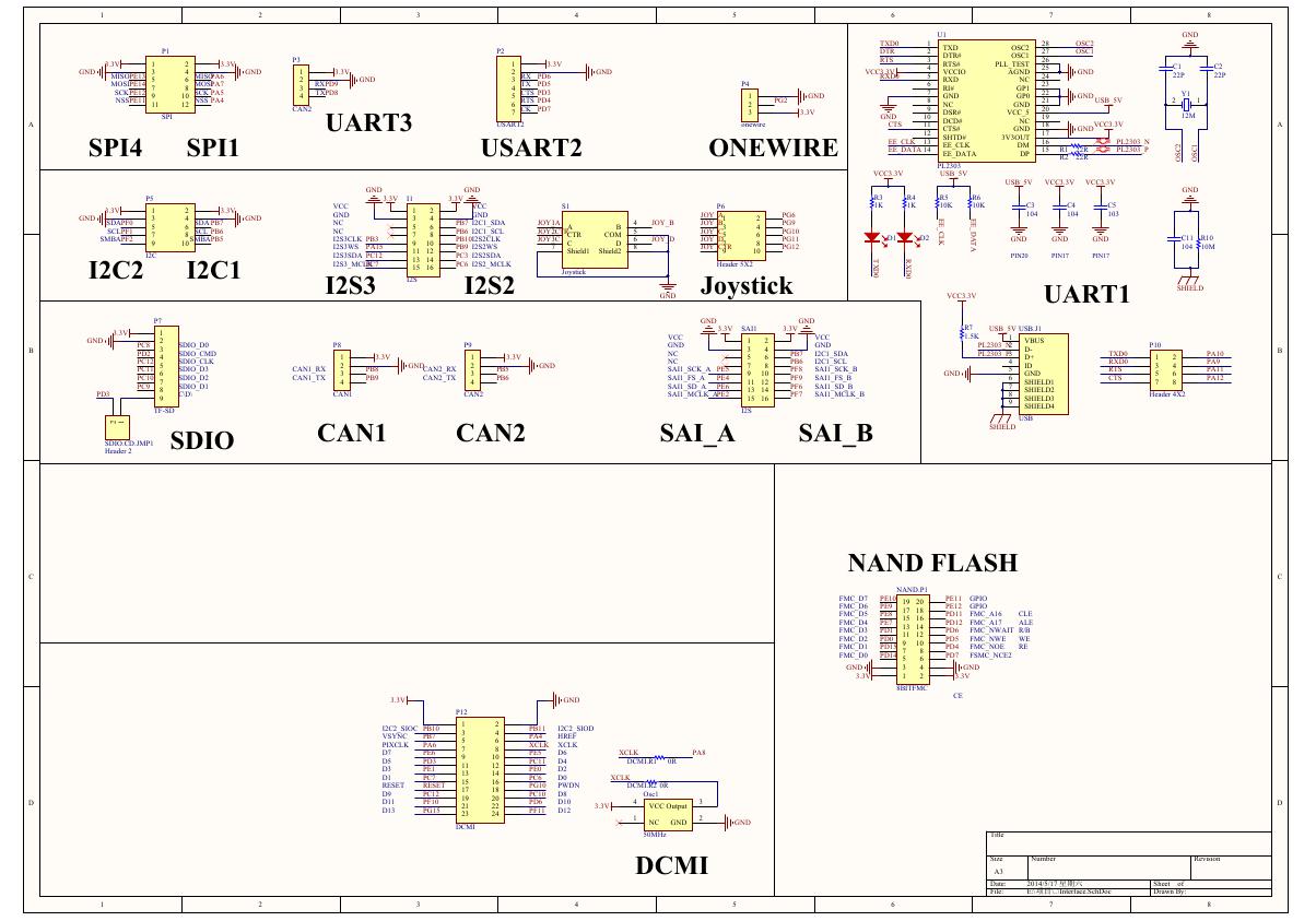 原理图(Open429Z-D-Schematic).pdf
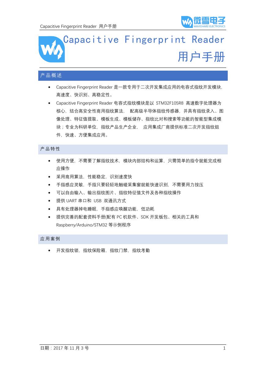 用户手册(Capacitive_Fingerprint_Reader_User_Manual_CN).pdf
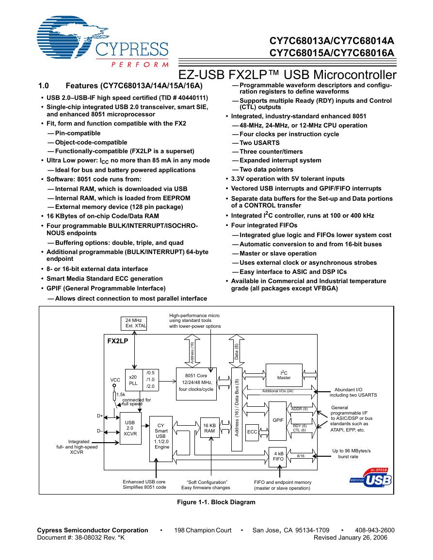 CY7C68013A(英文版)(CY7C68013A).pdf
 TechnicalReference_Dem.pdf