Product
Document
Published by
ams OSRAM Group
�
Datasheet
DS000504
AS7341
11-Channel Multi-Spectral Digital Sensor
v3-00 • 2020-Jun-25
�
Document Feedback
AS7341
Content Guide
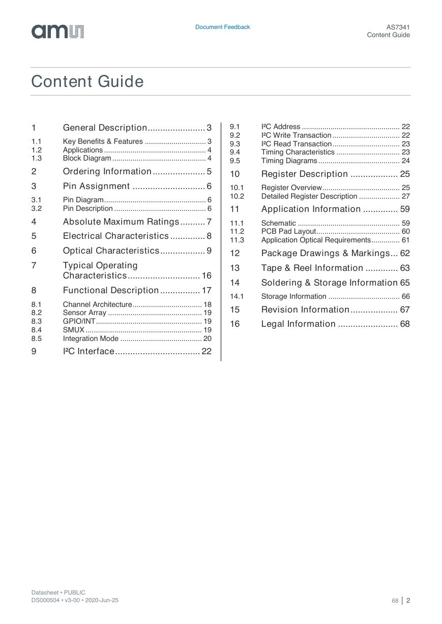
Content Guide
General Description ....................... 3
Key Benefits & Features .............................. 3
Applications .................................................. 4
Block Diagram .............................................. 4
Ordering Information ..................... 5
Pin Assignment ............................. 6
Pin Diagram .................................................. 6
Pin Description ............................................. 6
Absolute Maximum Ratings .......... 7
Electrical Characteristics .............. 8
Optical Characteristics .................. 9
Typical Operating
Characteristics ............................. 16
Functional Description ................ 17
Channel Architecture .................................. 18
Sensor Array .............................................. 19
GPIO/INT .................................................... 19
SMUX ......................................................... 19
Integration Mode ........................................ 20
I²C Interface .................................. 22
9.1
9.2
9.3
9.4
9.5
10
10.1
10.2
11
11.1
11.2
11.3
12
13
14
I²C Address ................................................ 22
I²C Write Transaction ................................. 22
I²C Read Transaction ................................. 23
Timing Characteristics ............................... 23
Timing Diagrams ........................................ 24
Register Description ................... 25
Register Overview ...................................... 25
Detailed Register Description .................... 27
Application Information .............. 59
Schematic .................................................. 59
PCB Pad Layout......................................... 60
Application Optical Requirements .............. 61
Package Drawings & Markings ... 62
Tape & Reel Information ............. 63
Soldering & Storage Information 65
14.1
Storage Information ................................... 66
Revision Information ................... 67
Legal Information ........................ 68
15
16
1
1.1
1.2
1.3
2
3
3.1
3.2
4
5
6
7
8
8.1
8.2
8.3
8.4
8.5
9
Datasheet • PUBLIC
DS000504 • v3-00 • 2020-Jun-25
68 │ 2
�
Document Feedback
AS7341
General Description
1
General Description
The ams AS7341 is an 11-channel spectrometer enabling new consumer, commercial and laboratory
applications including spectral identification, reflection and absorption for color matching, fluid or
reagent analysis, passive ambient light measurement and color calibration. The spectral response is
defined by individual channels covering approximately 350nm to 1000nm with 8 channels centered in
the visible spectrum (VIS), plus one near-infrared (NIR) and a clear channel. The NIR channel in
combination with the other VIS channels may provide information of surrounding ambient light
conditions, including light source detection. Light source detection can be assisted by an integrated
flicker channel that can automatically flag ambient light flicker at 50/60Hz as well as buffer data for
externally calculating other flicker frequencies up to 2kHz.
AS7341 integrates high-precision optical filters onto standard CMOS silicon via nano-optic deposited
interference filter technology. A built-in aperture controls the light entering the sensor array to increase
accuracy. A programmable digital GPIO and LED current controller enable light source and trigger
control, as well as enabling expandability for an added external photodiode. Device control and
spectral data access is implemented through a serial I²C interface. The device is available in an ultra-
low profile package with dimensions of 3.1mm x 2mm x 1mm.
1.1
Key Benefits & Features
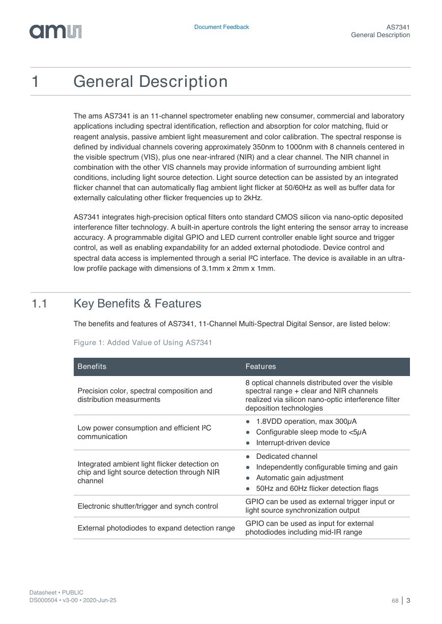
The benefits and features of AS7341, 11-Channel Multi-Spectral Digital Sensor, are listed below:
Figure 1: Added Value of Using AS7341
Benefits
Features
Precision color, spectral composition and
distribution measurments
Low power consumption and efficient I²C
communication
Integrated ambient light flicker detection on
chip and light source detection through NIR
channel
Electronic shutter/trigger and synch control
External photodiodes to expand detection range
8 optical channels distributed over the visible
spectral range + clear and NIR channels
realized via silicon nano-optic interference filter
deposition technologies
● 1.8VDD operation, max 300µA
● Configurable sleep mode to <5µA
● Interrupt-driven device
● Dedicated channel
● Independently configurable timing and gain
● Automatic gain adjustment
● 50Hz and 60Hz flicker detection flags
GPIO can be used as external trigger input or
light source synchronization output
GPIO can be used as input for external
photodiodes including mid-IR range
Datasheet • PUBLIC
DS000504 • v3-00 • 2020-Jun-25
68 │ 3
�
Document Feedback
AS7341
General Description
1.2
Applications
●
●
●
●
High-precision reflective color point and spectral measurements
Fluid color, turbidity or reagent based constituent analysis
Spectral power distribution and passive ambient CCT measurement for home and building
automation
High-end display color management
1.3
Block Diagram
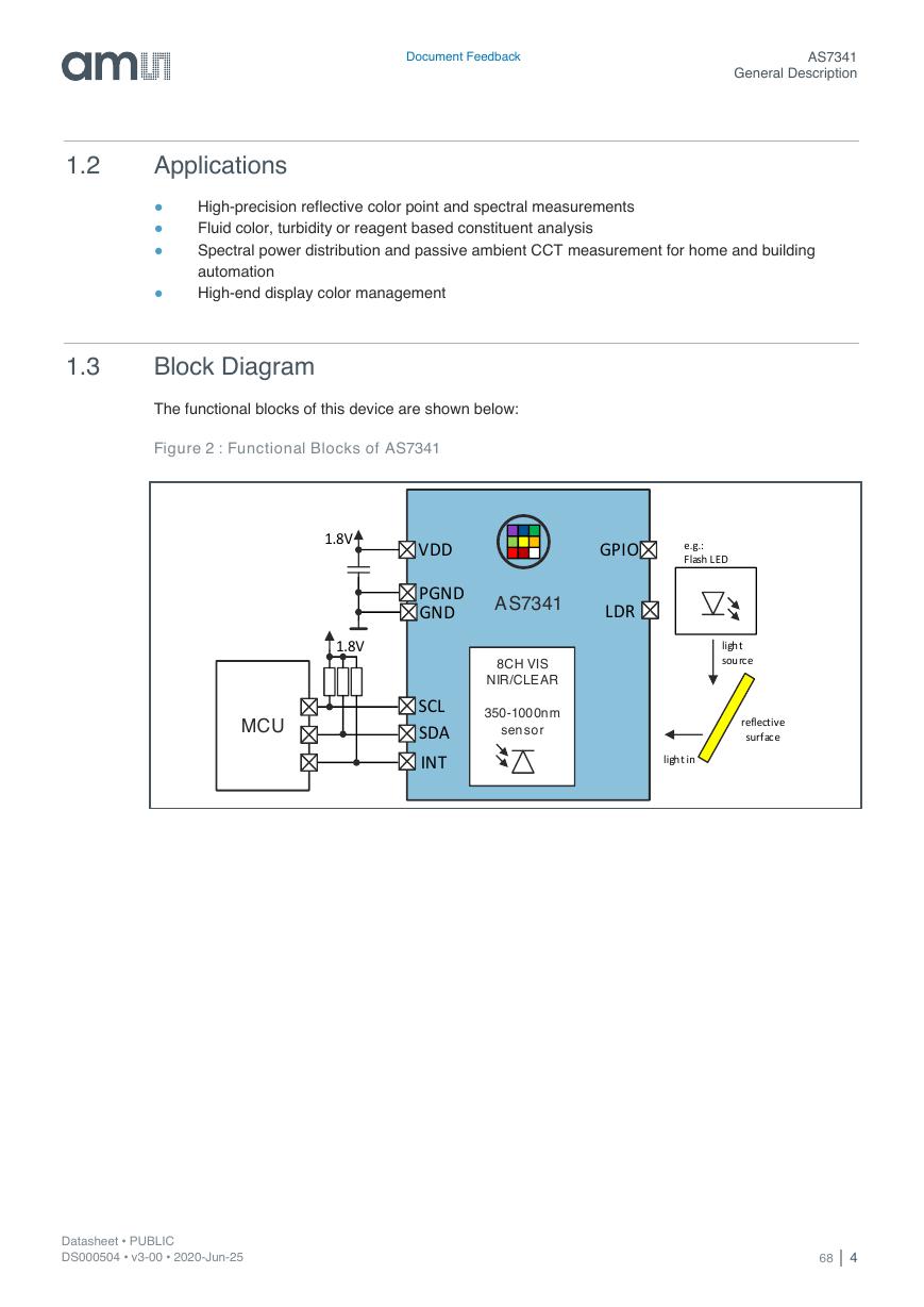
The functional blocks of this device are shown below:
Figure 2 : Functional Blocks of AS7341
68 │ 4
Datasheet • PUBLIC
DS000504 • v3-00 • 2020-Jun-25
AS7341VDDSCLSDA1.8VINTGPIO 8CH VISNIR/CLEAR350-1000nmsensorGNDreflectivesurfacelight inlightsourcee.g.: Flash LEDMCU1.8VLDRPGND�
Document Feedback
AS7341
Ordering Information
2
Ordering Information
Ordering Code
Package
Delivery Form
Delivery Quantity
AS7341-DLGT
OLGA-8
Tape & Reel 13-inch
5000 pcs/reel
AS7341-DLGM
OLGA-8
Tape & Reel 7-inch
500 pcs/reel
68 │ 5
Datasheet • PUBLIC
DS000504 • v3-00 • 2020-Jun-25
�
Document Feedback
AS7341
Pin Assignment
3
Pin Assignment
3.1
Pin Diagram
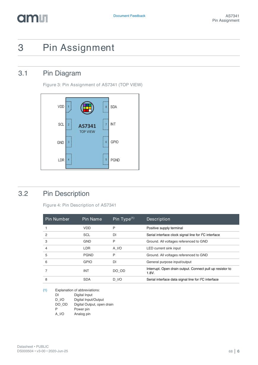
Figure 3: Pin Assignment of AS7341 (TOP VIEW)
3.2
Pin Description
Figure 4: Pin Description of AS7341
Pin Number
Pin Name
Pin Type(1)
Description
1
2
3
4
5
6
7
8
(1)
VDD
SCL
GND
LDR
PGND
GPIO
P
DI
P
Positive supply terminal
Serial interface clock signal line for I2C interface
Ground. All voltages referenced to GND
A_I/O
LED current sink input
P
DI
Ground. All voltages referenced to GND
General purpose input/output
INT
DO_OD
Interrupt. Open drain output. Connect pull up resistor to
1.8V.
SDA
D_I/O
Serial interface data signal line for I2C interface
Explanation of abbreviations:
DI
D_I/O
DO_OD
P
A_I/O
Digital Input
Digital Input/Output
Digital Output, open drain
Power pin
Analog pin
Datasheet • PUBLIC
DS000504 • v3-00 • 2020-Jun-25
68 │ 6
VDDSCLTOP VIEWAS7341INTSDAGPIO23487651GNDLDRPGND�
Document Feedback
AS7341
Absolute Maximum Ratings
4
Absolute Maximum Ratings
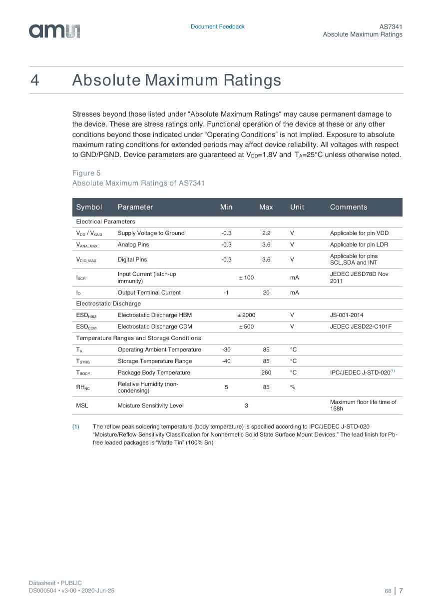
Stresses beyond those listed under “Absolute Maximum Ratings“ may cause permanent damage to
the device. These are stress ratings only. Functional operation of the device at these or any other
conditions beyond those indicated under “Operating Conditions” is not implied. Exposure to absolute
maximum rating conditions for extended periods may affect device reliability. All voltages with respect
to GND/PGND. Device parameters are guaranteed at VDD=1.8V and TA=25°C unless otherwise noted.
Figure 5
Absolute Maximum Ratings of AS7341
Symbol
Parameter
Min
Max
Unit
Comments
Electrical Parameters
VDD / VGND
Supply Voltage to Ground
VANA_MAX
Analog Pins
VDIG_MAX
Digital Pins
-0.3
-0.3
-0.3
2.2
3.6
3.6
ISCR
IO
Input Current (latch-up
immunity)
± 100
Output Terminal Current
-1
20
Electrostatic Discharge
ESDHBM
ESDCDM
Electrostatic Discharge HBM
Electrostatic Discharge CDM
± 2000
± 500
Temperature Ranges and Storage Conditions
TA
TSTRG
TBODY
RHNC
Operating Ambient Temperature
Storage Temperature Range
Package Body Temperature
Relative Humidity (non-
condensing)
-30
-40
5
MSL
Moisture Sensitivity Level
85
85
260
85
3
V
V
V
mA
mA
V
V
°C
°C
°C
%
Applicable for pin VDD
Applicable for pin LDR
Applicable for pins
SCL,SDA and INT
JEDEC JESD78D Nov
2011
JS-001-2014
JEDEC JESD22-C101F
IPC/JEDEC J-STD-020(1)
Maximum floor life time of
168h
(1)
The reflow peak soldering temperature (body temperature) is specified according to IPC/JEDEC J-STD-020
“Moisture/Reflow Sensitivity Classification for Nonhermetic Solid State Surface Mount Devices.” The lead finish for Pb-
free leaded packages is “Matte Tin” (100% Sn)
68 │ 7
Datasheet • PUBLIC
DS000504 • v3-00 • 2020-Jun-25
�





 V2版本原理图(Capacitive-Fingerprint-Reader-Schematic_V2).pdf
 摄像头工作原理.doc
 VL53L0X简要说明(En.FLVL53L00216).pdf
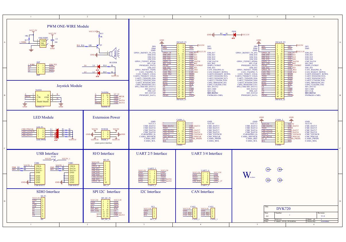 原理图(DVK720-Schematic).pdf
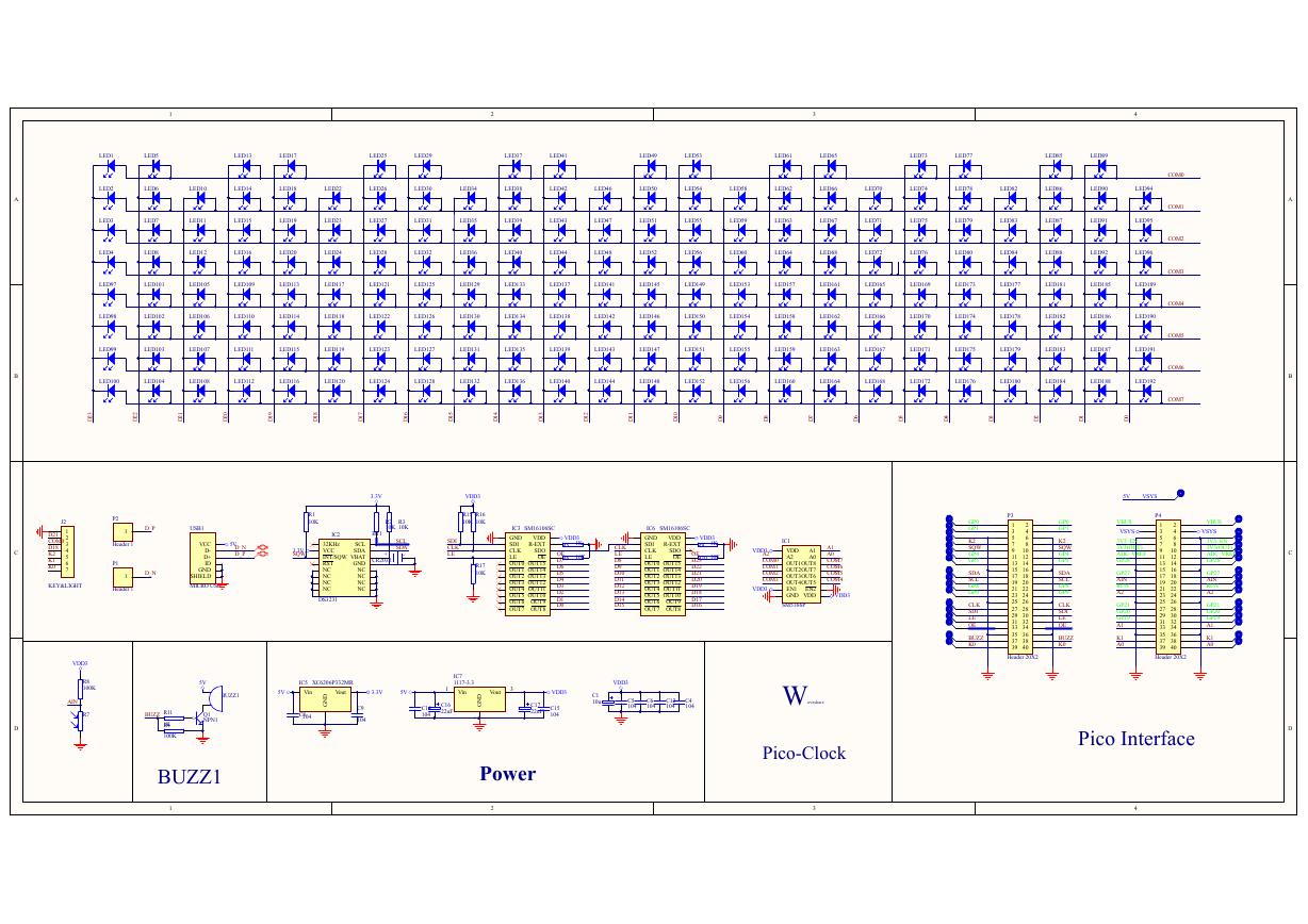 原理图(Pico-Clock-Green-Schdoc).pdf
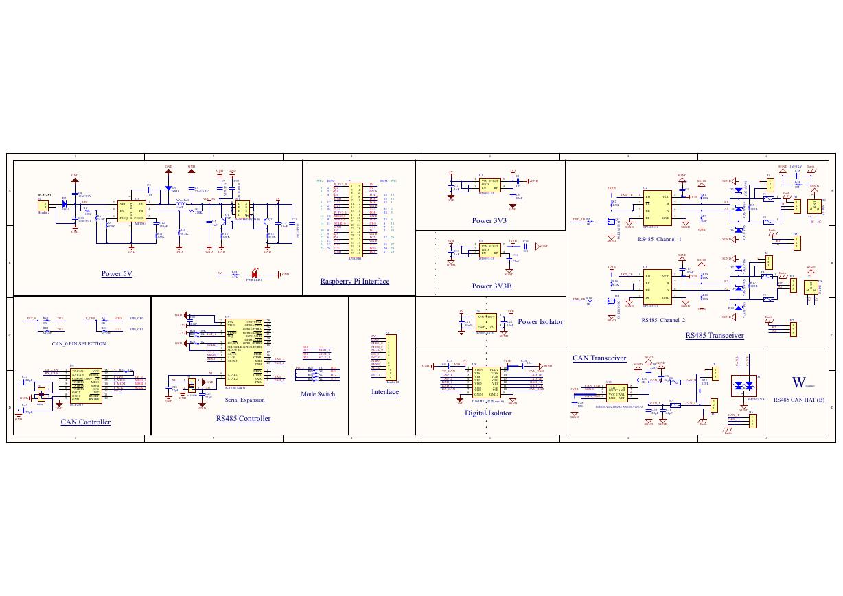 原理图(RS485-CAN-HAT-B-schematic).pdf
 File:SIM7500_SIM7600_SIM7800 Series_SSL_Application Note_V2.00.pdf
 ADS1263(Ads1262).pdf
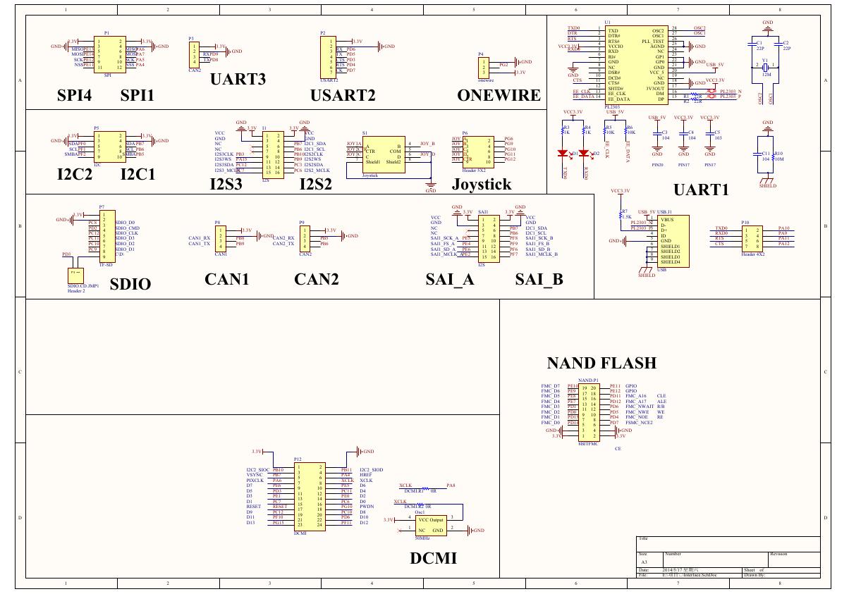 原理图(Open429Z-D-Schematic).pdf
 用户手册(Capacitive_Fingerprint_Reader_User_Manual_CN).pdf
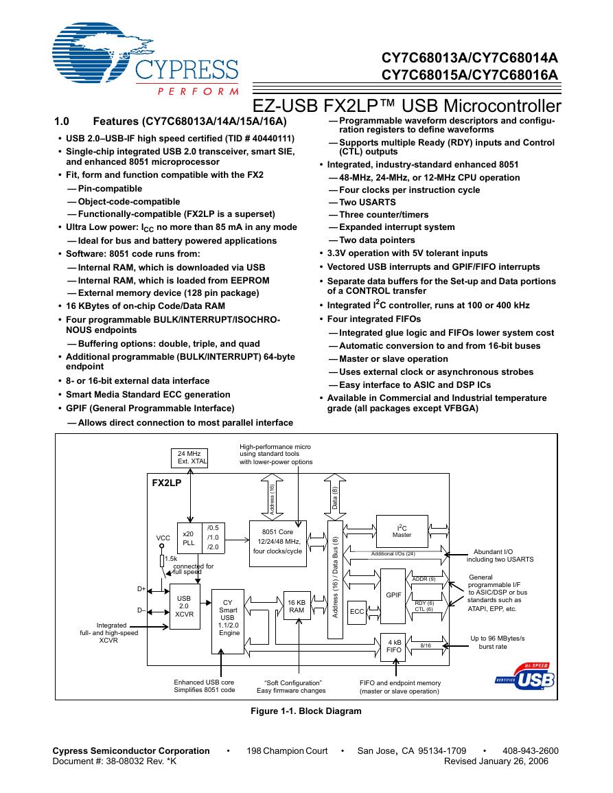 CY7C68013A(英文版)(CY7C68013A).pdf
 TechnicalReference_Dem.pdf