LSF0204x 4-Bits Bidirectional Multi-Voltage Level Translator for Open-Drain and Push-
Pull Application
LSF0204, LSF0204D
SLVSCP5F –JULY 2014–REVISED JANUARY 2019
level
translation
applications
the need for a direction terminal
3 Description
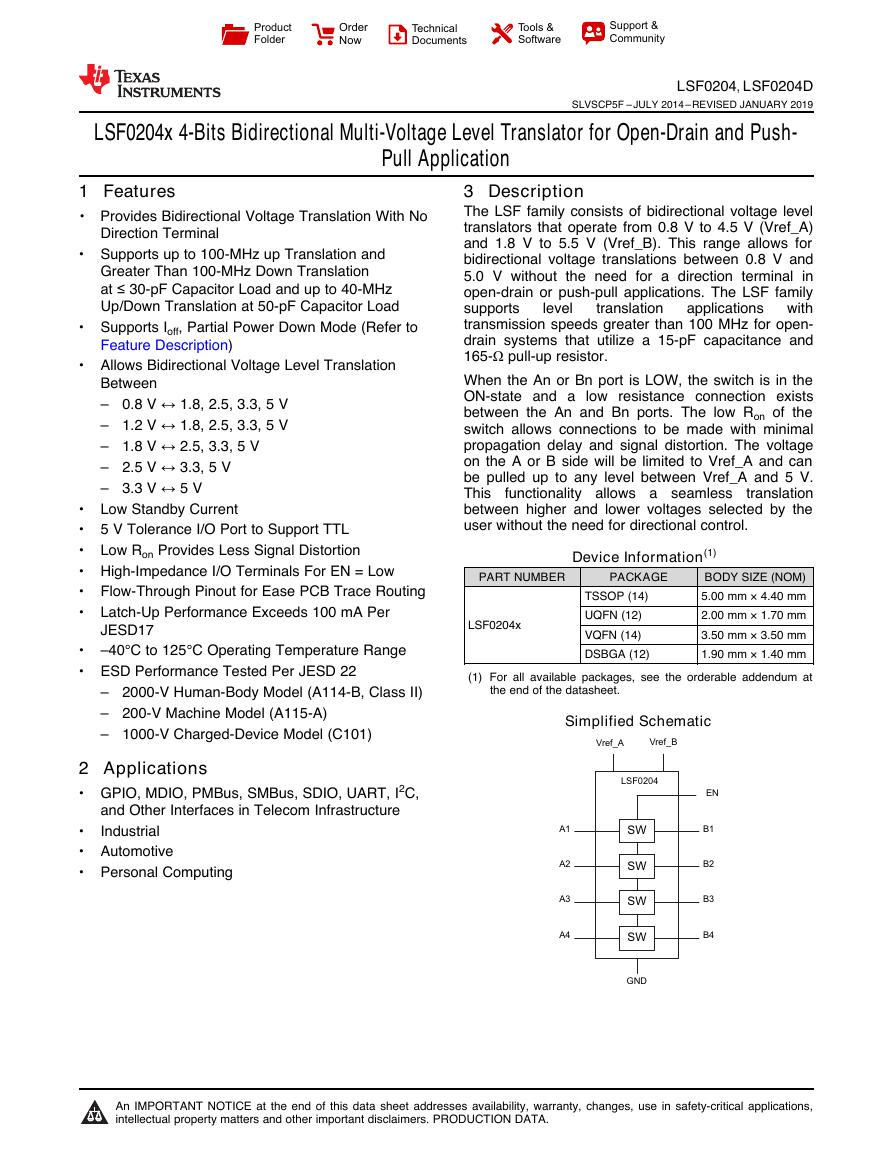
The LSF family consists of bidirectional voltage level
translators that operate from 0.8 V to 4.5 V (Vref_A)
and 1.8 V to 5.5 V (Vref_B). This range allows for
bidirectional voltage translations between 0.8 V and
5.0 V without
in
open-drain or push-pull applications. The LSF family
supports
with
transmission speeds greater than 100 MHz for open-
drain systems that utilize a 15-pF capacitance and
165-Ω pull-up resistor.
When the An or Bn port is LOW, the switch is in the
ON-state and a low resistance connection exists
between the An and Bn ports. The low Ron of the
switch allows connections to be made with minimal
propagation delay and signal distortion. The voltage
on the A or B side will be limited to Vref_A and can
be pulled up to any level between Vref_A and 5 V.
This functionality allows a seamless translation
between higher and lower voltages selected by the
user without the need for directional control.
Device Information(1)
LSF0204x
PACKAGE
PART NUMBER
BODY SIZE (NOM)
5.00 mm × 4.40 mm
2.00 mm × 1.70 mm
3.50 mm × 3.50 mm
1.90 mm × 1.40 mm
(1) For all available packages, see the orderable addendum at
TSSOP (14)
UQFN (12)
VQFN (14)
DSBGA (12)
the end of the datasheet.
Simplified Schematic
1 Features
1• Provides Bidirectional Voltage Translation With No
Direction Terminal
• Supports up to 100-MHz up Translation and
Greater Than 100-MHz Down Translation
at ≤ 30-pF Capacitor Load and up to 40-MHz
Up/Down Translation at 50-pF Capacitor Load
• Supports Ioff, Partial Power Down Mode (Refer to
Feature Description)
• Allows Bidirectional Voltage Level Translation
Between
– 0.8 V ↔ 1.8, 2.5, 3.3, 5 V
– 1.2 V ↔ 1.8, 2.5, 3.3, 5 V
– 1.8 V ↔ 2.5, 3.3, 5 V
– 2.5 V ↔ 3.3, 5 V
– 3.3 V ↔ 5 V
Low Standby Current
5 V Tolerance I/O Port to Support TTL
Low Ron Provides Less Signal Distortion
•
•
•
• High-Impedance I/O Terminals For EN = Low
• Flow-Through Pinout for Ease PCB Trace Routing
•
Latch-Up Performance Exceeds 100 mA Per
JESD17
–40°C to 125°C Operating Temperature Range
•
• ESD Performance Tested Per JESD 22
– 2000-V Human-Body Model (A114-B, Class II)
– 200-V Machine Model (A115-A)
– 1000-V Charged-Device Model (C101)
2 Applications
• GPIO, MDIO, PMBus, SMBus, SDIO, UART, I2C,
and Other Interfaces in Telecom Infrastructure
Industrial
•
• Automotive
• Personal Computing
1
An IMPORTANT NOTICE at the end of this data sheet addresses availability, warranty, changes, use in safety-critical applications,
intellectual property matters and other important disclaimers. PRODUCTION DATA.
Vref_AVref_BENGNDA1A2A3A4B1B2B3B4LSF0204SWSWSWSWProductFolderOrderNowTechnicalDocumentsTools &SoftwareSupport &Community�
LSF0204, LSF0204D
SLVSCP5F –JULY 2014–REVISED JANUARY 2019
www.ti.com
Table of Contents
1
Features.................................................................. 1
2 Applications ........................................................... 1
3 Description ............................................................. 1
4 Revision History..................................................... 2
5 Description (continued)......................................... 3
6 Pin Configuration and Functions ......................... 3
7 Specifications......................................................... 5
7.1 Absolute Maximum Ratings ...................................... 5
7.2 ESD Ratings.............................................................. 5
7.3 Recommended Operating Conditions....................... 5
7.4 Thermal Information ................................................. 5
7.5 Electrical Characteristics........................................... 6
7.6 Switching Characteristics: AC Performance
(Translating Down, 3.3 V to 1.8 V) ........................... 6
7.7 Switching Characteristics: AC Performance
(Translating Down, 3.3 V to 1.2 V) ........................... 7
7.8 Switching Characteristics: AC Performance
(Translating Up, 1.8 V to 3.3 V) ................................ 7
7.9 Switching Characteristics: AC Performance
(Translating Up, 1.2 V to 1.8 V) ................................ 7
7.10 Typical Characteristics............................................ 7
8 Parameter Measurement Information .................. 8
8.1 Load Circuit AC Waveform for Outputs .................... 9
9 Detailed Description ............................................ 10
9.1 Overview ................................................................. 10
9.2 Functional Block Diagram ....................................... 10
9.3 Feature Description................................................. 11
9.4 Device Functional Modes........................................ 11
10 Application and Implementation........................ 12
10.1 Application Information.......................................... 12
10.2 Typical Applications .............................................. 12
11 Power Supply Recommendations ..................... 18
12 Layout................................................................... 18
12.1 Layout Guidelines ................................................. 18
12.2 Layout Example .................................................... 18
13 Device and Documentation Support ................. 20
13.1 Related Links ........................................................ 20
13.2 Community Resources.......................................... 20
13.3 Trademarks ........................................................... 20
13.4 Electrostatic Discharge Caution............................ 20
13.5 Glossary ................................................................ 20
14 Mechanical, Packaging, and Orderable
Information ........................................................... 20
14.1 Package Option Addendum .................................. 21
4 Revision History
NOTE: Page numbers for previous revisions may differ from page numbers in the current version.
Changes from Revision E (December 2018) to Revision F
Page
• Changed location of YZP-package indicator dot to A3 position. ........................................................................................... 3
• Added YZP package to Thermal Information table ................................................................................................................ 5
Changes from Revision D (December 2015) to Revision E
Page
• Changed location of YZP-package A1-pin indicator dot. View is looking through the device, as in an X-ray. ..................... 3
Changes from Revision C (August 2015) to Revision D
Page
• Added Type Column to Pin Functions table........................................................................................................................... 4
• Added Junction Temperatures to Thermal Information table ................................................................................................. 5
Changes from Revision B (April 2015) to Revision C
Page
• Removed "Less than 1.5 ns max propagation delay" from Features. .................................................................................... 1
• Updated "Supports High Speed Translation, Greater Than 100 MHz" bullet in Features. .................................................... 1
Changes from Revision A (December 2014) to Revision B
Page
• Added YZP package to device. ............................................................................................................................................. 1
2
Submit Documentation Feedback
Copyright © 2014–2019, Texas Instruments Incorporated
Product Folder Links: LSF0204 LSF0204D
�
www.ti.com
LSF0204, LSF0204D
SLVSCP5F –JULY 2014–REVISED JANUARY 2019
Changes from Original (November 2014) to Revision A
Page
• Changed From a first page Product Preview To a full datasheet ......................................................................................... 1
• Changed text in the Description From: "transmission speeds greater than 100 Mbps" To: "transmission speeds
greater than 100 MHz" .......................................................................................................................................................... 1
5 Description (continued)
The supply voltage (Vpu#) for each channel may be individually set up with a pull up resistor. For example, CH1
may be used in up-translation mode (1.2 V ↔ 3.3 V) and CH2 in down-translation mode (2.5 V ↔ 1.8 V).
When EN is HIGH, the translator switch is on, and the An I/O is connected to the Bn I/O, respectively, allowing
bidirectional data flow between ports. When EN is LOW, the translator switch is off, and a high-impedance state
exists between ports. The EN input circuit is designed to be supplied by Vref_A. EN must be LOW to ensure the
high-impedance state during power-up or power-down.
Device Comparison Table
PART
NUMBER
LSF0204D
LSF0204D
LSF0204
An
EN
H Place all data pins in 3 state mode
(Hi-Z)
L
Input or output
H Input or output
LSF0204
L
Place all data pins in 3 state mode
(Hi-Z)
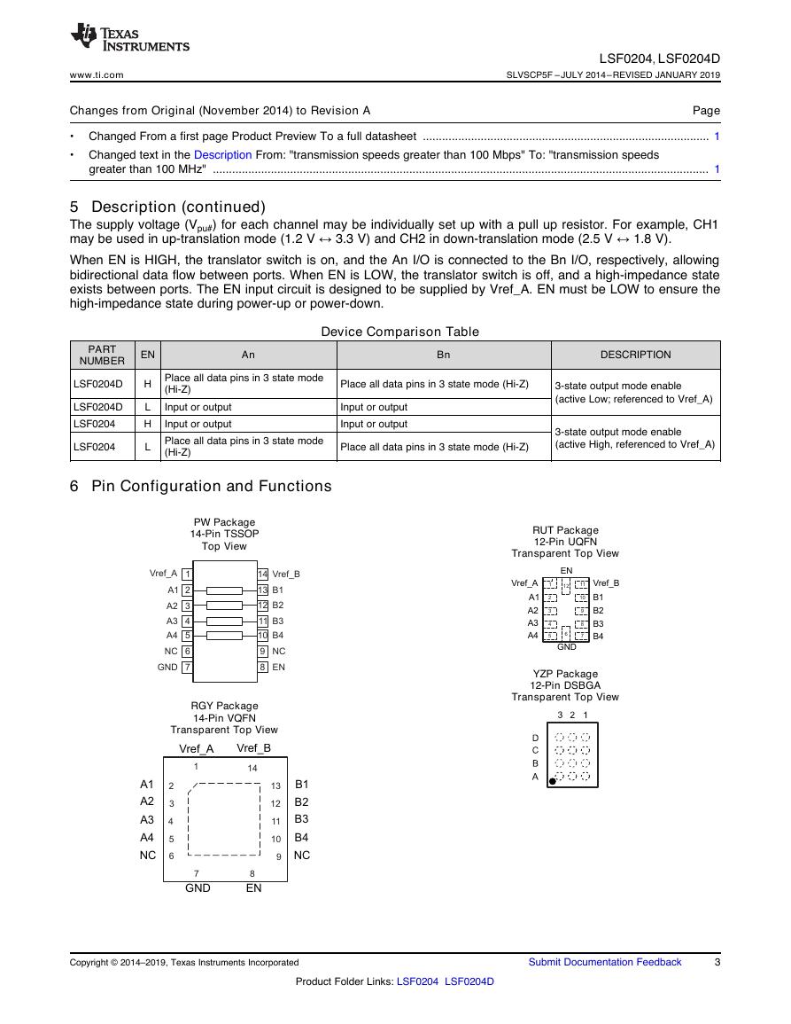
6 Pin Configuration and Functions
PW Package
14-Pin TSSOP
Top View
RGY Package
14-Pin VQFN
Transparent Top View
Bn
DESCRIPTION
Place all data pins in 3 state mode (Hi-Z)
Input or output
Input or output
Place all data pins in 3 state mode (Hi-Z)
3-state output mode enable
(active Low; referenced to Vref_A)
3-state output mode enable
(active High, referenced to Vref_A)
RUT Package
12-Pin UQFN
Transparent Top View
YZP Package
12-Pin DSBGA
Transparent Top View
Copyright © 2014–2019, Texas Instruments Incorporated
Submit Documentation Feedback
3
Product Folder Links: LSF0204 LSF0204D
A2A1A4A3NCVref_BVref_AB2B1B4B3NCENGND11423456789101112131234567891011121314Vref_AA1A2A3A4NCGNDVref_BB1B2B3B4NCENVref_AA1A2A3A4GNDVref_BB1B2B3B4EN123456789101112�
LSF0204, LSF0204D
SLVSCP5F –JULY 2014–REVISED JANUARY 2019
PIN
NO.
PW, RGY
RUT
NAME
Vref_A
A1
A2
A3
A4
NC
GND
EN
NC
B4
B3
B2
B1
Vref_B
1
2
3
4
5
6
7
8
9
10
11
12
13
14
1
2
3
4
5
–
6
12
–
7
8
9
10
11
YZP
B2
A3
B3
C3
D3
–
D2
C2
–
D1
C1
B1
A1
A2
www.ti.com
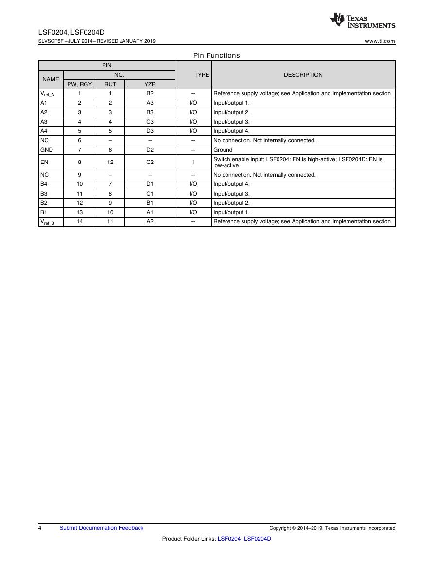
Pin Functions
TYPE
DESCRIPTION
--
I/O
I/O
I/O
I/O
--
--
I
--
I/O
I/O
I/O
I/O
--
Reference supply voltage; see Application and Implementation section
Input/output 1.
Input/output 2.
Input/output 3.
Input/output 4.
No connection. Not internally connected.
Ground
Switch enable input; LSF0204: EN is high-active; LSF0204D: EN is
low-active
No connection. Not internally connected.
Input/output 4.
Input/output 3.
Input/output 2.
Input/output 1.
Reference supply voltage; see Application and Implementation section
4
Submit Documentation Feedback
Copyright © 2014–2019, Texas Instruments Incorporated
Product Folder Links: LSF0204 LSF0204D
�
www.ti.com
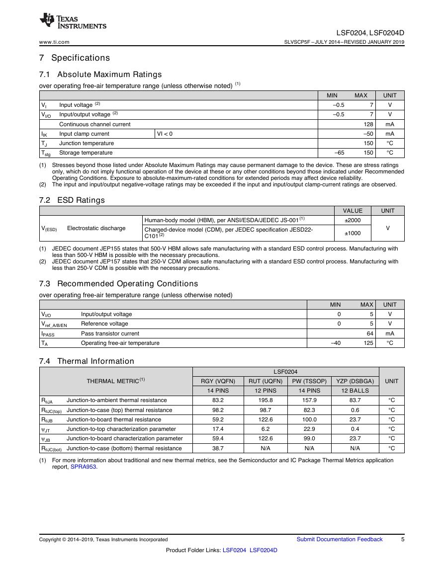
7 Specifications
7.1 Absolute Maximum Ratings
over operating free-air temperature range (unless otherwise noted) (1)
LSF0204, LSF0204D
SLVSCP5F –JULY 2014–REVISED JANUARY 2019
MIN
MAX
UNIT
VI
VI/O
Input voltage (2)
Input/output voltage (2)
Continuous channel current
Input clamp current
Junction temperature
Storage temperature
VI < 0
IIK
TJ
Tstg
(1) Stresses beyond those listed under Absolute Maximum Ratings may cause permanent damage to the device. These are stress ratings
only, which do not imply functional operation of the device at these or any other conditions beyond those indicated under Recommended
Operating Conditions. Exposure to absolute-maximum-rated conditions for extended periods may affect device reliability.
(2) The input and input/output negative-voltage ratings may be exceeded if the input and input/output clamp-current ratings are observed.
–65
–0.5
–0.5
7
7
128
–50
150
150
V
V
mA
mA
°C
°C
7.2 ESD Ratings
V(ESD)
Electrostatic discharge
Human-body model (HBM), per ANSI/ESDA/JEDEC JS-001(1)
Charged-device model (CDM), per JEDEC specification JESD22-
C101(2)
VALUE
±2000
±1000
UNIT
V
(1)
(2)
JEDEC document JEP155 states that 500-V HBM allows safe manufacturing with a standard ESD control process. Manufacturing with
less than 500-V HBM is possible with the necessary precautions.
JEDEC document JEP157 states that 250-V CDM allows safe manufacturing with a standard ESD control process. Manufacturing with
less than 250-V CDM is possible with the necessary precautions.
7.3 Recommended Operating Conditions
over operating free-air temperature range (unless otherwise noted)
VI/O
Vref_A/B/EN
IPASS
TA
Input/output voltage
Reference voltage
Pass transistor current
Operating free-air temperature
7.4 Thermal Information
MIN
0
0
–40
MAX
5
5
64
125
UNIT
V
V
mA
°C
THERMAL METRIC(1)
RGY (VQFN)
RUT (UQFN)
PW (TSSOP)
YZP (DSBGA)
UNIT
LSF0204
14 PINS
12 BALLS
Junction-to-ambient thermal resistance
RθJA
RθJC(top) Junction-to-case (top) thermal resistance
Junction-to-board thermal resistance
RθJB
Junction-to-top characterization parameter
ψJT
Junction-to-board characterization parameter
ψJB
RθJC(bot) Junction-to-case (bottom) thermal resistance
(1) For more information about traditional and new thermal metrics, see the Semiconductor and IC Package Thermal Metrics application
83.2
98.2
59.2
17.4
59.4
38.7
83.7
0.6
23.7
0.4
23.7
N/A
°C
°C
°C
°C
°C
°C
12 PINS
195.8
98.7
122.6
6.2
122.6
N/A
14 PINS
157.9
82.3
100.0
22.9
99.0
N/A
report, SPRA953.
Copyright © 2014–2019, Texas Instruments Incorporated
Submit Documentation Feedback
5
Product Folder Links: LSF0204 LSF0204D
�
LSF0204, LSF0204D
SLVSCP5F –JULY 2014–REVISED JANUARY 2019
www.ti.com
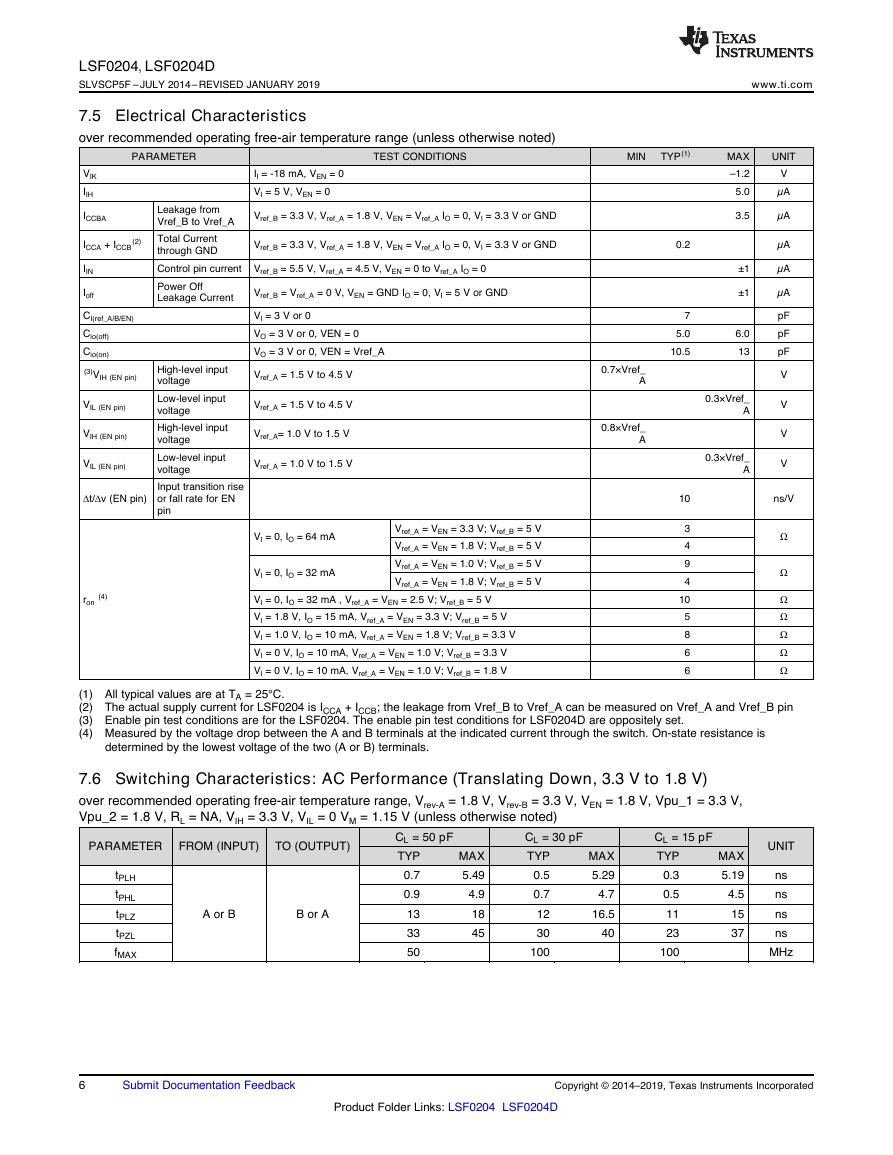
7.5 Electrical Characteristics
over recommended operating free-air temperature range (unless otherwise noted)
PARAMETER
TEST CONDITIONS
MIN
TYP(1)
VIK
IIH
ICCBA
ICCA + ICCB
(2)
IIN
Ioff
CI(ref_A/B/EN)
Cio(off)
Cio(on)
(3)VIH (EN pin)
VIL (EN pin)
VIH (EN pin)
VIL (EN pin)
∆t/∆v (EN pin)
(4)
ron
II = -18 mA, VEN = 0
VI = 5 V, VEN = 0
Vref_B = 3.3 V, Vref_A = 1.8 V, VEN = Vref_A IO = 0, VI = 3.3 V or GND
Vref_B = 3.3 V, Vref_A = 1.8 V, VEN = Vref_A IO = 0, VI = 3.3 V or GND
Leakage from
Vref_B to Vref_A
Total Current
through GND
Control pin current Vref_B = 5.5 V, Vref_A = 4.5 V, VEN = 0 to Vref_A IO = 0
Power Off
Leakage Current
Vref_B = Vref_A = 0 V, VEN = GND IO = 0, VI = 5 V or GND
VI = 3 V or 0
VO = 3 V or 0, VEN = 0
VO = 3 V or 0, VEN = Vref_A
Vref_A = 1.5 V to 4.5 V
Vref_A = 1.5 V to 4.5 V
Vref_A= 1.0 V to 1.5 V
Vref_A = 1.0 V to 1.5 V
High-level input
voltage
Low-level input
voltage
High-level input
voltage
Low-level input
voltage
Input transition rise
or fall rate for EN
pin
VI = 0, IO = 64 mA
VI = 0, IO = 32 mA
Vref_A = VEN = 3.3 V; Vref_B = 5 V
Vref_A = VEN = 1.8 V; Vref_B = 5 V
Vref_A = VEN = 1.0 V; Vref_B = 5 V
Vref_A = VEN = 1.8 V; Vref_B = 5 V
VI = 0, IO = 32 mA , Vref_A = VEN = 2.5 V; Vref_B = 5 V
VI = 1.8 V, IO = 15 mA, Vref_A = VEN = 3.3 V; Vref_B = 5 V
VI = 1.0 V, IO = 10 mA, Vref_A = VEN = 1.8 V; Vref_B = 3.3 V
VI = 0 V, IO = 10 mA, Vref_A = VEN = 1.0 V; Vref_B = 3.3 V
VI = 0 V, IO = 10 mA, Vref_A = VEN = 1.0 V; Vref_B = 1.8 V
0.7×Vref_
A
0.8×Vref_
A
0.2
7
5.0
10.5
10
3
4
9
4
10
5
8
6
6
MAX
–1.2
5.0
3.5
±1
±1
6.0
13
0.3×Vref_
A
0.3×Vref_
A
UNIT
V
µA
µA
µA
µA
µA
pF
pF
pF
V
V
V
V
ns/V
Ω
Ω
Ω
Ω
Ω
Ω
Ω
(1) All typical values are at TA = 25°C.
(2) The actual supply current for LSF0204 is ICCA + ICCB; the leakage from Vref_B to Vref_A can be measured on Vref_A and Vref_B pin
(3) Enable pin test conditions are for the LSF0204. The enable pin test conditions for LSF0204D are oppositely set.
(4) Measured by the voltage drop between the A and B terminals at the indicated current through the switch. On-state resistance is
determined by the lowest voltage of the two (A or B) terminals.
7.6 Switching Characteristics: AC Performance (Translating Down, 3.3 V to 1.8 V)
over recommended operating free-air temperature range, Vrev-A = 1.8 V, Vrev-B = 3.3 V, VEN = 1.8 V, Vpu_1 = 3.3 V,
Vpu_2 = 1.8 V, RL = NA, VIH = 3.3 V, VIL = 0 VM = 1.15 V (unless otherwise noted)
PARAMETER FROM (INPUT)
TO (OUTPUT)
tPLH
tPHL
tPLZ
tPZL
fMAX
A or B
B or A
CL = 50 pF
TYP
0.7
0.9
13
33
50
MAX
5.49
4.9
18
45
CL = 30 pF
TYP
0.5
0.7
12
30
100
MAX
5.29
4.7
16.5
40
CL = 15 pF
TYP
0.3
0.5
11
23
100
MAX
5.19
4.5
15
37
UNIT
ns
ns
ns
ns
MHz
6
Submit Documentation Feedback
Copyright © 2014–2019, Texas Instruments Incorporated
Product Folder Links: LSF0204 LSF0204D
�
www.ti.com
LSF0204, LSF0204D
SLVSCP5F –JULY 2014–REVISED JANUARY 2019
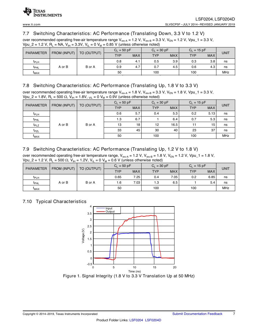
7.7 Switching Characteristics: AC Performance (Translating Down, 3.3 V to 1.2 V)
over recommended operating free-air temperature range Vrev-A = 1.2 V, Vrev-B = 3.3 V, VEN = 1.2 V, Vpu_1 = 3.3 V,
Vpu_2 = 1.2 V, RL = NA, VIH = 3.3V, VIL = 0 VM = 0.85 V (unless otherwise noted)
PARAMETER FROM (INPUT)
TO (OUTPUT)
tPLH
tPHL
fMAX
A or B
B or A
CL = 50 pF
TYP
0.8
0.9
50
MAX
4.1
4.7
CL = 30 pF
TYP
0.5
0.7
100
MAX
3.9
4.5
CL = 15 pF
TYP
0.3
0.6
100
MAX
3.8
4.3
UNIT
ns
ns
MHz
7.8 Switching Characteristics: AC Performance (Translating Up, 1.8 V to 3.3 V)
over recommended operating free-air temperature range Vrev-A = 1.8 V, Vrev-B = 3.3 V, VEN = 1.8 V, Vpu_1 = 3.3 V,
Vpu_2 = 1.8V, RL = 500 Ω, VIH = 1.8V, VIL = 0 VM = 0.9V (unless otherwise noted)
PARAMETER FROM (INPUT)
TO (OUTPUT)
tPLH
tPHL
tPLZ
tPZL
fMAX
A or B
B or A
CL = 50 pF
TYP
0.6
1.3
13
33
50
MAX
5.7
6.7
18
45
CL = 30 pF
TYP
0.4
1
12
30
100
MAX
5.3
6.4
16.5
40
CL = 15 pF
TYP
0.2
0.7
11
23
100
MAX
5.13
5.3
15
37
UNIT
ns
ns
ns
ns
MHz
7.9 Switching Characteristics: AC Performance (Translating Up, 1.2 V to 1.8 V)
over recommended operating free-air temperature range, Vrev-A = 1.2 V, Vrev-B = 1.8 V, VEN = 1.2 V, Vpu_1 = 1.8 V,
Vpu_2 = 1.2 V, RL = 500 Ω, VIH = 1.2V, VIL = 0 VM = 0.6 V (unless otherwise noted)
PARAMETER FROM (INPUT)
TO (OUTPUT)
tPLH
tPHL
fMAX
A or B
B or A
CL = 50 pF
TYP
0.65
1.6
50
MAX
7.25
7.03
CL = 30 pF
TYP
0.4
1.3
100
MAX
7.05
6.5
CL = 15 pF
TYP
0.2
1
100
MAX
6.85
5.4
UNIT
ns
ns
MHz
7.10 Typical Characteristics
Figure 1. Signal Integrity (1.8 V to 3.3 V Translation Up at 50 MHz)
Copyright © 2014–2019, Texas Instruments Incorporated
Submit Documentation Feedback
7
Product Folder Links: LSF0204 LSF0204D
InputOutputTime (ns)Voltage(V)051015-0.511.522.533.540.5020�
LSF0204, LSF0204D
SLVSCP5F –JULY 2014–REVISED JANUARY 2019
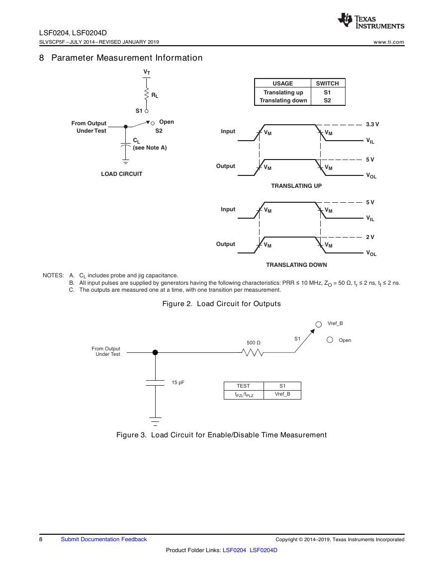
8 Parameter Measurement Information
www.ti.com
Figure 2. Load Circuit for Outputs
Figure 3. Load Circuit for Enable/Disable Time Measurement
8
Submit Documentation Feedback
Copyright © 2014–2019, Texas Instruments Incorporated
Product Folder Links: LSF0204 LSF0204D
From OutputUnderTest500ΩS1Vref_BOpen15 pFTESTS1t/tPZLPLZVref_BNOTES:A.CLincludes probe and jig capacitance.B.All input pulses are supplied by generators having the following characteristics:PRR≤≤≤10 MHz, Z= 50t2 ns, tOrfΩ,2 ns.C.The outputs are measured one at a time, with one transition per measurement.From OutputUnderTestCL(see Note A)LOAD CIRCUITTRANSLATING UPTRANSLATING DOWNRLTranslating upTranslating downS1S2USAGESWITCHVMVM3.3VVILInputVMVM5VVOLOutputVMVM5VVILInputVMVM2VVOLOutputVTS1S2Open�


 V2版本原理图(Capacitive-Fingerprint-Reader-Schematic_V2).pdf
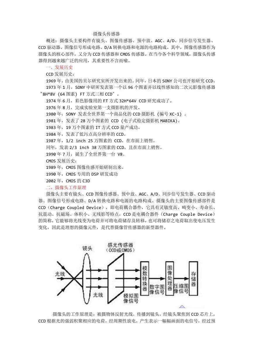 摄像头工作原理.doc
 VL53L0X简要说明(En.FLVL53L00216).pdf
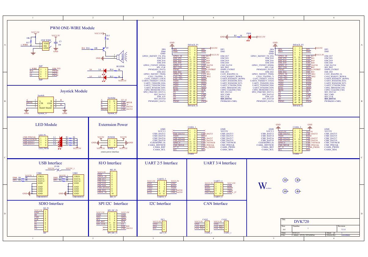 原理图(DVK720-Schematic).pdf
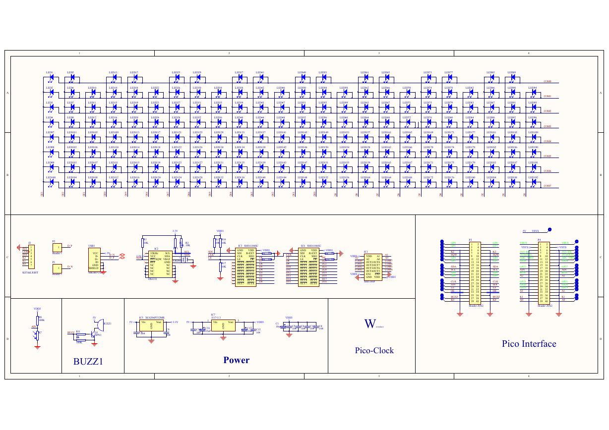 原理图(Pico-Clock-Green-Schdoc).pdf
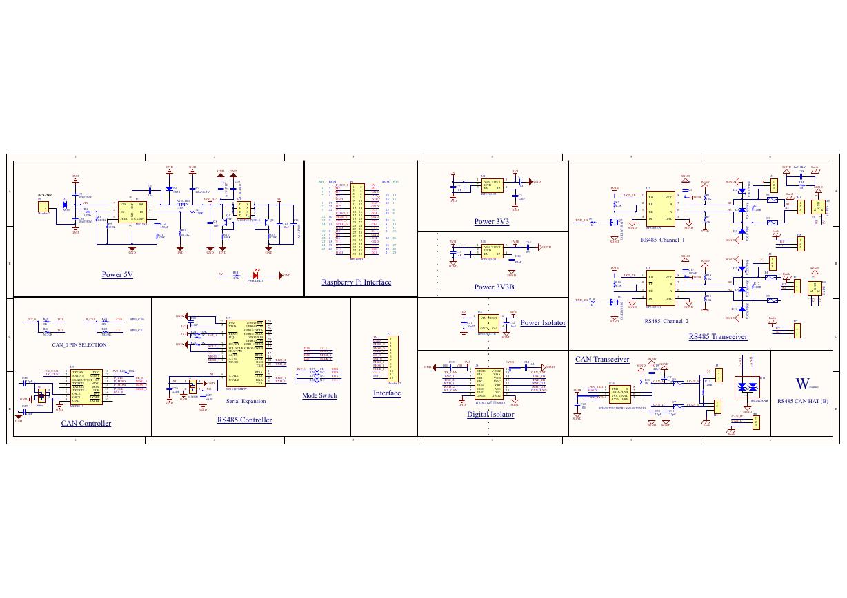 原理图(RS485-CAN-HAT-B-schematic).pdf
 File:SIM7500_SIM7600_SIM7800 Series_SSL_Application Note_V2.00.pdf
 ADS1263(Ads1262).pdf
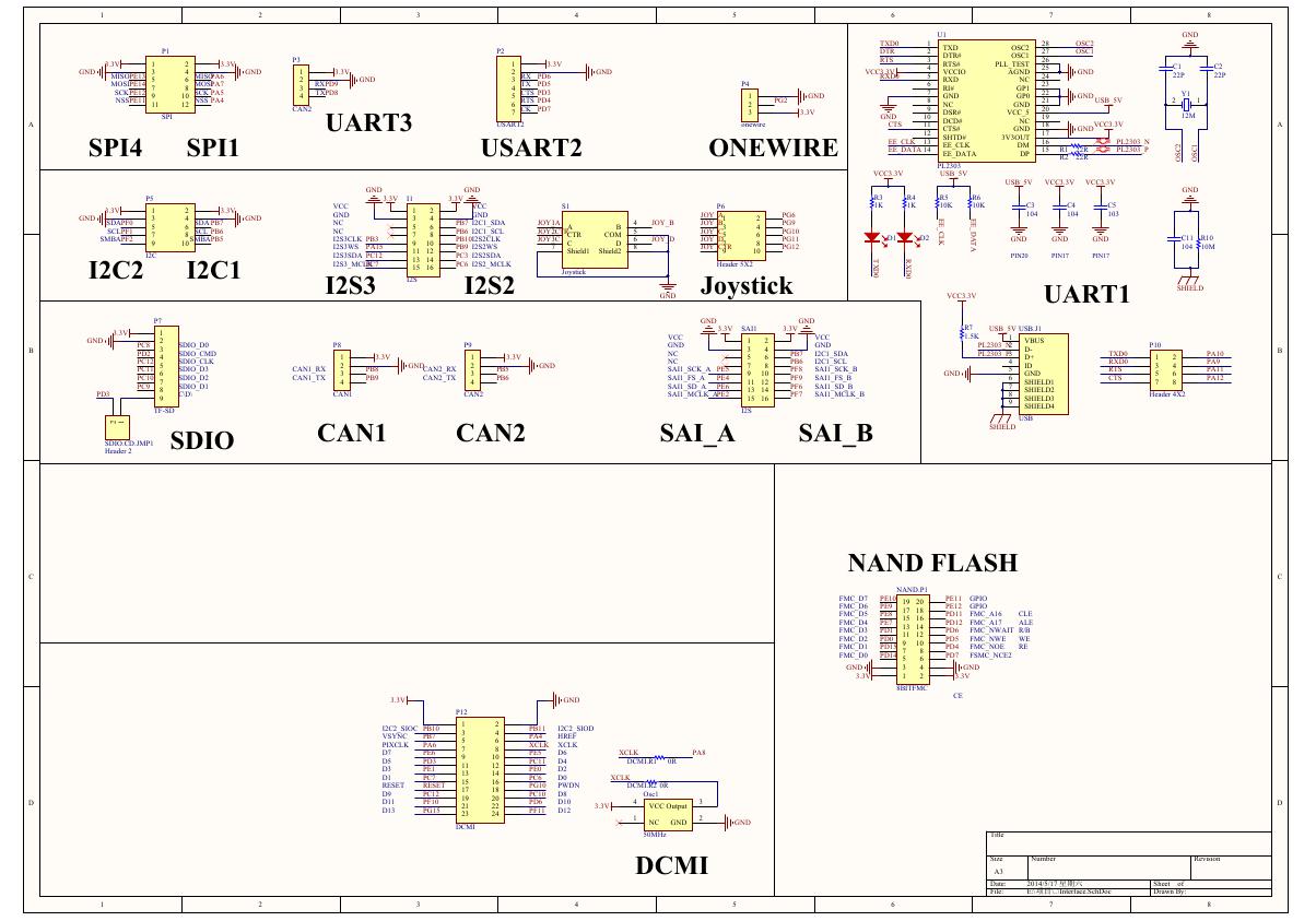 原理图(Open429Z-D-Schematic).pdf
 用户手册(Capacitive_Fingerprint_Reader_User_Manual_CN).pdf
 CY7C68013A(英文版)(CY7C68013A).pdf
 TechnicalReference_Dem.pdf