D Featuring Unitrode L293 and L293D
Products Now From Texas Instruments
D Wide Supply-Voltage Range: 4.5 V to 36 V
D Separate Input-Logic Supply
D Internal ESD Protection
D Thermal Shutdown
D High-Noise-Immunity Inputs
D Functionally Similar to SGS L293 and
SGS L293D
D Output Current 1 A Per Channel
(600 mA for L293D)
D Peak Output Current 2 A Per Channel
(1.2 A for L293D)
D Output Clamp Diodes for Inductive
Transient Suppression (L293D)
description/ordering information
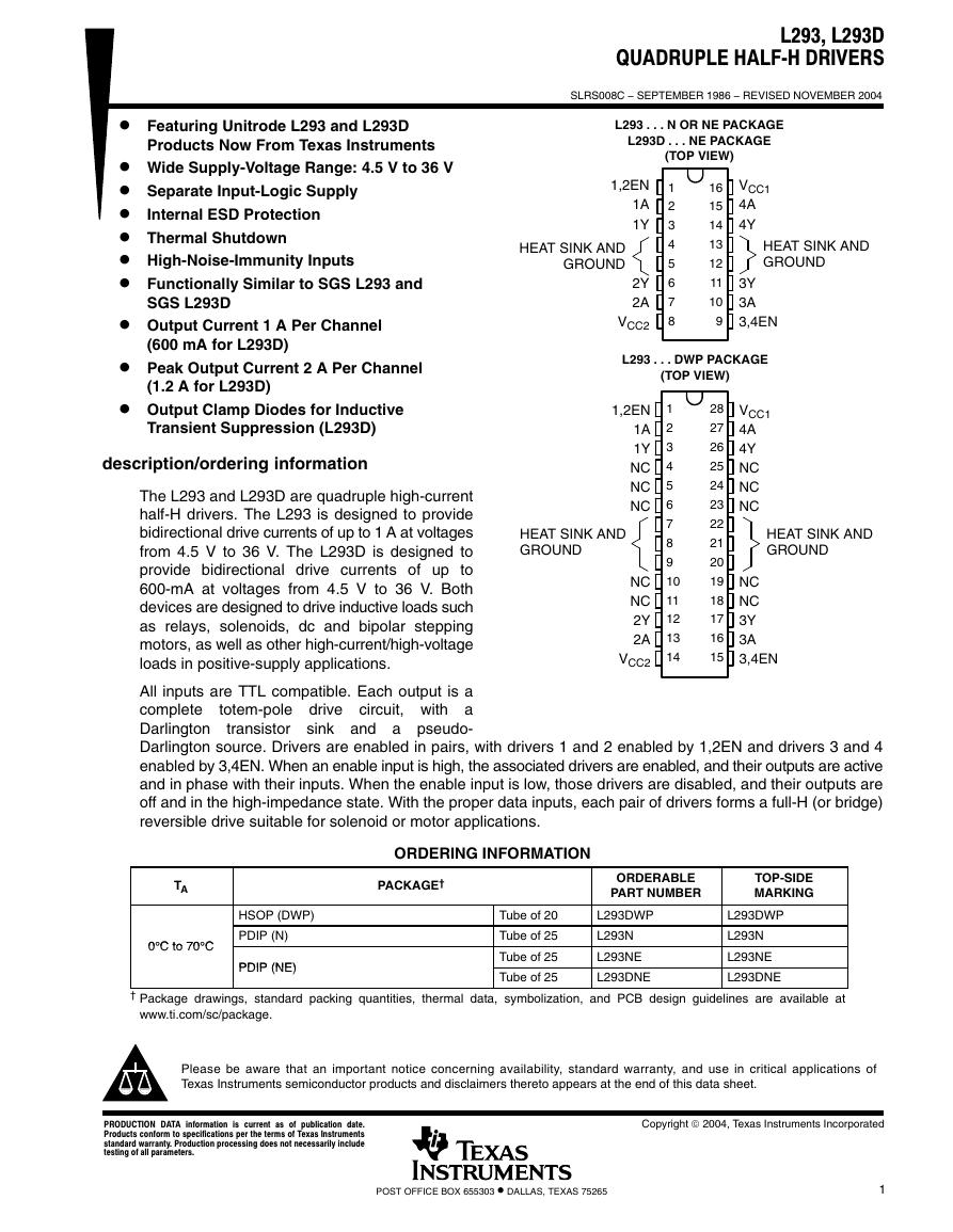
The L293 and L293D are quadruple high-current
half-H drivers. The L293 is designed to provide
bidirectional drive currents of up to 1 A at voltages
from 4.5 V to 36 V. The L293D is designed to
provide bidirectional drive currents of up to
600-mA at voltages from 4.5 V to 36 V. Both
devices are designed to drive inductive loads such
as relays, solenoids, dc and bipolar stepping
motors, as well as other high-current/high-voltage
loads in positive-supply applications.
L293, L293D
QUADRUPLE HALF-H DRIVERS
SLRS008C − SEPTEMBER 1986 − REVISED NOVEMBER 2004
L293 . . . N OR NE PACKAGE
L293D . . . NE PACKAGE
(TOP VIEW)
1,2EN
1A
1Y
HEAT SINK AND
GROUND
2Y
2A
VCC2
1
2
3
4
5
6
7
8
16
15
14
13
12
11
10
9
VCC1
4A
4Y
HEAT SINK AND
GROUND
3Y
3A
3,4EN
L293 . . . DWP PACKAGE
(TOP VIEW)
1,2EN
1A
1Y
NC
NC
NC
HEAT SINK AND
GROUND
NC
NC
2Y
2A
VCC2
1
2
3
4
5
6
7
8
9
10
11
12
13
14
28
27
26
25
24
23
22
21
20
19
18
17
16
15
VCC1
4A
4Y
NC
NC
NC
HEAT SINK AND
GROUND
NC
NC
3Y
3A
3,4EN
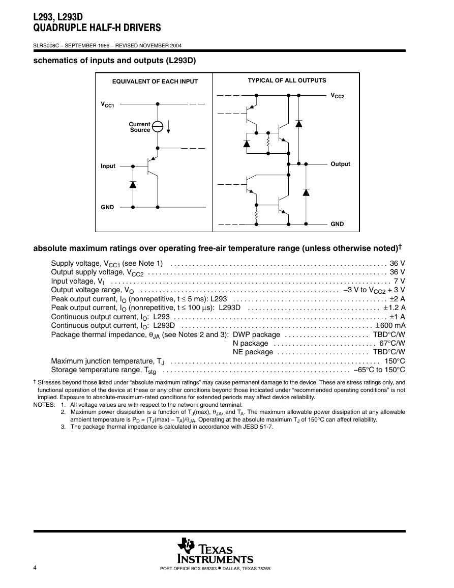
All inputs are TTL compatible. Each output is a
totem-pole drive circuit, with a
complete
Darlington
transistor sink and a pseudo-
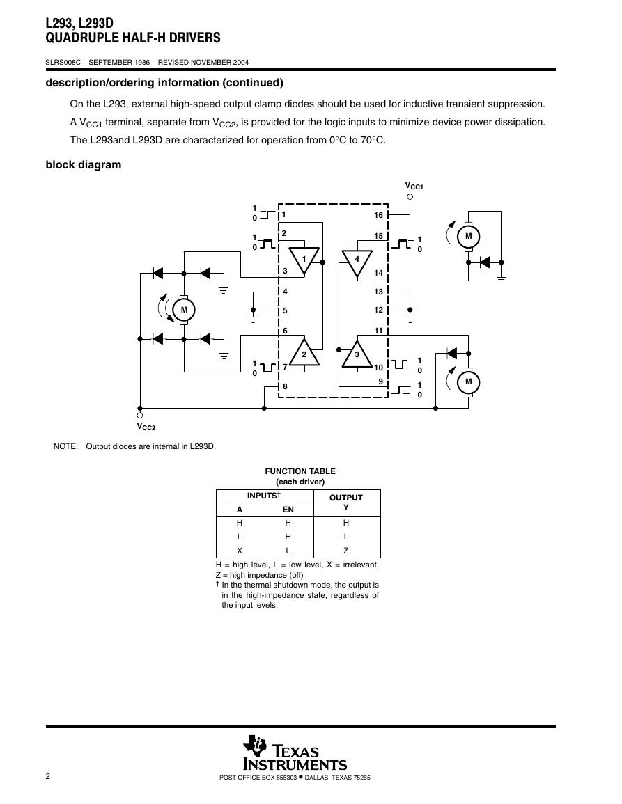
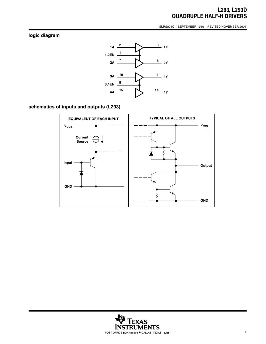
Darlington source. Drivers are enabled in pairs, with drivers 1 and 2 enabled by 1,2EN and drivers 3 and 4
enabled by 3,4EN. When an enable input is high, the associated drivers are enabled, and their outputs are active
and in phase with their inputs. When the enable input is low, those drivers are disabled, and their outputs are
off and in the high-impedance state. With the proper data inputs, each pair of drivers forms a full-H (or bridge)
reversible drive suitable for solenoid or motor applications.
TA
0°C to 70°C
0°C to 70°C
HSOP (DWP)
PDIP (N)
PDIP (NE)
PDIP (NE)
ORDERING INFORMATION
PACKAGE†
ORDERABLE
PART NUMBER
TOP-SIDE
MARKING
Tube of 20
Tube of 25
Tube of 25
Tube of 25
L293DWP
L293N
L293NE
L293DNE
L293DWP
L293N
L293NE
L293DNE
† Package drawings, standard packing quantities, thermal data, symbolization, and PCB design guidelines are available at
www.ti.com/sc/package.
Please be aware that an important notice concerning availability, standard warranty, and use in critical applications of
Texas Instruments semiconductor products and disclaimers thereto appears at the end of this data sheet.
PRODUCTION DATA information is current as of publication date.
Products conform to specifications per the terms of Texas Instruments
standard warranty. Production processing does not necessarily include
testing of all parameters.
Copyright 2004, Texas Instruments Incorporated
POST OFFICE BOX 655303 • DALLAS, TEXAS 75265
1
�
L293, L293D
QUADRUPLE HALF-H DRIVERS
SLRS008C − SEPTEMBER 1986 − REVISED NOVEMBER 2004
description/ordering information (continued)
On the L293, external high-speed output clamp diodes should be used for inductive transient suppression.
A VCC1 terminal, separate from VCC2, is provided for the logic inputs to minimize device power dissipation.
The L293and L293D are characterized for operation from 0°C to 70°C.
block diagram
1
0
1
0
1
0
1
2
3
4
5
6
7
8
1
2
VCC1
1
0
1
0
1
0
16
15
14
13
12
11
10
9
4
3
M
M
M
VCC2
NOTE:
Output diodes are internal in L293D.
FUNCTION TABLE
(each driver)
INPUTS†
OUTPUT
OUTPUT
A
H
L
X
EN
H
H
L
Y
H
L
Z
H = high level, L = low level, X = irrelevant,
Z = high impedance (off)
† In the thermal shutdown mode, the output is
in the high-impedance state, regardless of
the input levels.
2
POST OFFICE BOX 655303 • DALLAS, TEXAS 75265
�
logic diagram
L293, L293D
QUADRUPLE HALF-H DRIVERS
SLRS008C − SEPTEMBER 1986 − REVISED NOVEMBER 2004
1A
1,2EN
2A
3A
3,4EN
4A
2
1
7
10
9
15
ÁÁ
ÁÁ
ÁÁ
ÁÁ
ÁÁ
ÁÁ
ÁÁ
ÁÁ
ÁÁ
ÁÁ
3
6
11
14
1Y
2Y
3Y
4Y
schematics of inputs and outputs (L293)
EQUIVALENT OF EACH INPUT
TYPICAL OF ALL OUTPUTS
Current
Source
VCC1
Input
GND
VCC2
Output
GND
POST OFFICE BOX 655303 • DALLAS, TEXAS 75265
3
�
L293, L293D
QUADRUPLE HALF-H DRIVERS
SLRS008C − SEPTEMBER 1986 − REVISED NOVEMBER 2004
schematics of inputs and outputs (L293D)
EQUIVALENT OF EACH INPUT
TYPICAL OF ALL OUTPUTS
Current
Source
VCC1
Input
GND
VCC2
Output
GND
absolute maximum ratings over operating free-air temperature range (unless otherwise noted)†
. . . . . . . . . . . . . . . . . . . . . . . . . . . . . . . . . . . . . . . . . . . . . . . . . . . . . .
. . . . . . . . . . . . . . . . . . . . . . . . . . . . . . . . . . . . . . . . . . . . . . . . . . . . . . . . . . .
. . . . . . . . . . . . . . . . . . . . . . . . . . . . . . . . . . . . . . . . . . . . . . . . . . . . . . . . . . . . . . . . .
. . . . . . . . . . . . . . . . . . . . . . . . . . . . . . . . . . . . . . . . . . . . . . . . . . . . . . . . . . . . . . . . . . . . . . . . . . . .
Supply voltage, VCC1 (see Note 1)
Output supply voltage, VCC2
Input voltage, VI
Output voltage range, VO
Peak output current, IO (nonrepetitive, t ≤ 5 ms): L293
Peak output current, IO (nonrepetitive, t ≤ 100 µs): L293D
Continuous output current, IO: L293
Continuous output current, IO: L293D
Package thermal impedance, θJA (see Notes 2 and 3): DWP package
36 V
36 V
7 V
−3 V to VCC2 + 3 V
±2 A
±1.2 A
±1 A
±600 mA
TBD°C/W
67°C/W
TBD°C/W
150°C
−65°C to 150°C
† Stresses beyond those listed under “absolute maximum ratings” may cause permanent damage to the device. These are stress ratings only, and
functional operation of the device at these or any other conditions beyond those indicated under “recommended operating conditions” is not
implied. Exposure to absolute-maximum-rated conditions for extended periods may affect device reliability.
. . . . . . . . . . . . . . . . . . . . . . . . . . . . . . . . . . . . . . . . . . . . . . . . . . . .
. . . . . . . . . . . . . . . . . . . . . . .
N package
NE package
. . . . . . . . . . . . . . . . . . . . . . . . . . . .
. . . . . . . . . . . . . . . . . . . . . . . . .
. . . . . . . . . . . . . . . . . . . . . . . . . . . . . . . . . . . . . . . . . .
. . . . . . . . . . . . . . . . . . . . . . . . . . . . . . . . . . . .
. . . . . . . . . . . . . . . . . . . . . . . . . . . . . . . . . . . . . . . . . . . . . . . . . . . . . . . . . .
Maximum junction temperature, TJ
Storage temperature range, Tstg
. . . . . . . . . . . . . . . . . . . . . . . . . . . . . . . . . . . . . . . . . . . . . . . . . . . . . . . . .
. . . . . . . . . . . . . . . . . . . . . . . . . . . . . . . . . . . . . . . . . . . . . . . . . . .
NOTES: 1. All voltage values are with respect to the network ground terminal.
2. Maximum power dissipation is a function of TJ(max), qJA, and TA. The maximum allowable power dissipation at any allowable
ambient temperature is PD = (TJ(max) − TA)/qJA. Operating at the absolute maximum TJ of 150°C can affect reliability.
3. The package thermal impedance is calculated in accordance with JESD 51-7.
4
POST OFFICE BOX 655303 • DALLAS, TEXAS 75265
�
L293, L293D
QUADRUPLE HALF-H DRIVERS
SLRS008C − SEPTEMBER 1986 − REVISED NOVEMBER 2004
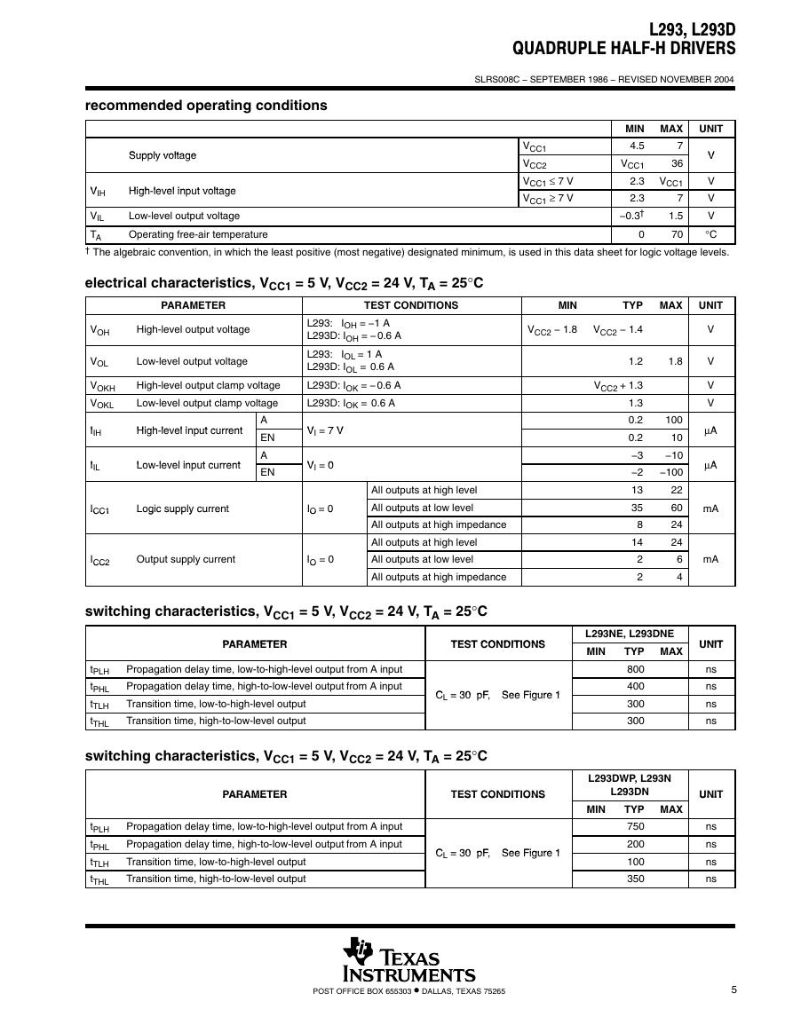
recommended operating conditions
Supply voltage
Supply voltage
V
VIH
High level input voltage
High-level input voltage
VCC1
VCC2
VCC1 ≤ 7 V
VCC1 ≥ 7 V
MIN MAX
7
4.5
VCC1
36
VCC1
2.3
7
2.3
−0.3†
1.5
Low-level output voltage
Operating free-air temperature
VIL
TA
† The algebraic convention, in which the least positive (most negative) designated minimum, is used in this data sheet for logic voltage levels.
electrical characteristics, VCC1 = 5 V, VCC2 = 24 V, TA = 25°C
0
70
PARAMETER
TEST CONDITIONS
MIN
TYP MAX
UNIT
VCC2 − 1.8
VCC2 − 1.4
UNIT
V
V
V
V
V
°C
V
V
V
V
µA
A
µA
A
mA
mA
mA
UNIT
UNIT
ns
ns
ns
ns
UNIT
UNIT
ns
ns
ns
ns
VOH
VOL
VOKH
VOKL
I
IIH
I
IIL
High-level output voltage
Low-level output voltage
High-level output clamp voltage
Low-level output clamp voltage
High level input current
High-level input current
Low level input current
Low-level input current
A
EN
A
EN
ICC1
ICC1
Logic supply current
Logic supply current
ICC2
CC2
Output supply current
pp y
p
L293: IOH = −1 A
L293D: IOH = − 0.6 A
L293: IOL = 1 A
L293D: IOL = 0.6 A
L293D: IOK = − 0.6 A
L293D: IOK = 0.6 A
V
7 V
VI = 7 V
V
0
VI = 0
IO = 0
IO
0
IO = 0
O
All outputs at high level
All outputs at low level
All outputs at high impedance
All outputs at high level
All outputs at low level
All outputs at high impedance
switching characteristics, VCC1 = 5 V, VCC2 = 24 V, TA = 25°C
PARAMETER
PARAMETER
TEST CONDITIONS
TEST CONDITIONS
tPLH
tPHL
tTLH
tTHL
Propagation delay time, low-to-high-level output from A input
Propagation delay time, high-to-low-level output from A input
Transition time, low-to-high-level output
Transition time, high-to-low-level output
CL = 30 pF, See Figure 1
C = 30 pF See Figure 1
switching characteristics, VCC1 = 5 V, VCC2 = 24 V, TA = 25°C
PARAMETER
PARAMETER
TEST CONDITIONS
TEST CONDITIONS
tPLH
tPHL
tTLH
tTHL
Propagation delay time, low-to-high-level output from A input
Propagation delay time, high-to-low-level output from A input
Transition time, low-to-high-level output
Transition time, high-to-low-level output
C = 30 pF See Figure 1
CL = 30 pF, See Figure 1
1.2
1.8
VCC2 + 1.3
1.3
0.2
0.2
−3
−2
13
35
8
14
2
2
100
10
−10
−100
22
60
24
24
6
4
L293NE, L293DNE
MIN
TYP MAX
800
400
300
300
L293DWP, L293N
L293DN
MIN
TYP MAX
750
200
100
350
POST OFFICE BOX 655303 • DALLAS, TEXAS 75265
5
�
L293, L293D
QUADRUPLE HALF-H DRIVERS
SLRS008C − SEPTEMBER 1986 − REVISED NOVEMBER 2004
PARAMETER MEASUREMENT INFORMATION
Input
5 V 24 V
VCC2
VCC1
A
Pulse
Generator
(see Note B)
3 V
EN
tf
90%
Input
50%
tr
90%
50%
10%
10%
tw
Y
Output
CL = 30 pF
(see Note A)
Output
tPHL
90%
tTHL
50%
50%
10%
10%
3 V
0
tPLH
VOH
90%
VOL
tTLH
TEST CIRCUIT
VOLTAGE WAVEFORMS
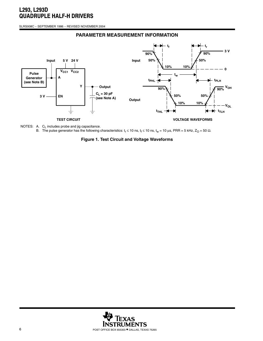
NOTES: A. CL includes probe and jig capacitance.
B. The pulse generator has the following characteristics: tr ≤ 10 ns, tf ≤ 10 ns, tw = 10 µs, PRR = 5 kHz, ZO = 50 Ω.
Figure 1. Test Circuit and Voltage Waveforms
6
POST OFFICE BOX 655303 • DALLAS, TEXAS 75265
�
Control A
Control B
10 kΩ
1,2EN
1
1A
2
2A
7
3,4EN
9
3A
10
4A
15
L293, L293D
QUADRUPLE HALF-H DRIVERS
SLRS008C − SEPTEMBER 1986 − REVISED NOVEMBER 2004
APPLICATION INFORMATION
5 V
VCC1
16
24 V
VCC2
8
Motor
1Y
3
2Y
6
3Y
11
4Y
14
Thermal
Shutdown
4, 5, 12, 13
GND
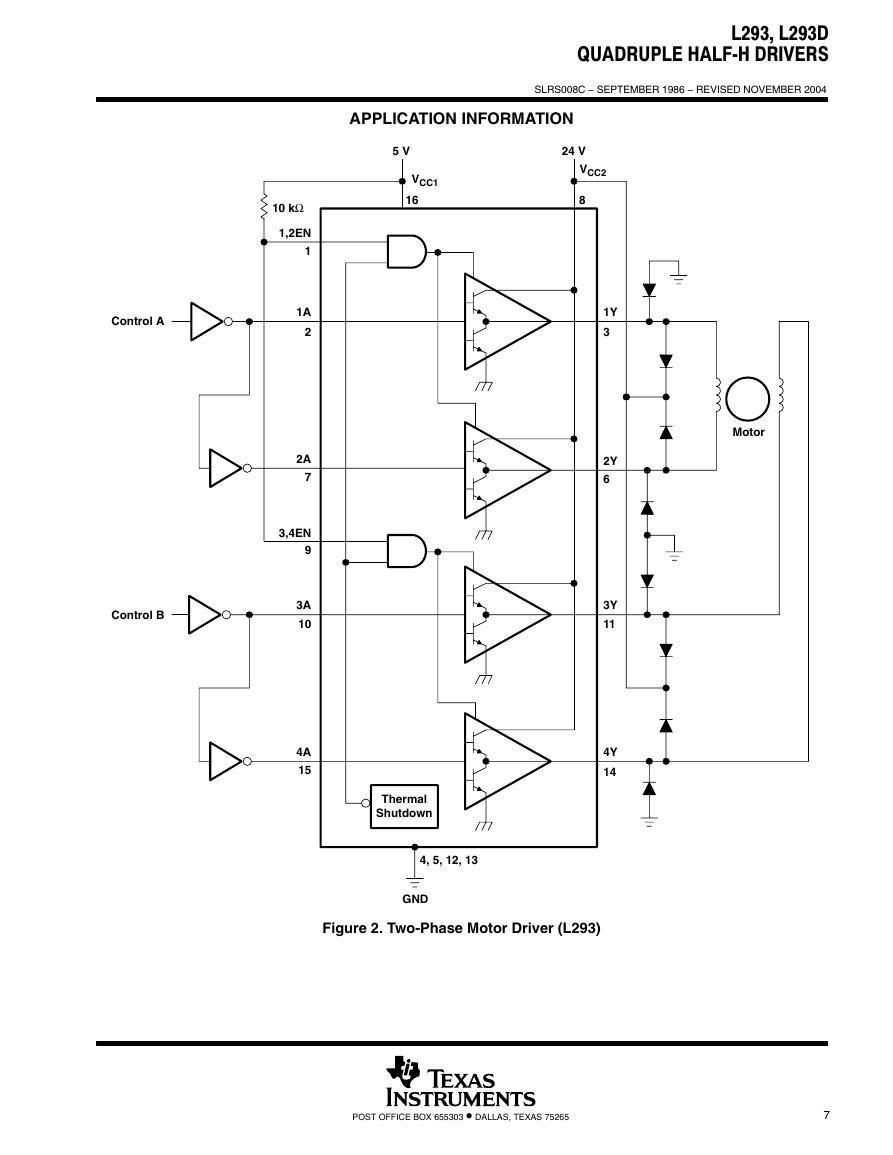
Figure 2. Two-Phase Motor Driver (L293)
POST OFFICE BOX 655303 • DALLAS, TEXAS 75265
7
�
L293, L293D
QUADRUPLE HALF-H DRIVERS
SLRS008C − SEPTEMBER 1986 − REVISED NOVEMBER 2004
APPLICATION INFORMATION
5 V
24 V
VCC1
16
VCC2
8
Control A
Control B
10 kΩ
1,2EN
1
1A
2
2A
7
3,4EN
9
3A
10
4A
15
Motor
1Y
3
2Y
6
3Y
11
4Y
14
Thermal
Shutdown
4, 5, 12, 13
GND
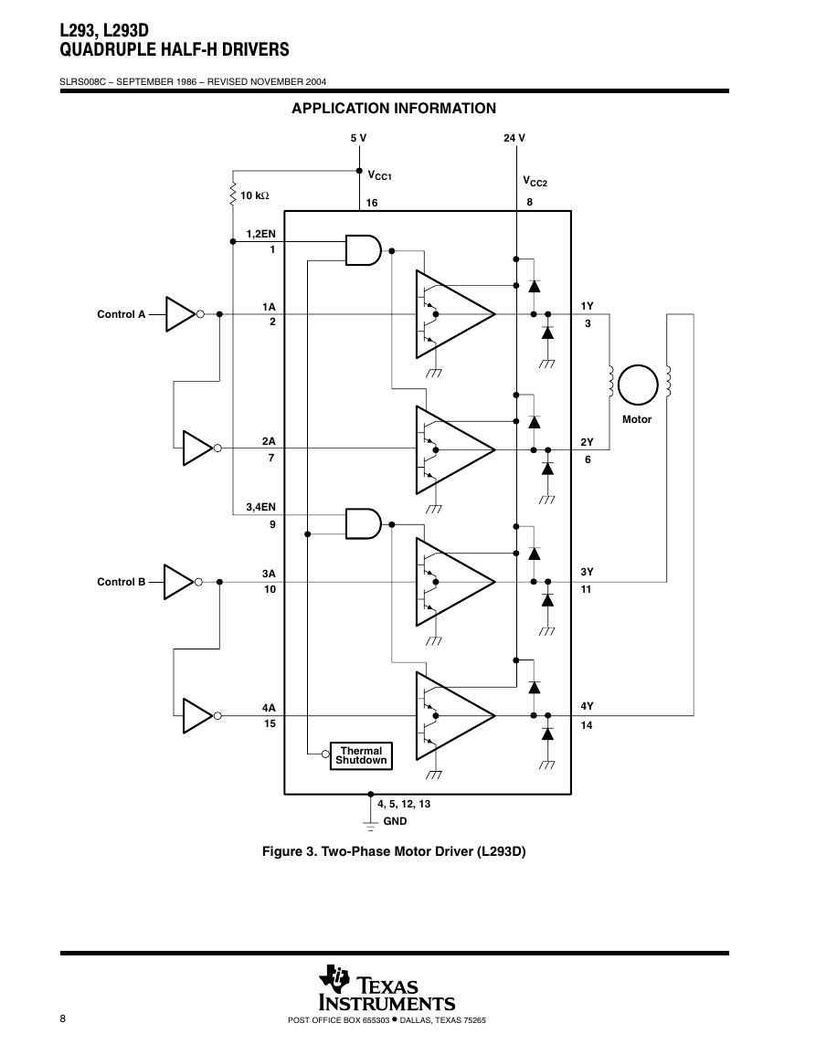
Figure 3. Two-Phase Motor Driver (L293D)
8
POST OFFICE BOX 655303 • DALLAS, TEXAS 75265
�


 V2版本原理图(Capacitive-Fingerprint-Reader-Schematic_V2).pdf
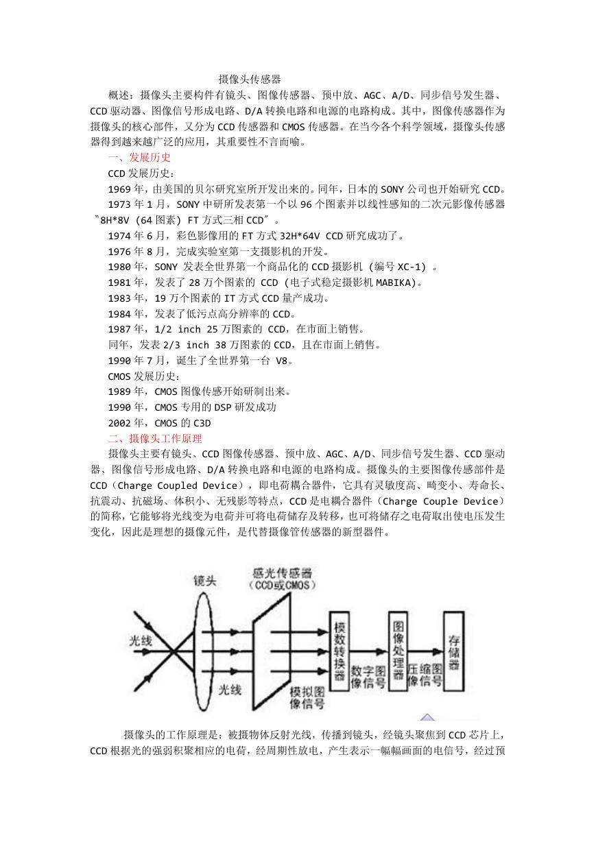 摄像头工作原理.doc
 VL53L0X简要说明(En.FLVL53L00216).pdf
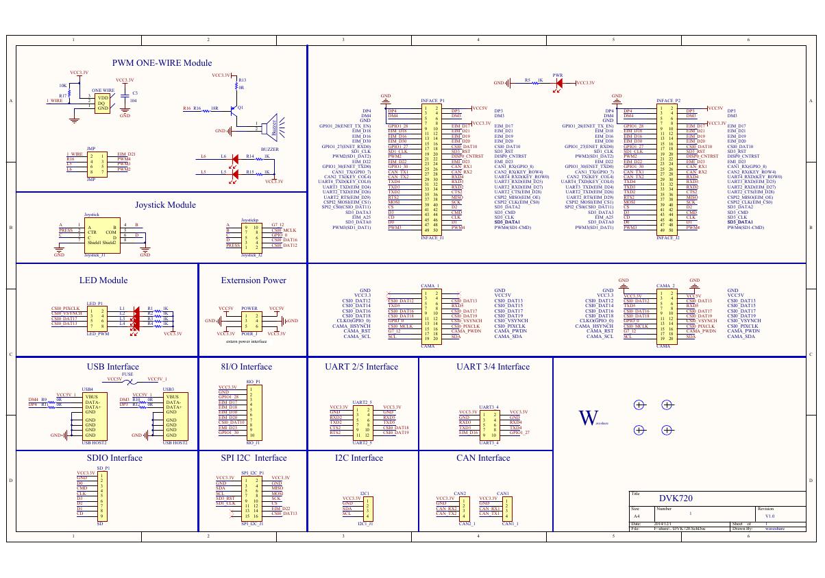 原理图(DVK720-Schematic).pdf
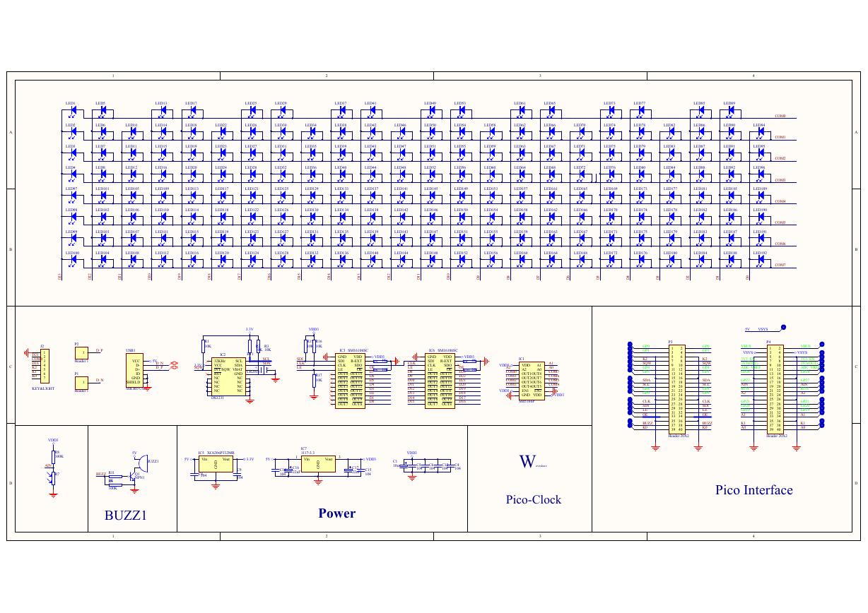 原理图(Pico-Clock-Green-Schdoc).pdf
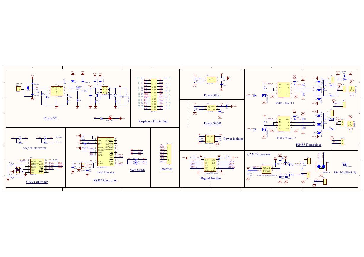 原理图(RS485-CAN-HAT-B-schematic).pdf
 File:SIM7500_SIM7600_SIM7800 Series_SSL_Application Note_V2.00.pdf
 ADS1263(Ads1262).pdf
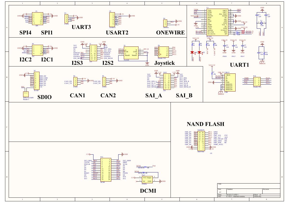 原理图(Open429Z-D-Schematic).pdf
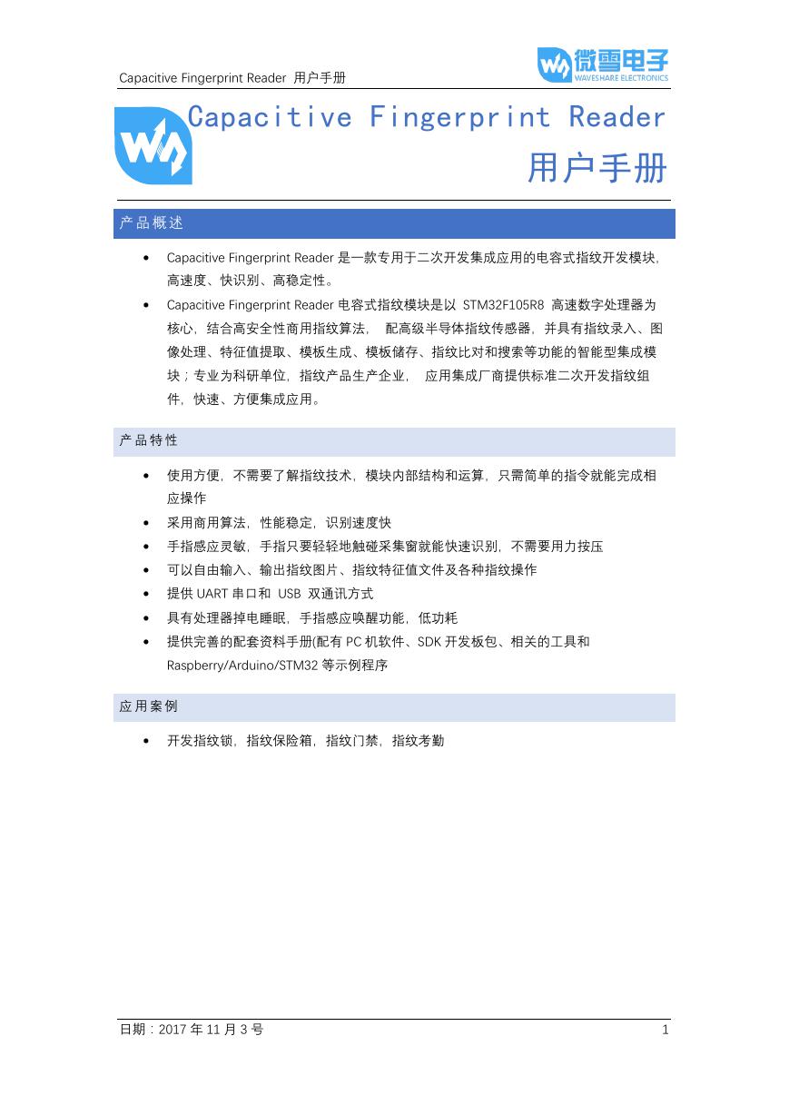 用户手册(Capacitive_Fingerprint_Reader_User_Manual_CN).pdf
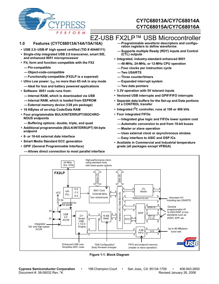 CY7C68013A(英文版)(CY7C68013A).pdf
 TechnicalReference_Dem.pdf