ETA6003
2.5A, 3MHz Switching Charger with Dynamic Power Path Management
DESCRIPTION
ETA6003 is a switching Li-Ion battery charger with dynamic power-path control and input current limiting. When a battery is connected,
depending on the battery voltage, the DC-DC switching regulator either pre-conditions, fast-charges the battery or just regulates a system
voltage (VSYS) to a preset voltage. It does not require an external sense resistor for current sensing. The charging current is determined by
programming ISET1 or ISET2 pin, depending on the state of the USB_DET. If USB_DET is low, indicating a valid AC adapter input is present, the
charge current is set by ISET1; otherwise, it is set by ISET2. When the battery voltage reaches the termination voltage i.e. 4.2V, the charging
path disconnects SYS to BATT. The ETA6003 also includes a dynamic power path when the SYS load current exceeds current limit of the DCDC
regulator internally set, the SYS voltage falls below VBATT, ETA6003 turns on the power-path to supplement the system load through the battery.
FEATURES
Switching Charger with Power Path Management
Up to 95% DC-DC Efficiency
50mΩ Power Path MOSFET
Up to 2.5A Max charging current
Instant on with a dead Battery or no Battery
No battery detection
No External Sense resistor
Programmable USB and AC IN Charging Current
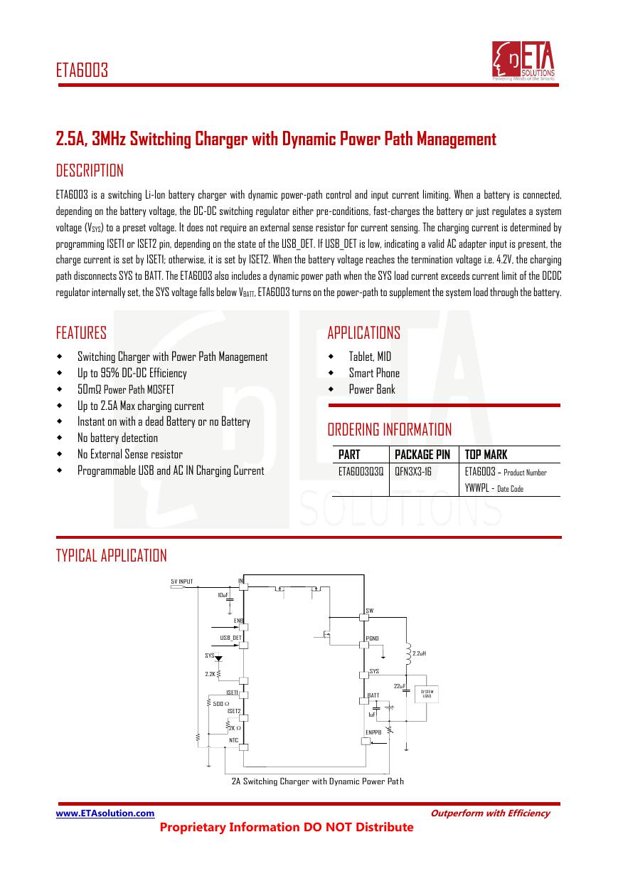
TYPICAL APPLICATION
APPLICATIONS
Tablet, MID
Smart Phone
Power Bank
ORDERING INFORMATION
PART
ETA6003Q3Q QFN3X3-16
PACKAGE PIN
TOP MARK
ETA6003 - Product Number
YWWPL - Date Code
www.ETAsolution.com Outperform with Efficiency
Proprietary Information DO NOT Distribute
SYSSWPGNDINBATTNTCISET1ISET2USB_DETENBSYSSYSTEM LOAD2.2uH2.2K2KΩ 500Ω 5V INPUT22uF10uF1uFENPPB2A Switching Charger with Dynamic Power Path�
ETA6003
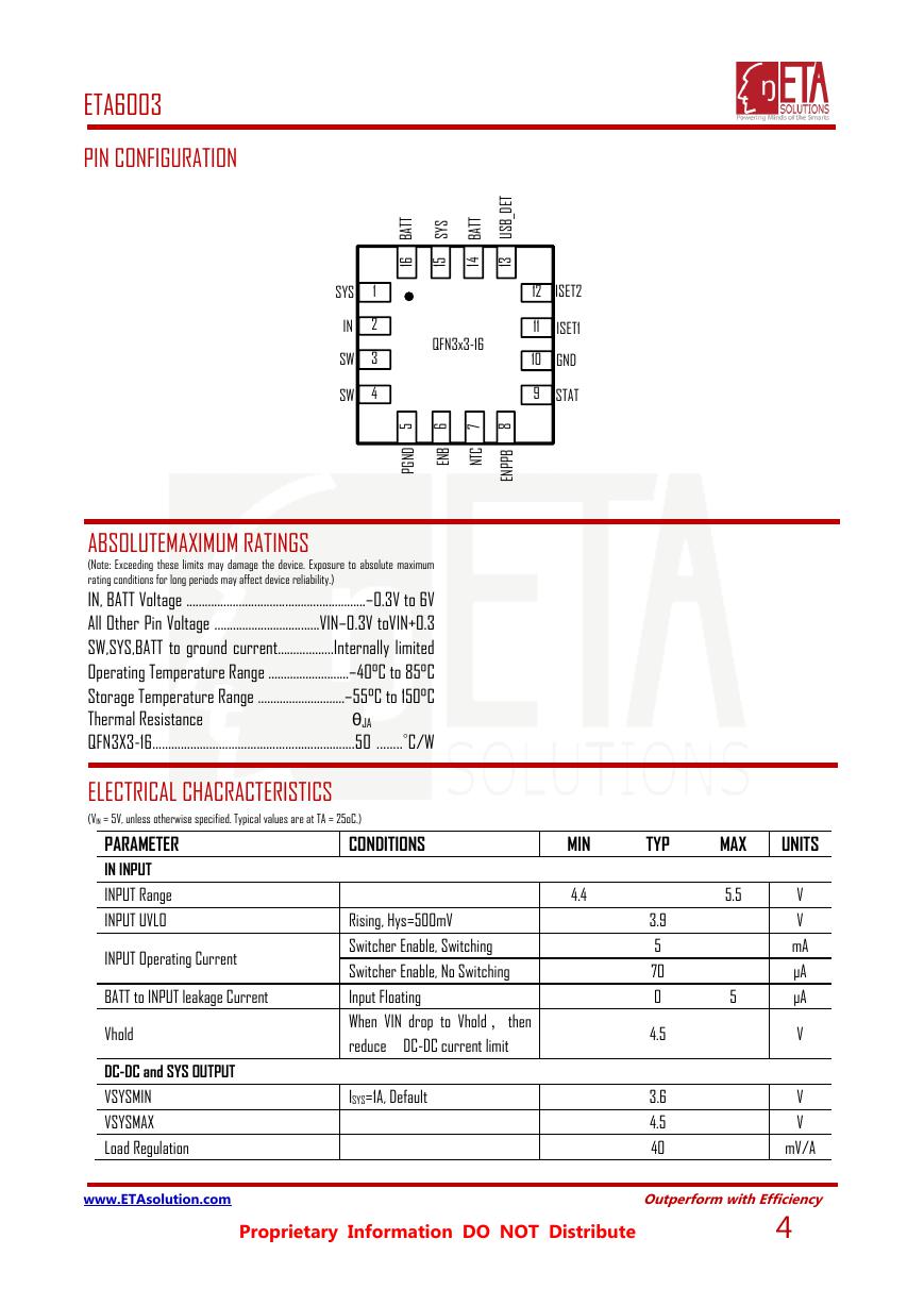
PIN CONFIGURATION
ABSOLUTEMAXIMUM RATINGS
(Note: Exceeding these limits may damage the device. Exposure to absolute maximum
rating conditions for long periods may affect device reliability.)
IN, BATT Voltage ..........................................................–0.3V to 6V
All Other Pin Voltage ..................................VIN–0.3V toVIN+0.3
SW,SYS,BATT to ground current……………...Internally limited
Operating Temperature Range ……………….....…–40°C to 85°C
Storage Temperature Range ……………………….–55°C to 150°C
Thermal Resistance θJA
QFN3X3-16……………………………………………………….50 ........C/W
ELECTRICAL CHACRACTERISTICS
(VIN = 5V, unless otherwise specified. Typical values are at TA = 25oC.)
PARAMETER
IN INPUT
INPUT Range
INPUT UVLO
INPUT Operating Current
BATT to INPUT leakage Current
Vhold
DC-DC and SYS OUTPUT
VSYSMIN
VSYSMAX
Load Regulation
CONDITIONS
MIN
TYP
MAX
UNITS
4.4
Rising, Hys=500mV
Switcher Enable, Switching
Switcher Enable, No Switching
Input Floating
When VIN drop to Vhold , then
reduce DC-DC current limit
ISYS=1A, Default
3.9
5
70
0
4.5
3.6
4.5
40
5.5
5
V
V
mA
μA
μA
V
V
V
mV/A
www.ETAsolution.com Outperform with Efficiency
Proprietary Information DO NOT Distribute 4
12QFN3x3-16INSYS35SW67PGND11109STATGND16BATT1514BATT4SW812ISET213USB_DETNTCENPPBISET1ENBSYS�
ETA6003
PARAMETER
Line Regulation
Switching Frequency
Max duty
HIGHSIDE MOS RDSON
LOWSIDE MOS RDSON
HIGHSIDE Current limit
SYS UVLO
Thermal Shutdown
POWER PATH Management
BATT TO SYS RDSON
BATTERY CHARGER
Battery CV voltage
CONDITIONS
VIN =4.75 to 5.25V
ISW =500mA
ISW =500mA
Falling, Hys=200mV
Rising, Hys=30oC
MIN
100
IBAT =0mA, default
4.16
Charger Restart Threshold
From DONE to FastCharge
Battery Pre-condition Voltage
VBAT Rising Hys=180mV
Pre-Condition Charge Current
1.6
RISET1 =500Ω, USB_DET= low
Icharge=1V*1000/RISET1
RISET2 =2KΩ, USB_DET= high
Icharge=1V*1000/RISET2
Percent of the fast charge current
Charger Suspended
Charger Suspended
ISTATS=10mA
TYP
0.04
3
100
60
3.5
2.25
160
50
4.2
-150
2.9
100
2
0.5
120
960
10%
76.5
35
1.5
100
0
UNITS
%/V
MHz
%
mΩ
mΩ
A
V
oC
mΩ
V
mV
V
mA
A
A
min
min
%VIN
%VIN
%VIN
mV
μA
V
V
V
MAX
4.24
0.3
0.2
AC Fast Charge Current
USB Charge Current
Pre-condition Timer
Fast-Charge Timer
EOC current
THERMISTOR MONITOR
NTC Threshold, Cold
NTC Threshold, Hot
NTC Threshold Hysteresis
NTC Disable Threshold
NTC Input Leakage
LOGIC INPUT, STATS
ENB, ENPPB Logic Input High
ENB, ENPPB Logic Input Low
STAT Output Low Voltage
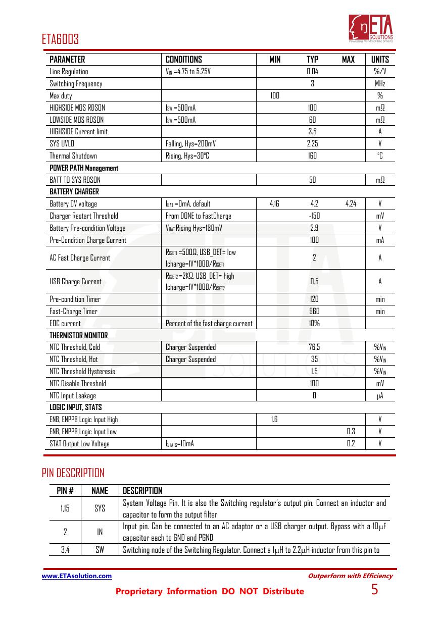
PIN DESCRIPTION
PIN #
NAME
1,15
2
3,4
SYS
IN
SW
DESCRIPTION
System Voltage Pin. It is also the Switching regulator’s output pin. Connect an inductor and
capacitor to form the output filter
Input pin. Can be connected to an AC adaptor or a USB charger output. Bypass with a 10F
capacitor each to GND and PGND
Switching node of the Switching Regulator. Connect a 1H to 2.2H inductor from this pin to
www.ETAsolution.com Outperform with Efficiency
Proprietary Information DO NOT Distribute 5
�
ETA6003
PIN #
NAME
5
6
7
8
9
10
11
12
PGND
ENB
NTC
ENPPB
STATS
GND
ISET1
ISET2
13
USB_DET
14,16
BATT
DESCRIPTION
SYS
Power Ground. Bypass with a 10F capacitor to IN with a shortest possible trace
Active Low Enable pin. Tie this pin low to enable the Charging, tie high to disable Charging, while
still keeping powerpath from BATT to SYS
Thermistor input
Shipping mode enable Pin. Tie to GND to enable power path from BATT to SYS, tie to BATT, to
disable this path thereby enabling shipping mode to save power to extend battery life.
Status pin for Charging status indications. An open drain device capable of driving 10mA current
Analog Ground Pin. Bypass with a 10F capacitor to IN
AC Fast Charge Current set pin for AC input. Connecting a Resistor between ISET1 to GND This
sets the fast charge current value for AC adapter when USB_DET is low.
USB Charge Current set pin for USB input. Connecting a Resistor between ISET2 to GND This
sets the charge current value for USB input when USB_DET is high.
Charge current selecting input. Pull this pin low if an AC adapter is connected and select fast
charging current to be set by ISET1. And set this pin high if a USB input is connected and select
USB charging current to be set by ISET2. It is default low.
Battery pin. Connect a Battery to this pin
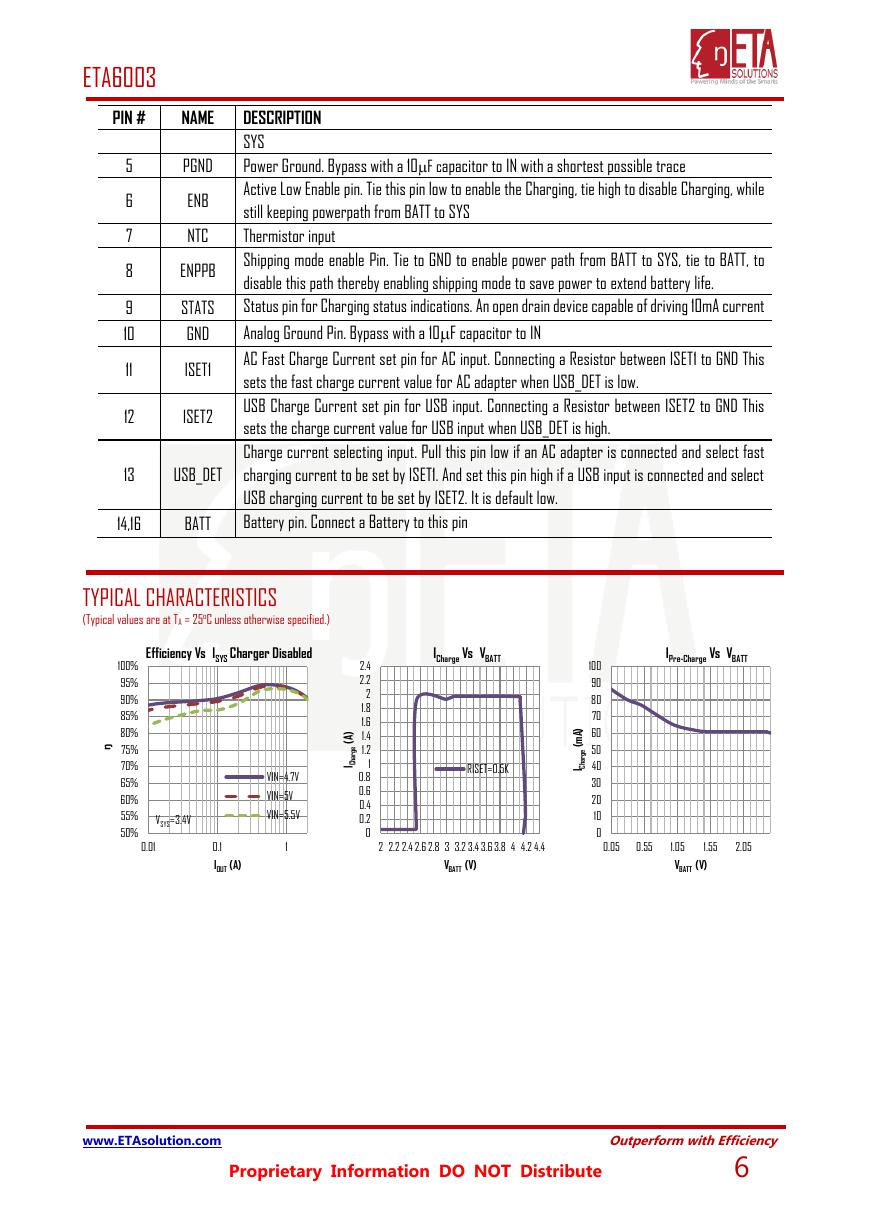
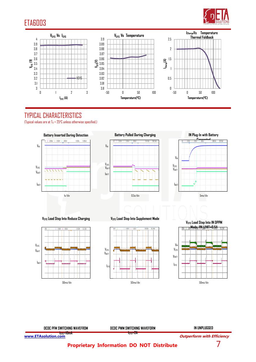
TYPICAL CHARACTERISTICS
(Typical values are at TA = 25oC unless otherwise specified.)
Efficiency Vs ISYS Charger Disabled
IPre-Charge Vs VBATT
ICharge Vs VBATT
RISET=0.5K
)
A
(
e
g
r
a
h
C
I
2.4
2.2
2
1.8
1.6
1.4
1.2
1
0.8
0.6
0.4
0.2
0
)
A
m
(
e
g
r
a
h
C
I
100
90
80
70
60
50
40
30
20
10
0
1
2 2.2 2.4 2.6 2.8 3 3.2 3.4 3.6 3.8 4 4.2 4.4
0.05
0.55
1.05
1.55
2.05
VBATT (V)
VBATT (V)
ŋ
100%
95%
90%
85%
80%
75%
70%
65%
60%
55%
50%
VIN=4.7V
VIN=5V
VIN=5.5V
VSYS=3.4V
0.01
0.1
IOUT (A)
www.ETAsolution.com Outperform with Efficiency
Proprietary Information DO NOT Distribute 6
�
ETA6003
VSYS Vs Temperature
)
V
(
S
Y
S
V
4
3.9
3.8
3.7
3.6
3.5
3.4
3.3
3.2
3.1
3
VSYS Vs ISYS
)
V
(
S
Y
S
V
3.9
3.89
3.88
3.87
3.86
3.85
3.84
3.83
3.82
3.81
3.8
VSYS
IChargeVs Temperature
Thermal Foldback
2.5
2
1.5
1
0.5
0
)
A
(
e
g
r
a
h
C
I
0
1
2
3
-50
0
50
100
-50
0
50
100
ISYS (A)
Temperature(OC)
Temperature(OC)
VIN
VSYS
VBATT
IBATT
VSYS
VBATT
IBATT
www.ETAsolution.com Outperform with Efficiency
ISYS=10mA
DCDC PFM SWITCHING WAVEFROM
DCDC PWM SWITCHING WAVEFORM
ISYS=2A
IN UNPLUGGED
Proprietary Information DO NOT Distribute 7
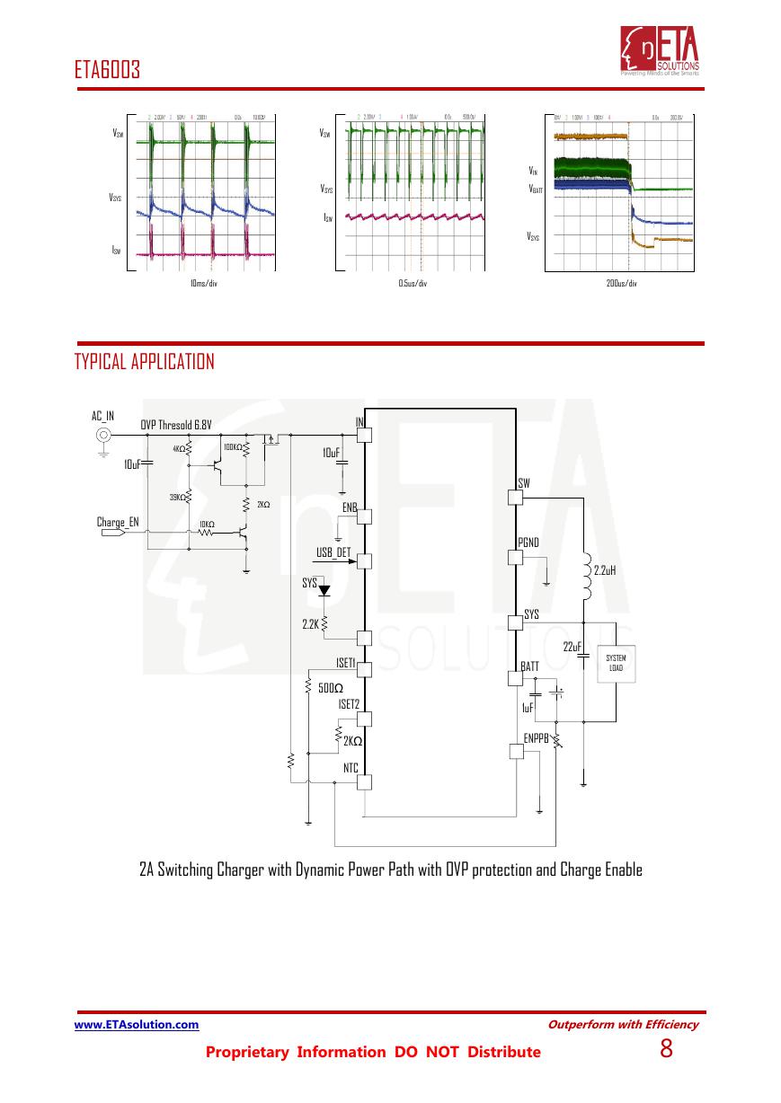
TYPICAL CHARACTERISTICS
(Typical values are at TA = 25oC unless otherwise specified.)
Battery Inserted During Detection
Battery Pulled During Charging
IN Plug-In with Battery
Connected
VIN
VSYS
VBATT
IBATT
VIN
VSYS
VBATT
IBATT
1s/div
0.5s/div
5ms/div
VSYS Load Step Into Reduce Charging
VSYS Load Step Into Supplement Mode
VSYS Load Step Into IN DPPM
Mode, IIN LIMIT=0.5A
VSYS
VBATT
ISYS
VIN
VSYS
VBATT
ISYS
50ms/div
50ms/div
50ms/div
�
ETA6003
VSW
VSYS
ISW
VIN
VBATT
VSYS
VSW
VSYS
ISW
10ms/div
0.5us/div
200us/div
TYPICAL APPLICATION
2A Switching Charger with Dynamic Power Path with OVP protection and Charge Enable
www.ETAsolution.com Outperform with Efficiency
Proprietary Information DO NOT Distribute 8
SYSSWPGNDINBATTNTCISET1ISET2USB_DETENBSYSSYSTEM LOAD2.2uH2.2K2KΩ 500Ω 22uF10uF1uFCharge_ENAC_IN2KΩ 4KΩ 39KΩ OVP Thresold 6.8V10uF10KΩ 100KΩ ENPPB�
ETA6003
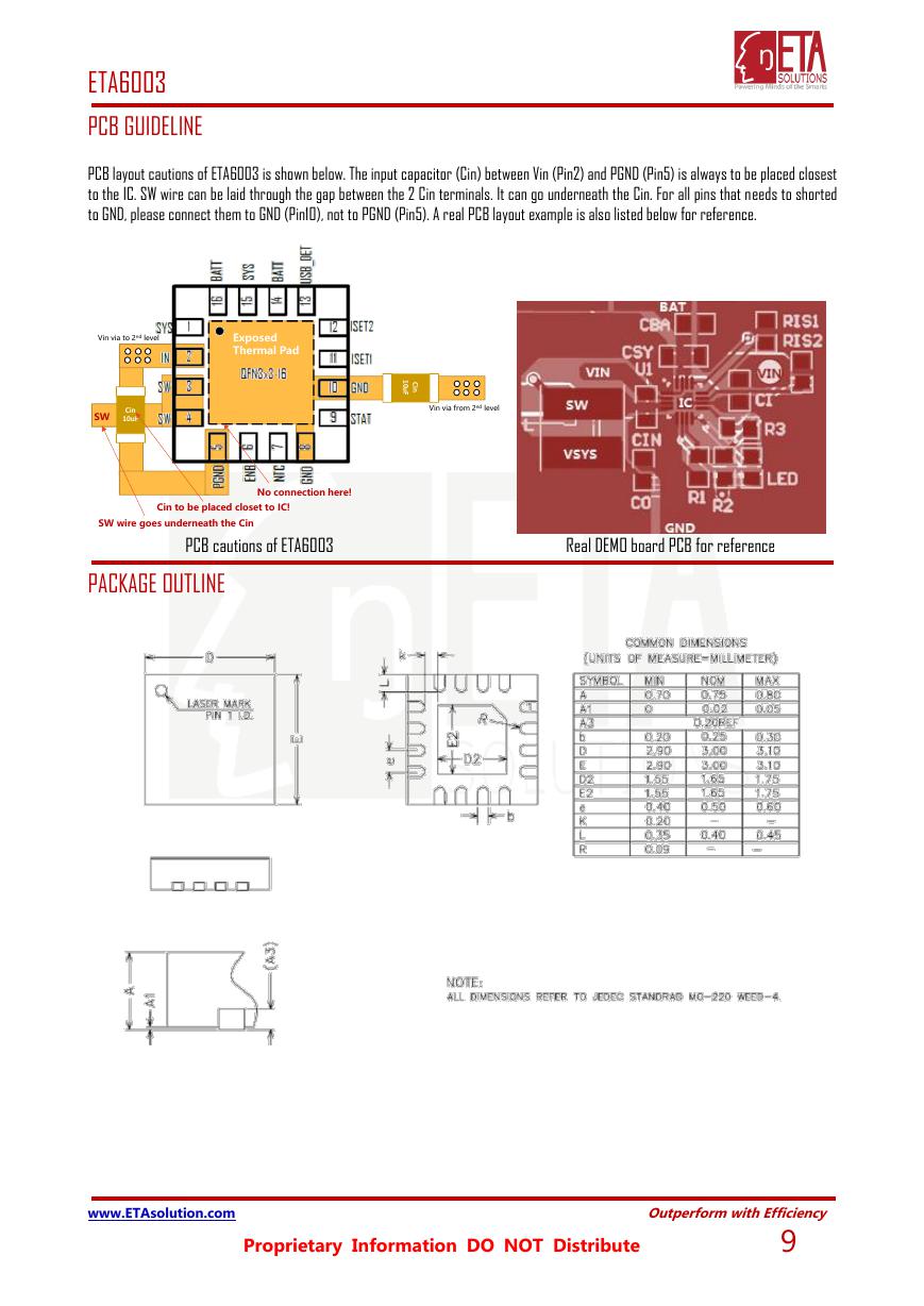
PCB GUIDELINE
PCB layout cautions of ETA6003 is shown below. The input capacitor (Cin) between Vin (Pin2) and PGND (Pin5) is always to be placed closest
to the IC. SW wire can be laid through the gap between the 2 Cin terminals. It can go underneath the Cin. For all pins that needs to shorted
to GND, please connect them to GND (Pin10), not to PGND (Pin5). A real PCB layout example is also listed below for reference.
PCB cautions of ETA6003 Real DEMO board PCB for reference
PACKAGE OUTLINE
www.ETAsolution.com Outperform with Efficiency
Proprietary Information DO NOT Distribute 9
Cin10uFExposed Thermal PadVinvia from 2ndlevelCin10uFNo connection here!Vinvia to 2ndlevelCinto be placed closet to IC!SWSW wire goes underneath the Cin�


 V2版本原理图(Capacitive-Fingerprint-Reader-Schematic_V2).pdf
 摄像头工作原理.doc
 VL53L0X简要说明(En.FLVL53L00216).pdf
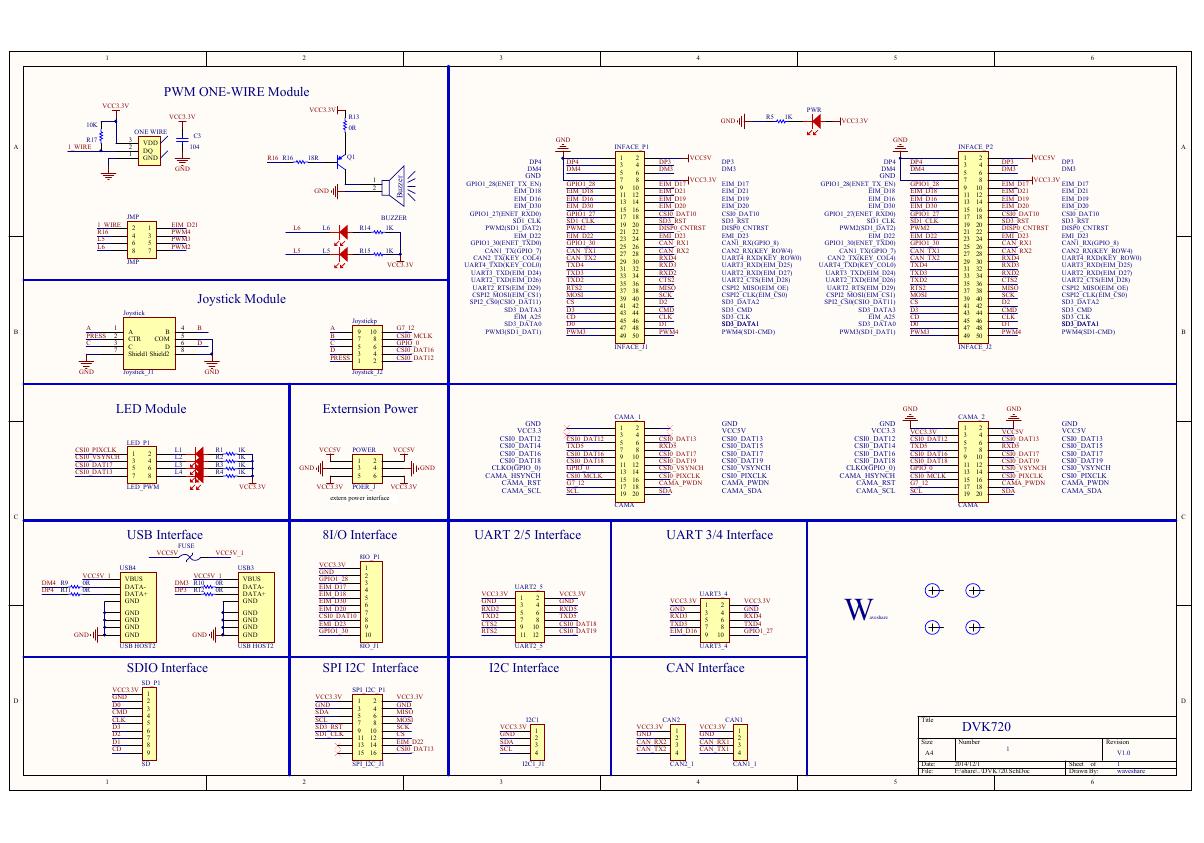 原理图(DVK720-Schematic).pdf
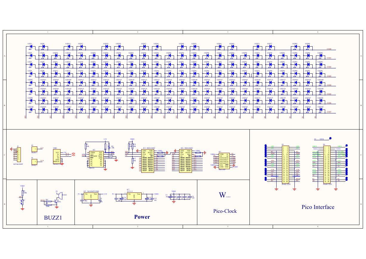 原理图(Pico-Clock-Green-Schdoc).pdf
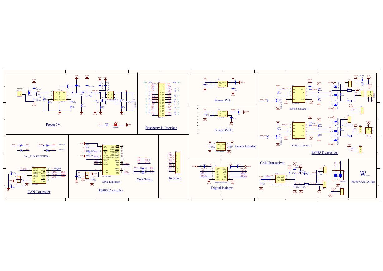 原理图(RS485-CAN-HAT-B-schematic).pdf
 File:SIM7500_SIM7600_SIM7800 Series_SSL_Application Note_V2.00.pdf
 ADS1263(Ads1262).pdf
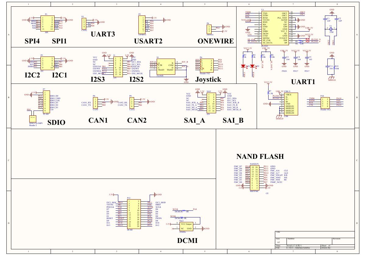 原理图(Open429Z-D-Schematic).pdf
 用户手册(Capacitive_Fingerprint_Reader_User_Manual_CN).pdf
 CY7C68013A(英文版)(CY7C68013A).pdf
 TechnicalReference_Dem.pdf