logo资料库

STM32F411数据手册.pdf

第1页 / 共146页
第2页 / 共146页
第3页 / 共146页
第4页 / 共146页
第5页 / 共146页
第6页 / 共146页
第7页 / 共146页
第8页 / 共146页
资料共146页,剩余部分请下载后查看
Table 1. Device summary
1 Introduction
2 Description
Table 2. STM32F411xC/xE features and peripheral counts
2.1 Compatibility with STM32F4 series
3 Functional overview
3.1 ARM® Cortex®-M4 with FPU core with embedded Flash and SRAM
3.2 Adaptive real-time memory accelerator (ART Accelerator™)
3.3 Batch Acquisition mode (BAM)
3.4 Memory protection unit
3.5 Embedded Flash memory
3.6 CRC (cyclic redundancy check) calculation unit
3.7 Embedded SRAM
3.8 Multi-AHB bus matrix
3.9 DMA controller (DMA)
3.10 Nested vectored interrupt controller (NVIC)
3.11 External interrupt/event controller (EXTI)
3.12 Clocks and startup
3.13 Boot modes
3.14 Power supply schemes
3.15 Power supply supervisor
3.15.1 Internal reset ON
3.15.2 Internal reset OFF
3.16 Voltage regulator
3.16.1 Regulator ON
3.16.2 Regulator OFF
3.16.3 Regulator ON/OFF and internal power supply supervisor availability
Table 3. Regulator ON/OFF and internal power supply supervisor availability
3.17 Real-time clock (RTC) and backup registers
3.18 Low-power modes
3.19 VBAT operation
3.20 Timers and watchdogs
Table 4. Timer feature comparison
3.20.1 Advanced-control timers (TIM1)
3.20.2 General-purpose timers (TIMx)
3.20.3 Independent watchdog
3.20.4 Window watchdog
3.20.5 SysTick timer
3.21 Inter-integrated circuit interface (I2C)
Table 5. Comparison of I2C analog and digital filters
3.22 Universal synchronous/asynchronous receiver transmitters (USART)
Table 6. USART feature comparison
3.23 Serial peripheral interface (SPI)
3.24 Inter-integrated sound (I2S)
3.25 Audio PLL (PLLI2S)
3.26 Secure digital input/output interface (SDIO)
3.27 Universal serial bus on-the-go full-speed (OTG_FS)
3.28 General-purpose input/outputs (GPIOs)
3.29 Analog-to-digital converter (ADC)
3.30 Temperature sensor
3.31 Serial wire JTAG debug port (SWJ-DP)
3.32 Embedded Trace Macrocell™
4 Pinouts and pin description
Table 7. Legend/abbreviations used in the pinout table
Table 8. STM32F411xC/xE pin definitions (continued)
Table 9. Alternate function mapping
5 Memory mapping
Table 10. STM32F411xC/xE register boundary addresses
6 Electrical characteristics
6.1 Parameter conditions
6.1.1 Minimum and maximum values
6.1.2 Typical values
6.1.3 Typical curves
6.1.4 Loading capacitor
6.1.5 Pin input voltage
6.1.6 Power supply scheme
6.1.7 Current consumption measurement
6.2 Absolute maximum ratings
Table 11. Voltage characteristics
Table 12. Current characteristics
Table 13. Thermal characteristics
6.3 Operating conditions
6.3.1 General operating conditions
Table 14. General operating conditions
Table 15. Features depending on the operating power supply range
6.3.2 VCAP1/VCAP2 external capacitors
Table 16. VCAP1/VCAP2 operating conditions
6.3.3 Operating conditions at power-up/power-down (regulator ON)
Table 17. Operating conditions at power-up / power-down (regulator ON)
6.3.4 Operating conditions at power-up / power-down (regulator OFF)
Table 18. Operating conditions at power-up / power-down (regulator OFF)
6.3.5 Embedded reset and power control block characteristics
Table 19. Embedded reset and power control block characteristics
6.3.6 Supply current characteristics
Typical and maximum current consumption
Table 20. Typical and maximum current consumption, code with data processing (ART accelerator disabled) running from SRAM - VDD = 1.7 V
Table 21. Typical and maximum current consumption, code with data processing (ART accelerator disabled) running from SRAM - VDD = 3.6 V
Table 22. Typical and maximum current consumption in run mode, code with data processing (ART accelerator enabled except prefetch) running from Flash memory- VDD = 1.7 V
Table 23. Typical and maximum current consumption in run mode, code with data processing (ART accelerator enabled except prefetch) running from Flash memory - VDD = 3.6 V
Table 24. Typical and maximum current consumption in run mode, code with data processing (ART accelerator disabled) running from Flash memory - VDD = 3.6 V
Table 25. Typical and maximum current consumption in run mode, code with data processing (ART accelerator enabled with prefetch) running from Flash memory - VDD = 3.6 V
Table 26. Typical and maximum current consumption in Sleep mode - VDD = 3.6 V
Table 27. Typical and maximum current consumptions in Stop mode - VDD = 1.7 V
Table 28. Typical and maximum current consumption in Stop mode - VDD=3.6 V
Table 29. Typical and maximum current consumption in Standby mode - VDD= 1.7 V
Table 30. Typical and maximum current consumption in Standby mode - VDD= 3.6 V
Table 31. Typical and maximum current consumptions in VBAT mode
I/O system current consumption
The current consumption of the I/O system has two components: static and dynamic.
Table 32. Switching output I/O current consumption
On-chip peripheral current consumption
Table 33. Peripheral current consumption
6.3.7 Wakeup time from low-power modes
Table 34. Low-power mode wakeup timings(1)
6.3.8 External clock source characteristics
High-speed external user clock generated from an external source
Table 35. High-speed external user clock characteristics
Low-speed external user clock generated from an external source
Table 36. Low-speed external user clock characteristics
High-speed external clock generated from a crystal/ceramic resonator
Table 37. HSE 4-26 MHz oscillator characteristics
Low-speed external clock generated from a crystal/ceramic resonator
Table 38. LSE oscillator characteristics (fLSE = 32.768 kHz)
6.3.9 Internal clock source characteristics
High-speed internal (HSI) RC oscillator
Table 39. HSI oscillator characteristics
Low-speed internal (LSI) RC oscillator
Table 40. LSI oscillator characteristics
6.3.10 PLL characteristics
Table 41. Main PLL characteristics
Table 42. PLLI2S (audio PLL) characteristics
6.3.11 PLL spread spectrum clock generation (SSCG) characteristics
Table 43. SSCG parameter constraints
6.3.12 Memory characteristics
Flash memory
Table 44. Flash memory characteristics
Table 45. Flash memory programming
Table 46. Flash memory programming with VPP voltage
Table 47. Flash memory endurance and data retention
6.3.13 EMC characteristics
Functional EMS (electromagnetic susceptibility)
Table 48. EMS characteristics for LQFP100 package
Designing hardened software to avoid noise problems
Electromagnetic Interference (EMI)
Table 49. EMI characteristics for LQFP100
6.3.14 Absolute maximum ratings (electrical sensitivity)
Electrostatic discharge (ESD)
Table 50. ESD absolute maximum ratings
Static latchup
Table 51. Electrical sensitivities
6.3.15 I/O current injection characteristics
Functional susceptibility to I/O current injection
Table 52. I/O current injection susceptibility
6.3.16 I/O port characteristics
General input/output characteristics
Table 53. I/O static characteristics
Output driving current
Output voltage levels
Table 54. Output voltage characteristics
Input/output AC characteristics
Table 55. I/O AC characteristics
6.3.17 NRST pin characteristics
Table 56. NRST pin characteristics
6.3.18 TIM timer characteristics
Table 57. TIMx characteristics
6.3.19 Communications interfaces
I2C interface characteristics
Table 58. I2C characteristics
Table 59. SCL frequency (fPCLK1= 50 MHz, VDD = VDD_I2C = 3.3 V)
SPI interface characteristics
Table 60. SPI dynamic characteristics
I2S interface characteristics
Table 61. I2S dynamic characteristics
USB OTG full speed (FS) characteristics
Table 62. USB OTG FS startup time
Table 63. USB OTG FS DC electrical characteristics
Table 64. USB OTG FS electrical characteristics
6.3.20 12-bit ADC characteristics
Table 65. ADC characteristics
Table 66. ADC accuracy at fADC = 18 MHz
Table 67. ADC accuracy at fADC = 30 MHz
Table 68. ADC accuracy at fADC = 36 MHz
Table 69. ADC dynamic accuracy at fADC = 18 MHz - limited test conditions
Table 70. ADC dynamic accuracy at fADC = 36 MHz - limited test conditions
General PCB design guidelines
6.3.21 Temperature sensor characteristics
Table 71. Temperature sensor characteristics
Table 72. Temperature sensor calibration values
6.3.22 VBAT monitoring characteristics
Table 73. VBAT monitoring characteristics
6.3.23 Embedded reference voltage
Table 74. Embedded internal reference voltage
Table 75. Internal reference voltage calibration values
6.3.24 SD/SDIO MMC/eMMC card host interface (SDIO) characteristics
Table 76. Dynamic characteristics: SD / MMC characteristics
Table 77. Dynamic characteristics: eMMC characteristics VDD = 1.7 V to 1.9 V
6.3.25 RTC characteristics
Table 78. RTC characteristics
7 Package characteristics
7.1 Package mechanical data
7.1.1 WLCSP49, 3.034 x 3.22 mm, 0.4 mm pitch wafer level chip scale package
Table 79. STM32F411xC/xE WLCSP49 wafer level chip scale package mechanical data
Table 80. WLCSP49 recommended PCB design rules (0.4 mm pitch)
Device marking
7.1.2 UFQFPN48, 7 x 7 mm, 0.5 mm pitch package
Table 81. UFQFPN48, 7 x 7 mm, 0.5 mm pitch, package mechanical data
Device marking
7.1.3 LQFP64, 10 x 10 mm, 64-pin low-profile quad flat package
Table 82. LQFP64, 10 x 10 mm, 64-pin low-profile quad flat package mechanical data
Device marking
7.1.4 LQFP100, 14 x 14 mm, 100-pin low-profile quad flat package
Table 83. LQPF100, 14 x 14 mm, 100-pin low-profile quad flat package mechanical data
Device marking
7.1.5 UFBGA100, 7 x 7 mm, 0.5 mm pitch package
Table 84. UFBGA100, 7 x 7 mm, 0.50 mm pitch, ultra fine pitch ball grid array package mechanical data
Device marking
7.2 Thermal characteristics
7.2.1 Reference document
8 Part numbering
Table 85. Ordering information scheme
Table 86. Device order codes
Appendix A Recommendations when using the internal reset OFF
A.1 Operating conditions
Table 87. Limitations depending on the operating power supply range
Appendix B Application block diagrams
B.1 USB OTG Full Speed (FS) interface solutions
B.2 Sensor Hub application example
B.3 Batch Acquisition Mode (BAM) example
9 Revision history
Table 88. Document revision history
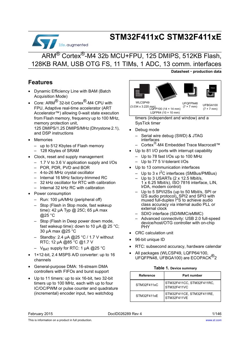
STM32F411xC STM32F411xE ARM® Cortex®-M4 32b MCU+FPU, 125 DMIPS, 512KB Flash, 128KB RAM, USB OTG FS, 11 TIMs, 1 ADC, 13 comm. interfaces Datasheet - production data Acquisition Mode) Features • Dynamic Efficiency Line with BAM (Batch • Core: ARM® 32-bit Cortex®-M4 CPU with FPU, Adaptive real-time accelerator (ART Accelerator™) allowing 0-wait state execution from Flash memory, frequency up to 100 MHz, memory protection unit, 125 DMIPS/1.25 DMIPS/MHz (Dhrystone 2.1), and DSP instructions • Memories – up to 512 Kbytes of Flash memory – 128 Kbytes of SRAM • Clock, reset and supply management – 1.7 V to 3.6 V application supply and I/Os – POR, PDR, PVD and BOR – 4-to-26 MHz crystal oscillator – Internal 16 MHz factory-trimmed RC – 32 kHz oscillator for RTC with calibration – Internal 32 kHz RC with calibration • Power consumption – Run: 100 µA/MHz (peripheral off) – Stop (Flash in Stop mode, fast wakeup time): 42 µA Typ @ 25C; 65 µA max @25 °C – Stop (Flash in Deep power down mode, fast wakeup time): down to 10 µA @ 25 °C; 30 µA max @25 °C – Standby: 2.4 µA @25 °C / 1.7 V without RTC; 12 µA @85 °C @1.7 V – VBAT supply for RTC: 1 µA @25 °C • 1×12-bit, 2.4 MSPS A/D converter: up to 16 channels WLCSP49 WLCSP49 (3.034 x 3.220 mm) LQFP100 (14 × 14 mm) LQFP64 (10 × 10 mm) UFQFPN48 (7 × 7 mm) UFBGA100 (7 × 7 mm) timers (independent and window) and a SysTick timer • Debug mode – Serial wire debug (SWD) & JTAG – Cortex®-M4 Embedded Trace Macrocell™ interfaces • Up to 81 I/O ports with interrupt capability – Up to 78 fast I/Os up to 100 MHz – Up to 77 5 V-tolerant I/Os • Up to 13 communication interfaces – Up to 3 x I2C interfaces (SMBus/PMBus) – Up to 3 USARTs (2 x 12.5 Mbit/s, 1 x 6.25 Mbit/s), ISO 7816 interface, LIN, IrDA, modem control) – Up to 5 SPI/I2Ss (up to 50 Mbit/s, SPI or I2S audio protocol), SPI2 and SPI3 with muxed full-duplex I2S to achieve audio class accuracy via internal audio PLL or external clock – SDIO interface (SD/MMC/eMMC) – Advanced connectivity: USB 2.0 full-speed device/host/OTG controller with on-chip PHY • CRC calculation unit • 96-bit unique ID • RTC: subsecond accuracy, hardware calendar • All packages (WLCSP49, LQFP64/100, UFQFPN48, UFBGA100) are ECOPACK®2 • General-purpose DMA: 16-stream DMA controllers with FIFOs and burst support • Up to 11 timers: up to six 16-bit, two 32-bit timers up to 100 MHz, each with up to four IC/OC/PWM or pulse counter and quadrature (incremental) encoder input, two watchdog Table 1. Device summary Reference Part number STM32F411xC STM32F411xE STM32F411CC, STM32F411RC, STM32F411VC STM32F411CE, STM32F411RE, STM32F411VE February 2015 This is information on a product in full production. DocID026289 Rev 4 1/146 www.st.com
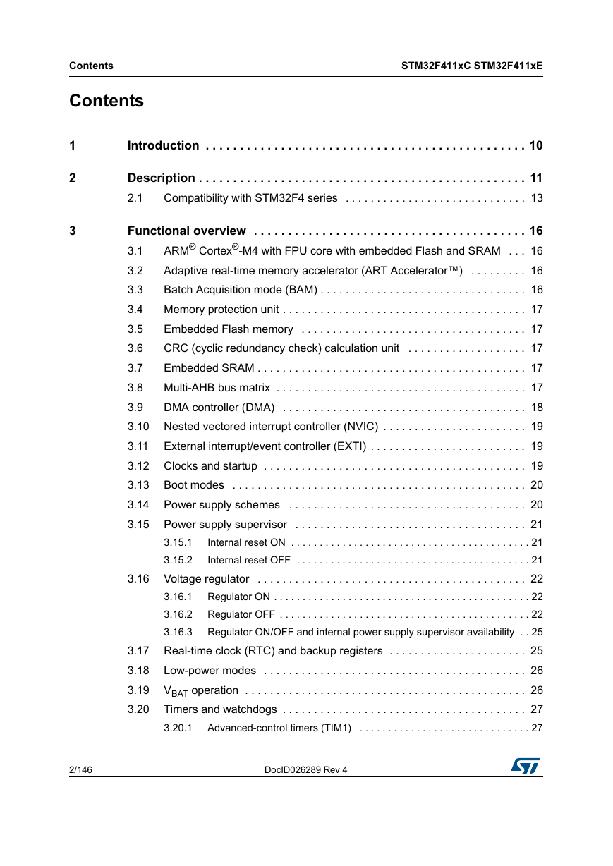
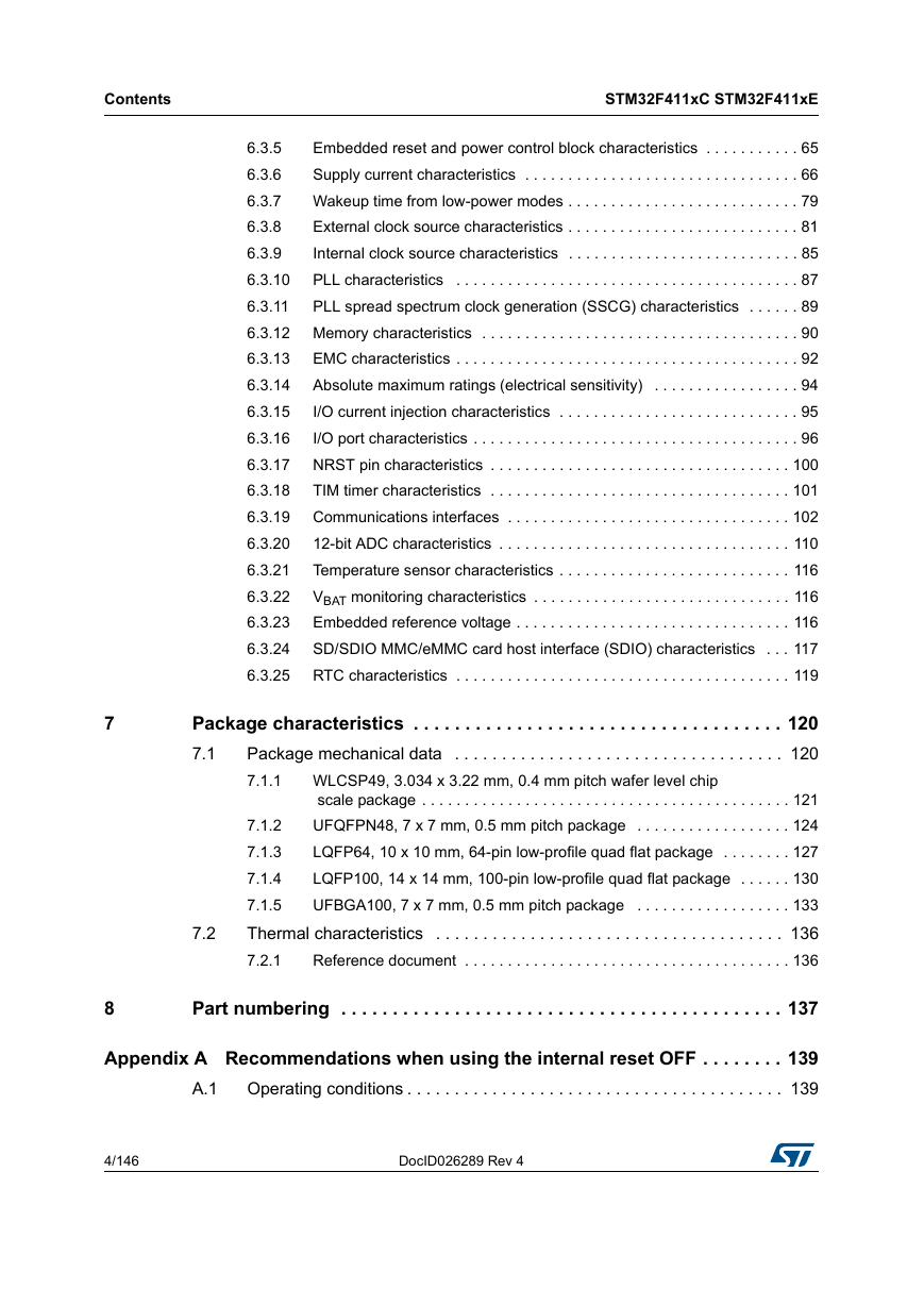
Contents Contents STM32F411xC STM32F411xE 1 2 3 Introduction . . . . . . . . . . . . . . . . . . . . . . . . . . . . . . . . . . . . . . . . . . . . . . . 10 Description . . . . . . . . . . . . . . . . . . . . . . . . . . . . . . . . . . . . . . . . . . . . . . . . 11 Compatibility with STM32F4 series . . . . . . . . . . . . . . . . . . . . . . . . . . . . . 13 2.1 Functional overview . . . . . . . . . . . . . . . . . . . . . . . . . . . . . . . . . . . . . . . . 16 ARM® Cortex®-M4 with FPU core with embedded Flash and SRAM . . . 16 3.1 Adaptive real-time memory accelerator (ART Accelerator™) . . . . . . . . . 16 3.2 3.3 Batch Acquisition mode (BAM) . . . . . . . . . . . . . . . . . . . . . . . . . . . . . . . . . 16 Memory protection unit . . . . . . . . . . . . . . . . . . . . . . . . . . . . . . . . . . . . . . . 17 3.4 3.5 Embedded Flash memory . . . . . . . . . . . . . . . . . . . . . . . . . . . . . . . . . . . . 17 CRC (cyclic redundancy check) calculation unit . . . . . . . . . . . . . . . . . . . 17 3.6 Embedded SRAM . . . . . . . . . . . . . . . . . . . . . . . . . . . . . . . . . . . . . . . . . . . 17 3.7 3.8 Multi-AHB bus matrix . . . . . . . . . . . . . . . . . . . . . . . . . . . . . . . . . . . . . . . . 17 3.9 DMA controller (DMA) . . . . . . . . . . . . . . . . . . . . . . . . . . . . . . . . . . . . . . . 18 3.10 Nested vectored interrupt controller (NVIC) . . . . . . . . . . . . . . . . . . . . . . . 19 3.11 External interrupt/event controller (EXTI) . . . . . . . . . . . . . . . . . . . . . . . . . 19 3.12 Clocks and startup . . . . . . . . . . . . . . . . . . . . . . . . . . . . . . . . . . . . . . . . . . 19 3.13 Boot modes . . . . . . . . . . . . . . . . . . . . . . . . . . . . . . . . . . . . . . . . . . . . . . . 20 3.14 Power supply schemes . . . . . . . . . . . . . . . . . . . . . . . . . . . . . . . . . . . . . . 20 3.15 Power supply supervisor . . . . . . . . . . . . . . . . . . . . . . . . . . . . . . . . . . . . . 21 Internal reset ON . . . . . . . . . . . . . . . . . . . . . . . . . . . . . . . . . . . . . . . . . . 21 Internal reset OFF . . . . . . . . . . . . . . . . . . . . . . . . . . . . . . . . . . . . . . . . . 21 3.16 Voltage regulator . . . . . . . . . . . . . . . . . . . . . . . . . . . . . . . . . . . . . . . . . . . 22 Regulator ON . . . . . . . . . . . . . . . . . . . . . . . . . . . . . . . . . . . . . . . . . . . . . 22 Regulator OFF . . . . . . . . . . . . . . . . . . . . . . . . . . . . . . . . . . . . . . . . . . . . 22 Regulator ON/OFF and internal power supply supervisor availability . . 25 3.17 Real-time clock (RTC) and backup registers . . . . . . . . . . . . . . . . . . . . . . 25 3.18 Low-power modes . . . . . . . . . . . . . . . . . . . . . . . . . . . . . . . . . . . . . . . . . . 26 3.19 VBAT operation . . . . . . . . . . . . . . . . . . . . . . . . . . . . . . . . . . . . . . . . . . . . . 26 Timers and watchdogs . . . . . . . . . . . . . . . . . . . . . . . . . . . . . . . . . . . . . . . 27 3.20 3.20.1 Advanced-control timers (TIM1) . . . . . . . . . . . . . . . . . . . . . . . . . . . . . . 27 3.16.1 3.16.2 3.16.3 3.15.1 3.15.2 2/146 DocID026289 Rev 4
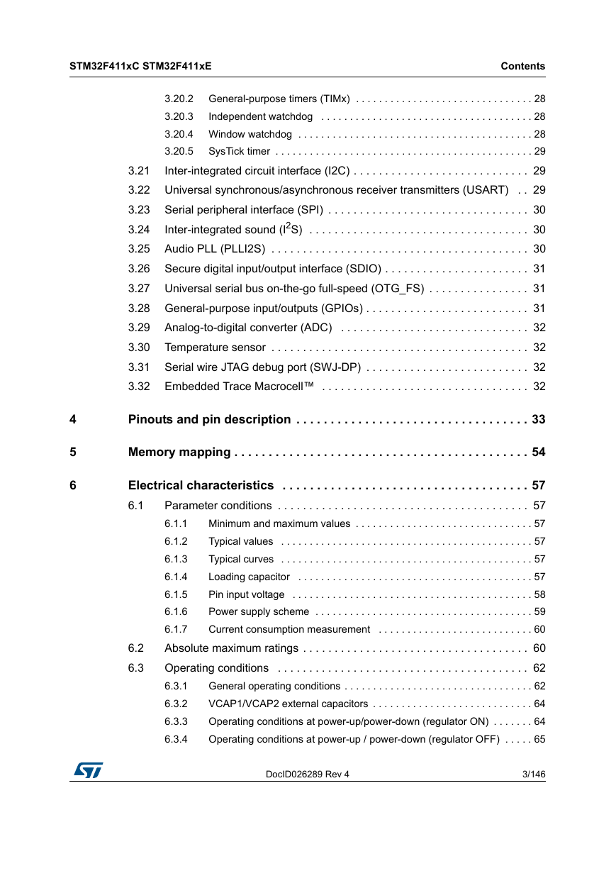
STM32F411xC STM32F411xE Contents 4 5 6 3.20.2 General-purpose timers (TIMx) . . . . . . . . . . . . . . . . . . . . . . . . . . . . . . . 28 3.20.3 Independent watchdog . . . . . . . . . . . . . . . . . . . . . . . . . . . . . . . . . . . . . 28 3.20.4 Window watchdog . . . . . . . . . . . . . . . . . . . . . . . . . . . . . . . . . . . . . . . . . 28 3.20.5 SysTick timer . . . . . . . . . . . . . . . . . . . . . . . . . . . . . . . . . . . . . . . . . . . . . 29 3.21 Inter-integrated circuit interface (I2C) . . . . . . . . . . . . . . . . . . . . . . . . . . . . 29 3.22 Universal synchronous/asynchronous receiver transmitters (USART) . . 29 3.23 Serial peripheral interface (SPI) . . . . . . . . . . . . . . . . . . . . . . . . . . . . . . . . 30 Inter-integrated sound (I2S) . . . . . . . . . . . . . . . . . . . . . . . . . . . . . . . . . . . 30 3.24 3.25 Audio PLL (PLLI2S) . . . . . . . . . . . . . . . . . . . . . . . . . . . . . . . . . . . . . . . . . 30 3.26 Secure digital input/output interface (SDIO) . . . . . . . . . . . . . . . . . . . . . . . 31 3.27 Universal serial bus on-the-go full-speed (OTG_FS) . . . . . . . . . . . . . . . . 31 3.28 General-purpose input/outputs (GPIOs) . . . . . . . . . . . . . . . . . . . . . . . . . . 31 3.29 Analog-to-digital converter (ADC) . . . . . . . . . . . . . . . . . . . . . . . . . . . . . . 32 3.30 Temperature sensor . . . . . . . . . . . . . . . . . . . . . . . . . . . . . . . . . . . . . . . . . 32 3.31 Serial wire JTAG debug port (SWJ-DP) . . . . . . . . . . . . . . . . . . . . . . . . . . 32 3.32 Embedded Trace Macrocell™ . . . . . . . . . . . . . . . . . . . . . . . . . . . . . . . . . 32 Pinouts and pin description . . . . . . . . . . . . . . . . . . . . . . . . . . . . . . . . . . 33 Memory mapping . . . . . . . . . . . . . . . . . . . . . . . . . . . . . . . . . . . . . . . . . . . 54 Electrical characteristics . . . . . . . . . . . . . . . . . . . . . . . . . . . . . . . . . . . . 57 Parameter conditions . . . . . . . . . . . . . . . . . . . . . . . . . . . . . . . . . . . . . . . . 57 6.1 Minimum and maximum values . . . . . . . . . . . . . . . . . . . . . . . . . . . . . . . 57 6.1.1 6.1.2 Typical values . . . . . . . . . . . . . . . . . . . . . . . . . . . . . . . . . . . . . . . . . . . . 57 Typical curves . . . . . . . . . . . . . . . . . . . . . . . . . . . . . . . . . . . . . . . . . . . . 57 6.1.3 Loading capacitor . . . . . . . . . . . . . . . . . . . . . . . . . . . . . . . . . . . . . . . . . 57 6.1.4 6.1.5 Pin input voltage . . . . . . . . . . . . . . . . . . . . . . . . . . . . . . . . . . . . . . . . . . 58 Power supply scheme . . . . . . . . . . . . . . . . . . . . . . . . . . . . . . . . . . . . . . 59 6.1.6 6.1.7 Current consumption measurement . . . . . . . . . . . . . . . . . . . . . . . . . . . 60 Absolute maximum ratings . . . . . . . . . . . . . . . . . . . . . . . . . . . . . . . . . . . . 60 Operating conditions . . . . . . . . . . . . . . . . . . . . . . . . . . . . . . . . . . . . . . . . 62 General operating conditions . . . . . . . . . . . . . . . . . . . . . . . . . . . . . . . . . 62 6.3.1 6.3.2 VCAP1/VCAP2 external capacitors . . . . . . . . . . . . . . . . . . . . . . . . . . . . 64 Operating conditions at power-up/power-down (regulator ON) . . . . . . . 64 6.3.3 6.3.4 Operating conditions at power-up / power-down (regulator OFF) . . . . . 65 6.2 6.3 DocID026289 Rev 4 3/146 5
Contents STM32F411xC STM32F411xE Embedded reset and power control block characteristics . . . . . . . . . . . 65 6.3.5 Supply current characteristics . . . . . . . . . . . . . . . . . . . . . . . . . . . . . . . . 66 6.3.6 Wakeup time from low-power modes . . . . . . . . . . . . . . . . . . . . . . . . . . . 79 6.3.7 External clock source characteristics . . . . . . . . . . . . . . . . . . . . . . . . . . . 81 6.3.8 Internal clock source characteristics . . . . . . . . . . . . . . . . . . . . . . . . . . . 85 6.3.9 PLL characteristics . . . . . . . . . . . . . . . . . . . . . . . . . . . . . . . . . . . . . . . . 87 6.3.10 6.3.11 PLL spread spectrum clock generation (SSCG) characteristics . . . . . . 89 6.3.12 Memory characteristics . . . . . . . . . . . . . . . . . . . . . . . . . . . . . . . . . . . . . 90 6.3.13 EMC characteristics . . . . . . . . . . . . . . . . . . . . . . . . . . . . . . . . . . . . . . . . 92 Absolute maximum ratings (electrical sensitivity) . . . . . . . . . . . . . . . . . 94 6.3.14 I/O current injection characteristics . . . . . . . . . . . . . . . . . . . . . . . . . . . . 95 6.3.15 6.3.16 I/O port characteristics . . . . . . . . . . . . . . . . . . . . . . . . . . . . . . . . . . . . . . 96 NRST pin characteristics . . . . . . . . . . . . . . . . . . . . . . . . . . . . . . . . . . . 100 6.3.17 TIM timer characteristics . . . . . . . . . . . . . . . . . . . . . . . . . . . . . . . . . . . 101 6.3.18 6.3.19 Communications interfaces . . . . . . . . . . . . . . . . . . . . . . . . . . . . . . . . . 102 12-bit ADC characteristics . . . . . . . . . . . . . . . . . . . . . . . . . . . . . . . . . . 110 6.3.20 6.3.21 Temperature sensor characteristics . . . . . . . . . . . . . . . . . . . . . . . . . . . 116 VBAT monitoring characteristics . . . . . . . . . . . . . . . . . . . . . . . . . . . . . . 116 6.3.22 Embedded reference voltage . . . . . . . . . . . . . . . . . . . . . . . . . . . . . . . . 116 6.3.23 SD/SDIO MMC/eMMC card host interface (SDIO) characteristics . . . 117 6.3.24 6.3.25 RTC characteristics . . . . . . . . . . . . . . . . . . . . . . . . . . . . . . . . . . . . . . . 119 7 Package characteristics . . . . . . . . . . . . . . . . . . . . . . . . . . . . . . . . . . . . 120 Package mechanical data . . . . . . . . . . . . . . . . . . . . . . . . . . . . . . . . . . . 120 7.1 7.1.1 WLCSP49, 3.034 x 3.22 mm, 0.4 mm pitch wafer level chip scale package . . . . . . . . . . . . . . . . . . . . . . . . . . . . . . . . . . . . . . . . . . . 121 7.1.2 UFQFPN48, 7 x 7 mm, 0.5 mm pitch package . . . . . . . . . . . . . . . . . . 124 7.1.3 LQFP64, 10 x 10 mm, 64-pin low-profile quad flat package . . . . . . . . 127 7.1.4 LQFP100, 14 x 14 mm, 100-pin low-profile quad flat package . . . . . . 130 7.1.5 UFBGA100, 7 x 7 mm, 0.5 mm pitch package . . . . . . . . . . . . . . . . . . 133 Thermal characteristics . . . . . . . . . . . . . . . . . . . . . . . . . . . . . . . . . . . . . 136 7.2.1 Reference document . . . . . . . . . . . . . . . . . . . . . . . . . . . . . . . . . . . . . . 136 7.2 8 Part numbering . . . . . . . . . . . . . . . . . . . . . . . . . . . . . . . . . . . . . . . . . . . 137 Appendix A Recommendations when using the internal reset OFF . . . . . . . . 139 Operating conditions . . . . . . . . . . . . . . . . . . . . . . . . . . . . . . . . . . . . . . . . 139 A.1 4/146 DocID026289 Rev 4
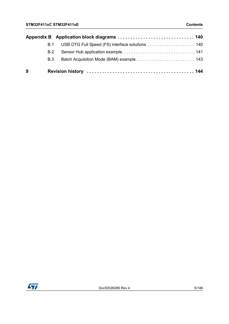
STM32F411xC STM32F411xE Contents Appendix B Application block diagrams . . . . . . . . . . . . . . . . . . . . . . . . . . . . . . 140 USB OTG Full Speed (FS) interface solutions . . . . . . . . . . . . . . . . . . . . 140 Sensor Hub application example. . . . . . . . . . . . . . . . . . . . . . . . . . . . . . . 141 Batch Acquisition Mode (BAM) example. . . . . . . . . . . . . . . . . . . . . . . . . 143 B.1 B.2 B.3 9 Revision history . . . . . . . . . . . . . . . . . . . . . . . . . . . . . . . . . . . . . . . . . . 144 DocID026289 Rev 4 5/146 5
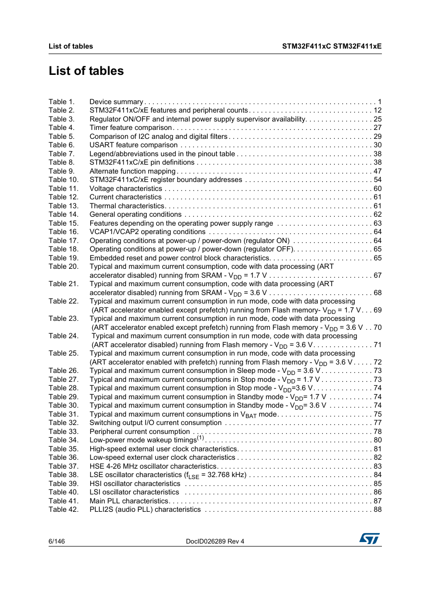
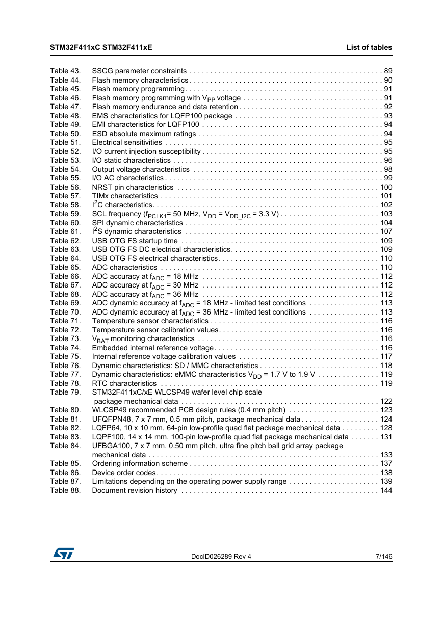
List of tables List of tables STM32F411xC STM32F411xE Table 21. Table 1. Device summary . . . . . . . . . . . . . . . . . . . . . . . . . . . . . . . . . . . . . . . . . . . . . . . . . . . . . . . . . . 1 Table 2. STM32F411xC/xE features and peripheral counts. . . . . . . . . . . . . . . . . . . . . . . . . . . . . . . 12 Table 3. Regulator ON/OFF and internal power supply supervisor availability. . . . . . . . . . . . . . . . . 25 Table 4. Timer feature comparison. . . . . . . . . . . . . . . . . . . . . . . . . . . . . . . . . . . . . . . . . . . . . . . . . . 27 Table 5. Comparison of I2C analog and digital filters . . . . . . . . . . . . . . . . . . . . . . . . . . . . . . . . . . . . 29 Table 6. USART feature comparison . . . . . . . . . . . . . . . . . . . . . . . . . . . . . . . . . . . . . . . . . . . . . . . . 30 Table 7. Legend/abbreviations used in the pinout table . . . . . . . . . . . . . . . . . . . . . . . . . . . . . . . . . . 38 Table 8. STM32F411xC/xE pin definitions . . . . . . . . . . . . . . . . . . . . . . . . . . . . . . . . . . . . . . . . . . . . 38 Table 9. Alternate function mapping . . . . . . . . . . . . . . . . . . . . . . . . . . . . . . . . . . . . . . . . . . . . . . . . . 47 Table 10. STM32F411xC/xE register boundary addresses . . . . . . . . . . . . . . . . . . . . . . . . . . . . . . . . 54 Table 11. Voltage characteristics . . . . . . . . . . . . . . . . . . . . . . . . . . . . . . . . . . . . . . . . . . . . . . . . . . . . 60 Table 12. Current characteristics . . . . . . . . . . . . . . . . . . . . . . . . . . . . . . . . . . . . . . . . . . . . . . . . . . . . 61 Table 13. Thermal characteristics. . . . . . . . . . . . . . . . . . . . . . . . . . . . . . . . . . . . . . . . . . . . . . . . . . . . 61 Table 14. General operating conditions . . . . . . . . . . . . . . . . . . . . . . . . . . . . . . . . . . . . . . . . . . . . . . . 62 Features depending on the operating power supply range . . . . . . . . . . . . . . . . . . . . . . . . 63 Table 15. Table 16. VCAP1/VCAP2 operating conditions . . . . . . . . . . . . . . . . . . . . . . . . . . . . . . . . . . . . . . . . . 64 Table 17. Operating conditions at power-up / power-down (regulator ON) . . . . . . . . . . . . . . . . . . . . 64 Table 18. Operating conditions at power-up / power-down (regulator OFF). . . . . . . . . . . . . . . . . . . . 65 Embedded reset and power control block characteristics. . . . . . . . . . . . . . . . . . . . . . . . . . 65 Table 19. Typical and maximum current consumption, code with data processing (ART Table 20. accelerator disabled) running from SRAM - VDD = 1.7 V . . . . . . . . . . . . . . . . . . . . . . . . . . 67 Typical and maximum current consumption, code with data processing (ART accelerator disabled) running from SRAM - VDD = 3.6 V . . . . . . . . . . . . . . . . . . . . . . . . . . 68 Typical and maximum current consumption in run mode, code with data processing (ART accelerator enabled except prefetch) running from Flash memory- VDD = 1.7 V. . . 69 Typical and maximum current consumption in run mode, code with data processing (ART accelerator enabled except prefetch) running from Flash memory - VDD = 3.6 V . . 70 Typical and maximum current consumption in run mode, code with data processing (ART accelerator disabled) running from Flash memory - VDD = 3.6 V. . . . . . . . . . . . . . . 71 Typical and maximum current consumption in run mode, code with data processing (ART accelerator enabled with prefetch) running from Flash memory - VDD = 3.6 V . . . . . 72 Table 26. Typical and maximum current consumption in Sleep mode - VDD = 3.6 V . . . . . . . . . . . . . 73 Table 27. Typical and maximum current consumptions in Stop mode - VDD = 1.7 V . . . . . . . . . . . . . 73 Table 28. Typical and maximum current consumption in Stop mode - VDD=3.6 V. . . . . . . . . . . . . . . 74 Table 29. Typical and maximum current consumption in Standby mode - VDD= 1.7 V . . . . . . . . . . . 74 Table 30. Typical and maximum current consumption in Standby mode - VDD= 3.6 V . . . . . . . . . . . 74 Table 31. Typical and maximum current consumptions in VBAT mode. . . . . . . . . . . . . . . . . . . . . . . . 75 Table 32. Switching output I/O current consumption . . . . . . . . . . . . . . . . . . . . . . . . . . . . . . . . . . . . . 77 Table 33. Peripheral current consumption . . . . . . . . . . . . . . . . . . . . . . . . . . . . . . . . . . . . . . . . . . . . . 78 Low-power mode wakeup timings(1) . . . . . . . . . . . . . . . . . . . . . . . . . . . . . . . . . . . . . . . . . . 80 Table 34. Table 35. High-speed external user clock characteristics. . . . . . . . . . . . . . . . . . . . . . . . . . . . . . . . . . 81 Table 36. Low-speed external user clock characteristics . . . . . . . . . . . . . . . . . . . . . . . . . . . . . . . . . . 82 Table 37. HSE 4-26 MHz oscillator characteristics. . . . . . . . . . . . . . . . . . . . . . . . . . . . . . . . . . . . . . . 83 Table 38. LSE oscillator characteristics (fLSE = 32.768 kHz) . . . . . . . . . . . . . . . . . . . . . . . . . . . . . . . 84 Table 39. HSI oscillator characteristics . . . . . . . . . . . . . . . . . . . . . . . . . . . . . . . . . . . . . . . . . . . . . . . 85 Table 40. LSI oscillator characteristics . . . . . . . . . . . . . . . . . . . . . . . . . . . . . . . . . . . . . . . . . . . . . . . 86 Table 41. Main PLL characteristics. . . . . . . . . . . . . . . . . . . . . . . . . . . . . . . . . . . . . . . . . . . . . . . . . . . 87 Table 42. PLLI2S (audio PLL) characteristics . . . . . . . . . . . . . . . . . . . . . . . . . . . . . . . . . . . . . . . . . . 88 Table 24. Table 22. Table 23. Table 25. 6/146 DocID026289 Rev 4
STM32F411xC STM32F411xE List of tables SSCG parameter constraints . . . . . . . . . . . . . . . . . . . . . . . . . . . . . . . . . . . . . . . . . . . . . . . 89 Table 43. Flash memory characteristics . . . . . . . . . . . . . . . . . . . . . . . . . . . . . . . . . . . . . . . . . . . . . . . 90 Table 44. Flash memory programming. . . . . . . . . . . . . . . . . . . . . . . . . . . . . . . . . . . . . . . . . . . . . . . . 91 Table 45. Flash memory programming with VPP voltage . . . . . . . . . . . . . . . . . . . . . . . . . . . . . . . . . . 91 Table 46. Flash memory endurance and data retention . . . . . . . . . . . . . . . . . . . . . . . . . . . . . . . . . . . 92 Table 47. EMS characteristics for LQFP100 package . . . . . . . . . . . . . . . . . . . . . . . . . . . . . . . . . . . . 93 Table 48. EMI characteristics for LQFP100 . . . . . . . . . . . . . . . . . . . . . . . . . . . . . . . . . . . . . . . . . . . . 94 Table 49. ESD absolute maximum ratings . . . . . . . . . . . . . . . . . . . . . . . . . . . . . . . . . . . . . . . . . . . . . 94 Table 50. Electrical sensitivities . . . . . . . . . . . . . . . . . . . . . . . . . . . . . . . . . . . . . . . . . . . . . . . . . . . . . 95 Table 51. I/O current injection susceptibility . . . . . . . . . . . . . . . . . . . . . . . . . . . . . . . . . . . . . . . . . . . . 95 Table 52. Table 53. I/O static characteristics . . . . . . . . . . . . . . . . . . . . . . . . . . . . . . . . . . . . . . . . . . . . . . . . . . . 96 Table 54. Output voltage characteristics . . . . . . . . . . . . . . . . . . . . . . . . . . . . . . . . . . . . . . . . . . . . . . 98 I/O AC characteristics . . . . . . . . . . . . . . . . . . . . . . . . . . . . . . . . . . . . . . . . . . . . . . . . . . . . . 99 Table 55. NRST pin characteristics . . . . . . . . . . . . . . . . . . . . . . . . . . . . . . . . . . . . . . . . . . . . . . . . . 100 Table 56. TIMx characteristics . . . . . . . . . . . . . . . . . . . . . . . . . . . . . . . . . . . . . . . . . . . . . . . . . . . . . 101 Table 57. I2C characteristics. . . . . . . . . . . . . . . . . . . . . . . . . . . . . . . . . . . . . . . . . . . . . . . . . . . . . . . 102 Table 58. SCL frequency (fPCLK1= 50 MHz, VDD = VDD_I2C = 3.3 V) . . . . . . . . . . . . . . . . . . . . . . . . 103 Table 59. Table 60. SPI dynamic characteristics . . . . . . . . . . . . . . . . . . . . . . . . . . . . . . . . . . . . . . . . . . . . . . . 104 I2S dynamic characteristics . . . . . . . . . . . . . . . . . . . . . . . . . . . . . . . . . . . . . . . . . . . . . . . 107 Table 61. USB OTG FS startup time . . . . . . . . . . . . . . . . . . . . . . . . . . . . . . . . . . . . . . . . . . . . . . . . 109 Table 62. Table 63. USB OTG FS DC electrical characteristics. . . . . . . . . . . . . . . . . . . . . . . . . . . . . . . . . . . . 109 USB OTG FS electrical characteristics. . . . . . . . . . . . . . . . . . . . . . . . . . . . . . . . . . . . . . . 110 Table 64. ADC characteristics . . . . . . . . . . . . . . . . . . . . . . . . . . . . . . . . . . . . . . . . . . . . . . . . . . . . . 110 Table 65. ADC accuracy at fADC = 18 MHz . . . . . . . . . . . . . . . . . . . . . . . . . . . . . . . . . . . . . . . . . . . 112 Table 66. Table 67. ADC accuracy at fADC = 30 MHz . . . . . . . . . . . . . . . . . . . . . . . . . . . . . . . . . . . . . . . . . . . 112 ADC accuracy at fADC = 36 MHz . . . . . . . . . . . . . . . . . . . . . . . . . . . . . . . . . . . . . . . . . . . 112 Table 68. ADC dynamic accuracy at fADC = 18 MHz - limited test conditions . . . . . . . . . . . . . . . . . 113 Table 69. ADC dynamic accuracy at fADC = 36 MHz - limited test conditions . . . . . . . . . . . . . . . . . 113 Table 70. Table 71. Temperature sensor characteristics . . . . . . . . . . . . . . . . . . . . . . . . . . . . . . . . . . . . . . . . . 116 Temperature sensor calibration values. . . . . . . . . . . . . . . . . . . . . . . . . . . . . . . . . . . . . . . 116 Table 72. VBAT monitoring characteristics . . . . . . . . . . . . . . . . . . . . . . . . . . . . . . . . . . . . . . . . . . . . 116 Table 73. Embedded internal reference voltage. . . . . . . . . . . . . . . . . . . . . . . . . . . . . . . . . . . . . . . . 116 Table 74. Table 75. Internal reference voltage calibration values . . . . . . . . . . . . . . . . . . . . . . . . . . . . . . . . . . 117 Dynamic characteristics: SD / MMC characteristics . . . . . . . . . . . . . . . . . . . . . . . . . . . . . 118 Table 76. Dynamic characteristics: eMMC characteristics VDD = 1.7 V to 1.9 V . . . . . . . . . . . . . . . 119 Table 77. Table 78. RTC characteristics . . . . . . . . . . . . . . . . . . . . . . . . . . . . . . . . . . . . . . . . . . . . . . . . . . . . . 119 STM32F411xC/xE WLCSP49 wafer level chip scale Table 79. package mechanical data . . . . . . . . . . . . . . . . . . . . . . . . . . . . . . . . . . . . . . . . . . . . . . . . 122 Table 80. WLCSP49 recommended PCB design rules (0.4 mm pitch) . . . . . . . . . . . . . . . . . . . . . . 123 UFQFPN48, 7 x 7 mm, 0.5 mm pitch, package mechanical data. . . . . . . . . . . . . . . . . . . 124 Table 81. Table 82. LQFP64, 10 x 10 mm, 64-pin low-profile quad flat package mechanical data . . . . . . . . . 128 LQPF100, 14 x 14 mm, 100-pin low-profile quad flat package mechanical data . . . . . . . 131 Table 83. UFBGA100, 7 x 7 mm, 0.50 mm pitch, ultra fine pitch ball grid array package Table 84. mechanical data . . . . . . . . . . . . . . . . . . . . . . . . . . . . . . . . . . . . . . . . . . . . . . . . . . . . . . . . 133 Table 85. Ordering information scheme . . . . . . . . . . . . . . . . . . . . . . . . . . . . . . . . . . . . . . . . . . . . . . 137 Table 86. Device order codes. . . . . . . . . . . . . . . . . . . . . . . . . . . . . . . . . . . . . . . . . . . . . . . . . . . . . . 138 Limitations depending on the operating power supply range . . . . . . . . . . . . . . . . . . . . . . 139 Table 87. Table 88. Document revision history . . . . . . . . . . . . . . . . . . . . . . . . . . . . . . . . . . . . . . . . . . . . . . . . 144 DocID026289 Rev 4 7/146 7
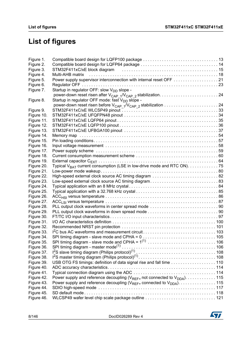
List of figures List of figures STM32F411xC STM32F411xE Figure 8. Figure 1. Figure 2. Figure 3. Figure 4. Figure 5. Figure 6. Figure 7. Compatible board design for LQFP100 package . . . . . . . . . . . . . . . . . . . . . . . . . . . . . . . . 13 Compatible board design for LQFP64 package . . . . . . . . . . . . . . . . . . . . . . . . . . . . . . . . . 14 STM32F411xC/xE block diagram . . . . . . . . . . . . . . . . . . . . . . . . . . . . . . . . . . . . . . . . . 15 Multi-AHB matrix . . . . . . . . . . . . . . . . . . . . . . . . . . . . . . . . . . . . . . . . . . . . . . . . . . . . . . . 18 Power supply supervisor interconnection with internal reset OFF . . . . . . . . . . . . . . . . . . . 21 Regulator OFF . . . . . . . . . . . . . . . . . . . . . . . . . . . . . . . . . . . . . . . . . . . . . . . . . . . . . . . . . . 23 Startup in regulator OFF: slow VDD slope - power-down reset risen after VCAP_1/VCAP_2 stabilization. . . . . . . . . . . . . . . . . . . . . . . . . 24 Startup in regulator OFF mode: fast VDD slope - power-down reset risen before VCAP_1/VCAP_2 stabilization . . . . . . . . . . . . . . . . . . . . . . . 24 Figure 9. STM32F411xC/xE WLCSP49 pinout . . . . . . . . . . . . . . . . . . . . . . . . . . . . . . . . . . . . . . . . . 33 Figure 10. STM32F411xC/xE UFQFPN48 pinout . . . . . . . . . . . . . . . . . . . . . . . . . . . . . . . . . . . . . . . . 34 Figure 11. STM32F411xC/xE LQFP64 pinout . . . . . . . . . . . . . . . . . . . . . . . . . . . . . . . . . . . . . . . . . . . 35 Figure 12. STM32F411xC/xE LQFP100 pinout . . . . . . . . . . . . . . . . . . . . . . . . . . . . . . . . . . . . . . . . . . 36 Figure 13. STM32F411xC/xE UFBGA100 pinout . . . . . . . . . . . . . . . . . . . . . . . . . . . . . . . . . . . . . . . . 37 Figure 14. Memory map . . . . . . . . . . . . . . . . . . . . . . . . . . . . . . . . . . . . . . . . . . . . . . . . . . . . . . . . . . . 54 Figure 15. Pin loading conditions. . . . . . . . . . . . . . . . . . . . . . . . . . . . . . . . . . . . . . . . . . . . . . . . . . . . . 57 Figure 16. Input voltage measurement . . . . . . . . . . . . . . . . . . . . . . . . . . . . . . . . . . . . . . . . . . . . . . . . 58 Figure 17. Power supply scheme . . . . . . . . . . . . . . . . . . . . . . . . . . . . . . . . . . . . . . . . . . . . . . . . . . . . 59 Figure 18. Current consumption measurement scheme . . . . . . . . . . . . . . . . . . . . . . . . . . . . . . . . . . . 60 Figure 19. External capacitor CEXT . . . . . . . . . . . . . . . . . . . . . . . . . . . . . . . . . . . . . . . . . . . . . . . . . . . 64 Figure 20. Typical VBAT current consumption (LSE in low-drive mode and RTC ON). . . . . . . . . . . . . 75 Figure 21. Low-power mode wakeup. . . . . . . . . . . . . . . . . . . . . . . . . . . . . . . . . . . . . . . . . . . . . . . . . . 80 Figure 22. High-speed external clock source AC timing diagram . . . . . . . . . . . . . . . . . . . . . . . . . . . . 82 Figure 23. Low-speed external clock source AC timing diagram. . . . . . . . . . . . . . . . . . . . . . . . . . . . . 83 Figure 24. Typical application with an 8 MHz crystal . . . . . . . . . . . . . . . . . . . . . . . . . . . . . . . . . . . . . . 84 Figure 25. Typical application with a 32.768 kHz crystal . . . . . . . . . . . . . . . . . . . . . . . . . . . . . . . . . . . 85 Figure 26. ACCHSI versus temperature . . . . . . . . . . . . . . . . . . . . . . . . . . . . . . . . . . . . . . . . . . . . . . . . 86 Figure 27. ACCLSI versus temperature . . . . . . . . . . . . . . . . . . . . . . . . . . . . . . . . . . . . . . . . . . . . . . . . 87 Figure 28. PLL output clock waveforms in center spread mode . . . . . . . . . . . . . . . . . . . . . . . . . . . . . 90 Figure 29. PLL output clock waveforms in down spread mode . . . . . . . . . . . . . . . . . . . . . . . . . . . . . . 90 Figure 30. FT/TC I/O input characteristics . . . . . . . . . . . . . . . . . . . . . . . . . . . . . . . . . . . . . . . . . . . . . . 97 Figure 31. I/O AC characteristics definition . . . . . . . . . . . . . . . . . . . . . . . . . . . . . . . . . . . . . . . . . . . . 100 Figure 32. Recommended NRST pin protection . . . . . . . . . . . . . . . . . . . . . . . . . . . . . . . . . . . . . . . . 101 I2C bus AC waveforms and measurement circuit . . . . . . . . . . . . . . . . . . . . . . . . . . . . . . . 103 Figure 33. Figure 34. SPI timing diagram - slave mode and CPHA = 0 . . . . . . . . . . . . . . . . . . . . . . . . . . . . . . . 105 Figure 35. SPI timing diagram - slave mode and CPHA = 1(1) . . . . . . . . . . . . . . . . . . . . . . . . . . . . . 106 Figure 36. SPI timing diagram - master mode(1) . . . . . . . . . . . . . . . . . . . . . . . . . . . . . . . . . . . . . . . . 106 I2S slave timing diagram (Philips protocol)(1) . . . . . . . . . . . . . . . . . . . . . . . . . . . . . . . . . . 108 Figure 37. I2S master timing diagram (Philips protocol)(1) . . . . . . . . . . . . . . . . . . . . . . . . . . . . . . . . . 108 Figure 38. Figure 39. USB OTG FS timings: definition of data signal rise and fall time . . . . . . . . . . . . . . . . . . . 110 Figure 40. ADC accuracy characteristics. . . . . . . . . . . . . . . . . . . . . . . . . . . . . . . . . . . . . . . . . . . . . . 114 Figure 41. Typical connection diagram using the ADC . . . . . . . . . . . . . . . . . . . . . . . . . . . . . . . . . . . 114 Figure 42. Power supply and reference decoupling (VREF+ not connected to VDDA). . . . . . . . . . . . . 115 Figure 43. Power supply and reference decoupling (VREF+ connected to VDDA). . . . . . . . . . . . . . . . 115 Figure 44. SDIO high-speed mode . . . . . . . . . . . . . . . . . . . . . . . . . . . . . . . . . . . . . . . . . . . . . . . . . . 117 Figure 45. SD default mode . . . . . . . . . . . . . . . . . . . . . . . . . . . . . . . . . . . . . . . . . . . . . . . . . . . . . . . . 118 Figure 46. WLCSP49 wafer level chip scale package outline . . . . . . . . . . . . . . . . . . . . . . . . . . . . . . 121 8/146 DocID026289 Rev 4
分享到:
收藏