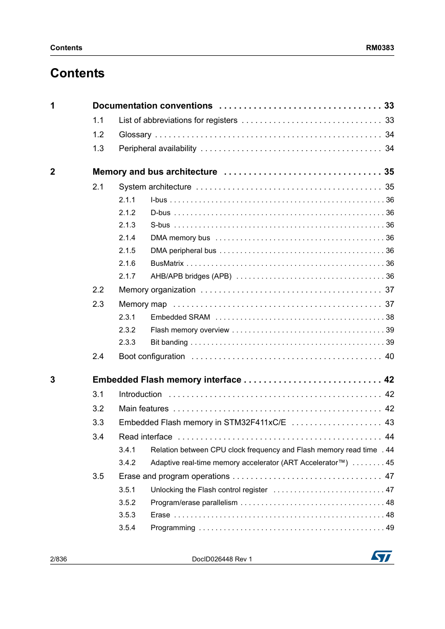
1 Documentation conventions
1.1 List of abbreviations for registers
1.2 Glossary
1.3 Peripheral availability
2 Memory and bus architecture
2.1 System architecture
2.1.1 I-bus
2.1.2 D-bus
2.1.3 S-bus
2.1.4 DMA memory bus
2.1.5 DMA peripheral bus
2.1.6 BusMatrix
2.1.7 AHB/APB bridges (APB)
2.2 Memory organization
2.3 Memory map
Table 1. STM32F411xC/E register boundary addresses (continued)
2.3.1 Embedded SRAM
2.3.2 Flash memory overview
2.3.3 Bit banding
Example
2.4 Boot configuration
Table 2. Boot modes
Embedded bootloader
Physical remap in STM32F411xC/E
Table 3. Memory mapping vs. Boot mode/physical remap in STM32F411xC/E
3 Embedded Flash memory interface
3.1 Introduction
3.2 Main features
3.3 Embedded Flash memory in STM32F411xC/E
Table 4. Flash module organization (STM32F411xC/E)
3.4 Read interface
3.4.1 Relation between CPU clock frequency and Flash memory read time
Table 5. Number of wait states according to CPU clock (HCLK) frequency
Increasing the CPU frequency
Decreasing the CPU frequency
3.4.2 Adaptive real-time memory accelerator (ART Accelerator™)
Instruction prefetch
Instruction cache memory
Data management
3.5 Erase and program operations
3.5.1 Unlocking the Flash control register
3.5.2 Program/erase parallelism
Table 6. Program/erase parallelism
3.5.3 Erase
Sector Erase
Mass Erase
3.5.4 Programming
Standard programming
Programming errors
Programming and caches
3.5.5 Interrupts
Table 7. Flash interrupt request
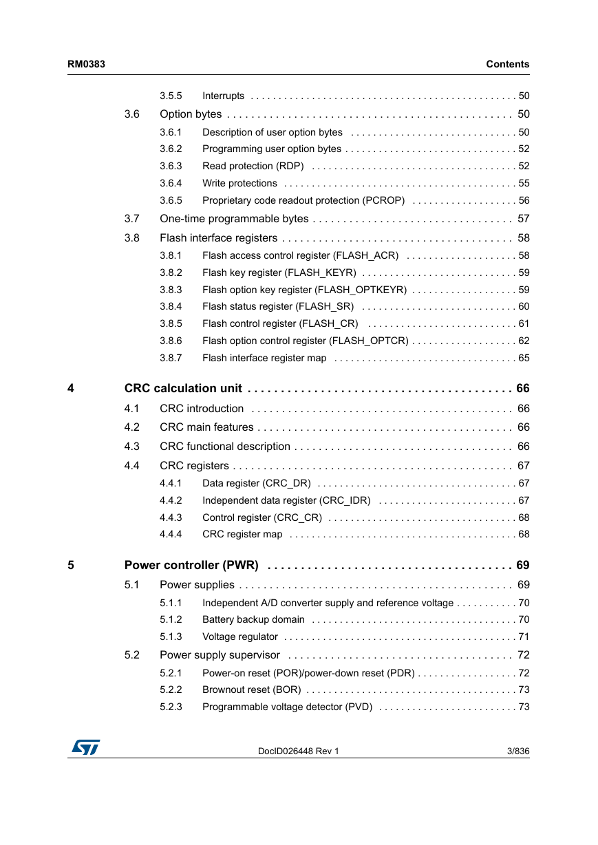
3.6 Option bytes
3.6.1 Description of user option bytes
Table 8. Option byte organization
Table 9. Description of the option bytes (continued)
3.6.2 Programming user option bytes
Modifying user option bytes
3.6.3 Read protection (RDP)
Table 10. Access versus read protection level
3.6.4 Write protections
Write protection error flag
3.6.5 Proprietary code readout protection (PCROP)
3.7 One-time programmable bytes
Table 11. OTP area organization (continued)
3.8 Flash interface registers
3.8.1 Flash access control register (FLASH_ACR)
3.8.2 Flash key register (FLASH_KEYR)
3.8.3 Flash option key register (FLASH_OPTKEYR)
3.8.4 Flash status register (FLASH_SR)
3.8.5 Flash control register (FLASH_CR)
3.8.6 Flash option control register (FLASH_OPTCR)
3.8.7 Flash interface register map
Table 12. Flash register map and reset values
4 CRC calculation unit
4.1 CRC introduction
4.2 CRC main features
4.3 CRC functional description
4.4 CRC registers
4.4.1 Data register (CRC_DR)
4.4.2 Independent data register (CRC_IDR)
4.4.3 Control register (CRC_CR)
4.4.4 CRC register map
Table 13. CRC calculation unit register map and reset values
5 Power controller (PWR)
5.1 Power supplies
5.1.1 Independent A/D converter supply and reference voltage
5.1.2 Battery backup domain
Backup domain description
Backup domain access
RTC and RTC backup registers
5.1.3 Voltage regulator
5.2 Power supply supervisor
5.2.1 Power-on reset (POR)/power-down reset (PDR)
5.2.2 Brownout reset (BOR)
5.2.3 Programmable voltage detector (PVD)
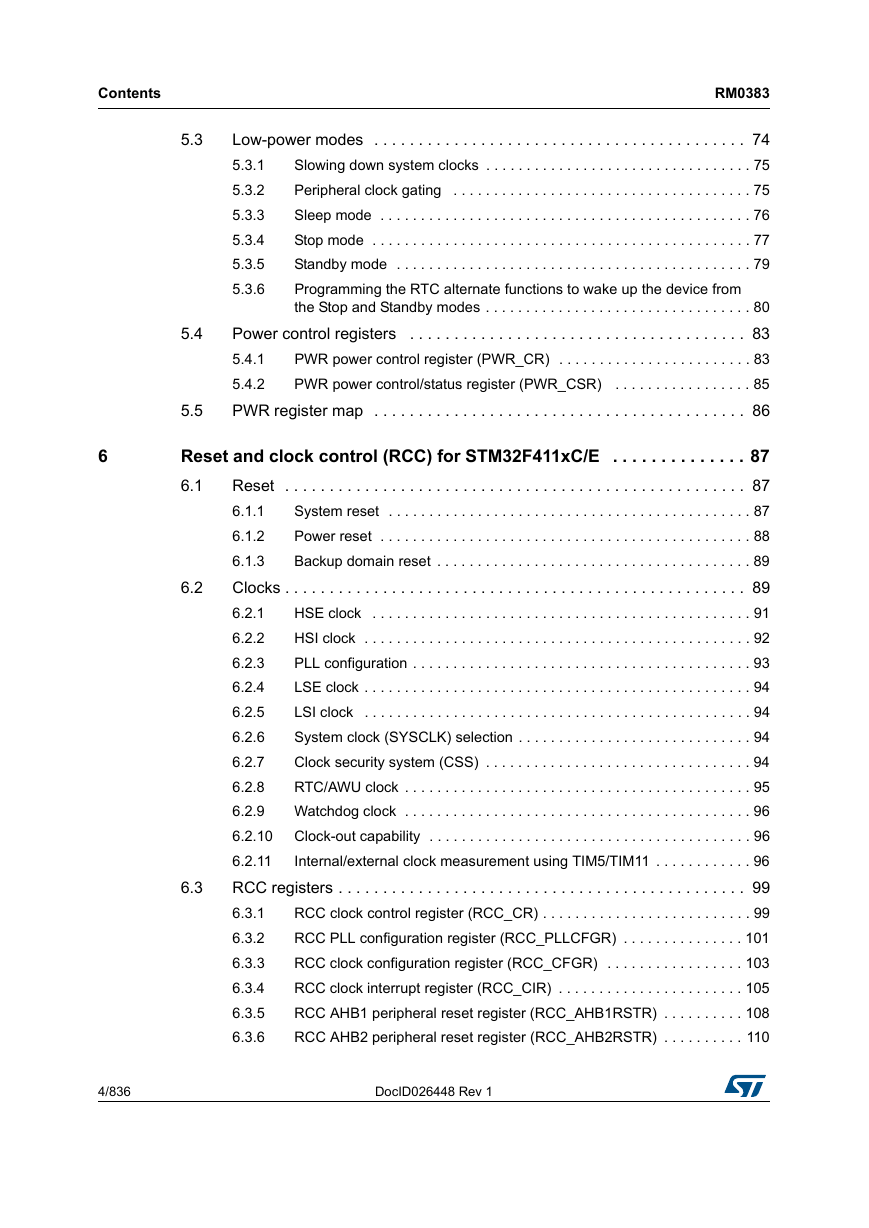
5.3 Low-power modes
Table 14. Low-power mode summary
5.3.1 Slowing down system clocks
5.3.2 Peripheral clock gating
5.3.3 Sleep mode
Entering Sleep mode
Exiting Sleep mode
Table 15. Sleep-now entry and exit
Table 16. Sleep-on-exit entry and exit
5.3.4 Stop mode
Table 17. Stop operating modes
Entering Stop mode
Table 18. Stop mode entry and exit
5.3.5 Standby mode
Entering Standby mode
Exiting Standby mode
Table 19. Standby mode entry and exit
I/O states in Standby mode
Debug mode
5.3.6 Programming the RTC alternate functions to wake up the device from the Stop and Standby modes
RTC alternate functions to wake up the device from the Stop mode
RTC alternate functions to wake up the device from the Standby mode
Safe RTC alternate function wakeup flag clearing sequence
5.4 Power control registers
5.4.1 PWR power control register (PWR_CR)
5.4.2 PWR power control/status register (PWR_CSR)
5.5 PWR register map
Table 20. PWR - register map and reset values
6 Reset and clock control (RCC) for STM32F411xC/E
6.1 Reset
6.1.1 System reset
Software reset
Low-power management reset
6.1.2 Power reset
6.1.3 Backup domain reset
6.2 Clocks
6.2.1 HSE clock
External source (HSE bypass)
External crystal/ceramic resonator (HSE crystal)
6.2.2 HSI clock
Calibration
6.2.3 PLL configuration
6.2.4 LSE clock
External source (LSE bypass)
6.2.5 LSI clock
6.2.6 System clock (SYSCLK) selection
6.2.7 Clock security system (CSS)
6.2.8 RTC/AWU clock
6.2.9 Watchdog clock
6.2.10 Clock-out capability
6.2.11 Internal/external clock measurement using TIM5/TIM11
Internal/external clock measurement using TIM5 channel4
Internal/external clock measurement using TIM11 channel1
6.3 RCC registers
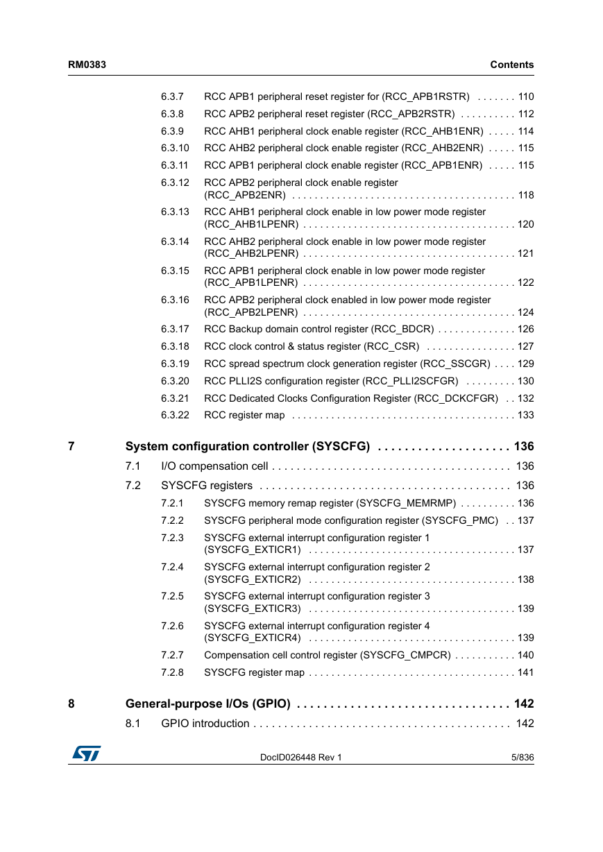
6.3.1 RCC clock control register (RCC_CR)
6.3.2 RCC PLL configuration register (RCC_PLLCFGR)
6.3.3 RCC clock configuration register (RCC_CFGR)
6.3.4 RCC clock interrupt register (RCC_CIR)
6.3.5 RCC AHB1 peripheral reset register (RCC_AHB1RSTR)
6.3.6 RCC AHB2 peripheral reset register (RCC_AHB2RSTR)
6.3.7 RCC APB1 peripheral reset register for (RCC_APB1RSTR)
6.3.8 RCC APB2 peripheral reset register (RCC_APB2RSTR)
6.3.9 RCC AHB1 peripheral clock enable register (RCC_AHB1ENR)
6.3.10 RCC AHB2 peripheral clock enable register (RCC_AHB2ENR)
6.3.11 RCC APB1 peripheral clock enable register (RCC_APB1ENR)
6.3.12 RCC APB2 peripheral clock enable register (RCC_APB2ENR)
6.3.13 RCC AHB1 peripheral clock enable in low power mode register (RCC_AHB1LPENR)
6.3.14 RCC AHB2 peripheral clock enable in low power mode register (RCC_AHB2LPENR)
6.3.15 RCC APB1 peripheral clock enable in low power mode register (RCC_APB1LPENR)
6.3.16 RCC APB2 peripheral clock enabled in low power mode register (RCC_APB2LPENR)
6.3.17 RCC Backup domain control register (RCC_BDCR)
6.3.18 RCC clock control & status register (RCC_CSR)
6.3.19 RCC spread spectrum clock generation register (RCC_SSCGR)
6.3.20 RCC PLLI2S configuration register (RCC_PLLI2SCFGR)
6.3.21 RCC Dedicated Clocks Configuration Register (RCC_DCKCFGR)
6.3.22 RCC register map
7 System configuration controller (SYSCFG)
7.1 I/O compensation cell
7.2 SYSCFG registers
7.2.1 SYSCFG memory remap register (SYSCFG_MEMRMP)
7.2.2 SYSCFG peripheral mode configuration register (SYSCFG_PMC)
7.2.3 SYSCFG external interrupt configuration register 1 (SYSCFG_EXTICR1)
7.2.4 SYSCFG external interrupt configuration register 2 (SYSCFG_EXTICR2)
7.2.5 SYSCFG external interrupt configuration register 3 (SYSCFG_EXTICR3)
7.2.6 SYSCFG external interrupt configuration register 4 (SYSCFG_EXTICR4)
7.2.7 Compensation cell control register (SYSCFG_CMPCR)
7.2.8 SYSCFG register map
Table 22. SYSCFG register map and reset values
8 General-purpose I/Os (GPIO)
8.1 GPIO introduction
8.2 GPIO main features
8.3 GPIO functional description
Table 23. Port bit configuration table (continued)
8.3.1 General-purpose I/O (GPIO)
8.3.2 I/O pin multiplexer and mapping
Table 24. Flexible SWJ-DP pin assignment
8.3.3 I/O port control registers
8.3.4 I/O port data registers
8.3.5 I/O data bitwise handling
8.3.6 GPIO locking mechanism
8.3.7 I/O alternate function input/output
8.3.8 External interrupt/wakeup lines
8.3.9 Input configuration
8.3.10 Output configuration
8.3.11 Alternate function configuration
8.3.12 Analog configuration
8.3.13 Using the OSC32_IN/OSC32_OUT pins as GPIO PC14/PC15 port pins
8.3.14 Using the OSC_IN/OSC_OUT pins as GPIO PH0/PH1 port pins
8.3.15 Selection of RTC additional functions
Table 25. RTC additional functions
8.4 GPIO registers
8.4.1 GPIO port mode register (GPIOx_MODER) (x = A..E and H)
8.4.2 GPIO port output type register (GPIOx_OTYPER) (x = A..E and H)
8.4.3 GPIO port output speed register (GPIOx_OSPEEDR) (x = A..E and H)
8.4.4 GPIO port pull-up/pull-down register (GPIOx_PUPDR) (x = A..E and H)
8.4.5 GPIO port input data register (GPIOx_IDR) (x = A..E and H)
8.4.6 GPIO port output data register (GPIOx_ODR) (x = A..E and H)
8.4.7 GPIO port bit set/reset register (GPIOx_BSRR) (x = A..E and H)
8.4.8 GPIO port configuration lock register (GPIOx_LCKR) (x = A..E and H)
8.4.9 GPIO alternate function low register (GPIOx_AFRL) (x = A..E and H)
8.4.10 GPIO alternate function high register (GPIOx_AFRH) (x = A..E and H)
8.4.11 GPIO register map
Table 26. GPIO register map and reset values (continued)
9 DMA controller (DMA)
9.1 DMA introduction
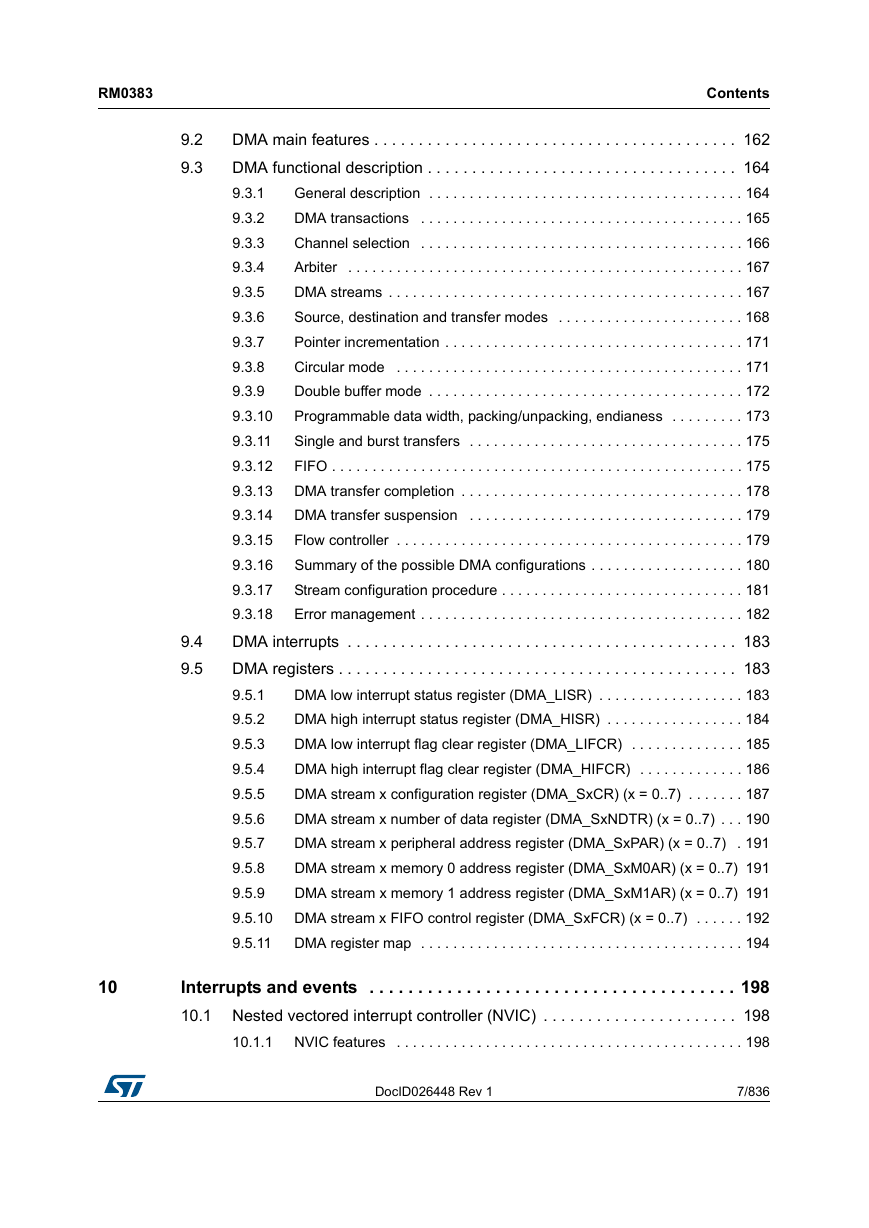
9.2 DMA main features
9.3 DMA functional description
9.3.1 General description
9.3.2 DMA transactions
9.3.3 Channel selection
Table 27. DMA1 request mapping (STM32F411xC/E)
Table 28. DMA2 request mapping (STM32F411xC/E)
9.3.4 Arbiter
9.3.5 DMA streams
9.3.6 Source, destination and transfer modes
Table 29. Source and destination address
Peripheral-to-memory mode
Memory-to-peripheral mode
Memory-to-memory mode
9.3.7 Pointer incrementation
9.3.8 Circular mode
9.3.9 Double buffer mode
Table 30. Source and destination address registers in Double buffer mode (DBM=1)
9.3.10 Programmable data width, packing/unpacking, endianess
Table 31. Packing/unpacking & endian behavior (bit PINC = MINC = 1)
Table 32. Restriction on NDT versus PSIZE and MSIZE
9.3.11 Single and burst transfers
9.3.12 FIFO
FIFO structure
FIFO threshold and burst configuration
Table 33. FIFO threshold configurations (continued)
FIFO flush
Direct mode
9.3.13 DMA transfer completion
9.3.14 DMA transfer suspension
9.3.15 Flow controller
9.3.16 Summary of the possible DMA configurations
Table 34. Possible DMA configurations
9.3.17 Stream configuration procedure
9.3.18 Error management
9.4 DMA interrupts
Table 35. DMA interrupt requests
9.5 DMA registers
9.5.1 DMA low interrupt status register (DMA_LISR)
9.5.2 DMA high interrupt status register (DMA_HISR)
9.5.3 DMA low interrupt flag clear register (DMA_LIFCR)
9.5.4 DMA high interrupt flag clear register (DMA_HIFCR)
9.5.5 DMA stream x configuration register (DMA_SxCR) (x = 0..7)
9.5.6 DMA stream x number of data register (DMA_SxNDTR) (x = 0..7)
9.5.7 DMA stream x peripheral address register (DMA_SxPAR) (x = 0..7)
9.5.8 DMA stream x memory 0 address register (DMA_SxM0AR) (x = 0..7)
9.5.9 DMA stream x memory 1 address register (DMA_SxM1AR) (x = 0..7)
9.5.10 DMA stream x FIFO control register (DMA_SxFCR) (x = 0..7)
9.5.11 DMA register map
Table 36. DMA register map and reset values (continued)
10 Interrupts and events
10.1 Nested vectored interrupt controller (NVIC)
10.1.1 NVIC features
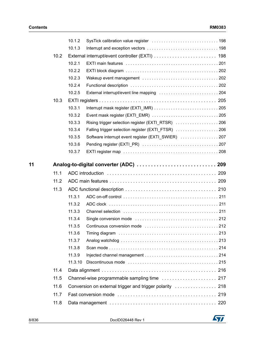
10.1.2 SysTick calibration value register
10.1.3 Interrupt and exception vectors
10.2 External interrupt/event controller (EXTI)
Table 37. Vector table for STM32F411xC/E (continued)
10.2.1 EXTI main features
10.2.2 EXTI block diagram
10.2.3 Wakeup event management
10.2.4 Functional description
Hardware interrupt selection
Hardware event selection
Software interrupt/event selection
10.2.5 External interrupt/event line mapping
10.3 EXTI registers
10.3.1 Interrupt mask register (EXTI_IMR)
10.3.2 Event mask register (EXTI_EMR)
10.3.3 Rising trigger selection register (EXTI_RTSR)
10.3.4 Falling trigger selection register (EXTI_FTSR)
10.3.5 Software interrupt event register (EXTI_SWIER)
10.3.6 Pending register (EXTI_PR)
10.3.7 EXTI register map
Table 38. External interrupt/event controller register map and reset values
11 Analog-to-digital converter (ADC)
11.1 ADC introduction
11.2 ADC main features
11.3 ADC functional description
Table 39. ADC pins
11.3.1 ADC on-off control
11.3.2 ADC clock
11.3.3 Channel selection
Temperature sensor, VREFINT and VBAT internal channels
11.3.4 Single conversion mode
11.3.5 Continuous conversion mode
11.3.6 Timing diagram
11.3.7 Analog watchdog
Table 40. Analog watchdog channel selection
11.3.8 Scan mode
11.3.9 Injected channel management
Triggered injection
Auto-injection
11.3.10 Discontinuous mode
Regular group
Injected group
11.4 Data alignment
11.5 Channel-wise programmable sampling time
11.6 Conversion on external trigger and trigger polarity
Table 41. Configuring the trigger polarity
Table 42. External trigger for regular channels
Table 43. External trigger for injected channels
11.7 Fast conversion mode
11.8 Data management
11.8.1 Using the DMA
11.8.2 Managing a sequence of conversions without using the DMA
11.8.3 Conversions without DMA and without overrun detection
11.9 Temperature sensor
Main features
Reading the temperature
11.10 Battery charge monitoring
11.11 ADC interrupts
Table 44. ADC interrupts
11.12 ADC registers
11.12.1 ADC status register (ADC_SR)
11.12.2 ADC control register 1 (ADC_CR1)
11.12.3 ADC control register 2 (ADC_CR2)
11.12.4 ADC sample time register 1 (ADC_SMPR1)
11.12.5 ADC sample time register 2 (ADC_SMPR2)
11.12.6 ADC injected channel data offset register x (ADC_JOFRx) (x=1..4)
11.12.7 ADC watchdog higher threshold register (ADC_HTR)
11.12.8 ADC watchdog lower threshold register (ADC_LTR)
11.12.9 ADC regular sequence register 1 (ADC_SQR1)
11.12.10 ADC regular sequence register 2 (ADC_SQR2)
11.12.11 ADC regular sequence register 3 (ADC_SQR3)
11.12.12 ADC injected sequence register (ADC_JSQR)
11.12.13 ADC injected data register x (ADC_JDRx) (x= 1..4)
11.12.14 ADC regular data register (ADC_DR)
11.12.15 ADC common control register (ADC_CCR)
11.12.16 ADC register map
Table 45. ADC global register map
Table 46. ADC register map and reset values for each ADC
Table 47. ADC register map and reset values (common ADC registers)
12 Advanced-control timer (TIM1)
12.1 TIM1 introduction
12.2 TIM1 main features
12.3 TIM1 functional description
12.3.1 Time-base unit
Prescaler description
12.3.2 Counter modes
Upcounting mode
Downcounting mode
Center-aligned mode (up/down counting)
12.3.3 Repetition counter
12.3.4 Clock selection
Internal clock source (CK_INT)
External clock source mode 1
External clock source mode 2
12.3.5 Capture/compare channels
12.3.6 Input capture mode
12.3.7 PWM input mode
12.3.8 Forced output mode
12.3.9 Output compare mode
12.3.10 PWM mode
PWM edge-aligned mode
PWM center-aligned mode
12.3.11 Complementary outputs and dead-time insertion
Re-directing OCxREF to OCx or OCxN
12.3.12 Using the break function
12.3.13 Clearing the OCxREF signal on an external event
12.3.14 6-step PWM generation
12.3.15 One-pulse mode
12.3.16 Encoder interface mode
Table 48. Counting direction versus encoder signals
12.3.17 Timer input XOR function
12.3.18 Interfacing with Hall sensors
12.3.19 TIMx and external trigger synchronization
Slave mode: Reset mode
Slave mode: Gated mode
Slave mode: Trigger mode
Slave mode: external clock mode 2 + trigger mode
12.3.20 Timer synchronization
12.3.21 Debug mode
12.4 TIM1 registers
12.4.1 TIM1 control register 1 (TIMx_CR1)
12.4.2 TIM1 control register 2 (TIMx_CR2)
12.4.3 TIM1 slave mode control register (TIMx_SMCR)
Table 49. TIMx Internal trigger connection
12.4.4 TIM1 DMA/interrupt enable register (TIMx_DIER)
12.4.5 TIM1 status register (TIMx_SR)
12.4.6 TIM1 event generation register (TIMx_EGR)
12.4.7 TIM1 capture/compare mode register 1 (TIMx_CCMR1)
Output compare mode:
Input capture mode
12.4.8 TIM1 capture/compare mode register 2 (TIMx_CCMR2)
Output compare mode
Input capture mode
12.4.9 TIM1 capture/compare enable register (TIMx_CCER)
Table 50. Output control bits for complementary OCx and OCxN channels with break feature
12.4.10 TIM1 counter (TIMx_CNT)
12.4.11 TIM1 prescaler (TIMx_PSC)
12.4.12 TIM1 auto-reload register (TIMx_ARR)
12.4.13 TIM1 repetition counter register (TIMx_RCR)
12.4.14 TIM1 capture/compare register 1 (TIMx_CCR1)
12.4.15 TIM1 capture/compare register 2 (TIMx_CCR2)
12.4.16 TIM1 capture/compare register 3 (TIMx_CCR3)
12.4.17 TIM1 capture/compare register 4 (TIMx_CCR4)
12.4.18 TIM1 break and dead-time register (TIMx_BDTR)
12.4.19 TIM1 DMA control register (TIMx_DCR)
12.4.20 TIM1 DMA address for full transfer (TIMx_DMAR)
Example of how to use the DMA burst feature
12.4.21 TIM1 register map
Table 51. TIM1 register map and reset values (continued)
13 General-purpose timers (TIM2 to TIM5)
13.1 TIM2 to TIM5 introduction
13.2 TIM2 to TIM5 main features
13.3 TIM2 to TIM5 functional description
13.3.1 Time-base unit
13.3.2 Counter modes
13.3.3 Clock selection
13.3.4 Capture/compare channels
13.3.5 Input capture mode
13.3.6 PWM input mode
13.3.7 Forced output mode
13.3.8 Output compare mode
13.3.9 PWM mode
13.3.10 One-pulse mode
13.3.11 Clearing the OCxREF signal on an external event
13.3.12 Encoder interface mode
Table 52. Counting direction versus encoder signals
13.3.13 Timer input XOR function
13.3.14 Timers and external trigger synchronization
13.3.15 Timer synchronization
13.3.16 Debug mode
13.4 TIM2 to TIM5 registers
13.4.1 TIMx control register 1 (TIMx_CR1)
13.4.2 TIMx control register 2 (TIMx_CR2)
13.4.3 TIMx slave mode control register (TIMx_SMCR)
Table 53. TIMx internal trigger connection
13.4.4 TIMx DMA/Interrupt enable register (TIMx_DIER)
13.4.5 TIMx status register (TIMx_SR)
13.4.6 TIMx event generation register (TIMx_EGR)
13.4.7 TIMx capture/compare mode register 1 (TIMx_CCMR1)
13.4.8 TIMx capture/compare mode register 2 (TIMx_CCMR2)
13.4.9 TIMx capture/compare enable register (TIMx_CCER)
Table 54. Output control bit for standard OCx channels
13.4.10 TIMx counter (TIMx_CNT)
13.4.11 TIMx prescaler (TIMx_PSC)
13.4.12 TIMx auto-reload register (TIMx_ARR)
13.4.13 TIMx capture/compare register 1 (TIMx_CCR1)
13.4.14 TIMx capture/compare register 2 (TIMx_CCR2)
13.4.15 TIMx capture/compare register 3 (TIMx_CCR3)
13.4.16 TIMx capture/compare register 4 (TIMx_CCR4)
13.4.17 TIMx DMA control register (TIMx_DCR)
13.4.18 TIMx DMA address for full transfer (TIMx_DMAR)
13.4.19 TIM2 option register (TIM2_OR)
13.4.20 TIM5 option register (TIM5_OR)
13.4.21 TIMx register map
Table 55. TIM2 to TIM5 register map and reset values (continued)
14 General-purpose timers (TIM9 to TIM11)
14.1 TIM9/10/11 introduction
14.2 TIM9/10/11 main features
14.2.1 TIM9 main features
14.2.2 TIM10/TIM11 main features
14.3 TIM9 to TIM11 functional description
14.3.1 Time-base unit
14.3.2 Counter modes
14.3.3 Clock selection
14.3.4 Capture/compare channels
14.3.5 Input capture mode
14.3.6 PWM input mode (only for TIM9)
14.3.7 Forced output mode
14.3.8 Output compare mode
14.3.9 PWM mode
14.3.10 One-pulse mode
14.3.11 TIM9 external trigger synchronization
14.3.12 Timer synchronization (TIM9)
14.3.13 Debug mode
14.4 TIM9 registers
14.4.1 TIM9 control register 1 (TIMx_CR1)
14.4.2 TIM9 slave mode control register (TIMx_SMCR)
Table 56. TIMx internal trigger connection
14.4.3 TIM9 Interrupt enable register (TIMx_DIER)
14.4.4 TIM9 status register (TIMx_SR)
14.4.5 TIM9 event generation register (TIMx_EGR)
14.4.6 TIM9 capture/compare mode register 1 (TIMx_CCMR1)
14.4.7 TIM9 capture/compare enable register (TIMx_CCER)
Table 57. Output control bit for standard OCx channels
14.4.8 TIM9 counter (TIMx_CNT)
14.4.9 TIM9 prescaler (TIMx_PSC)
14.4.10 TIM9 auto-reload register (TIMx_ARR)
14.4.11 TIM9 capture/compare register 1 (TIMx_CCR1)
14.4.12 TIM9 capture/compare register 2 (TIMx_CCR2)
14.4.13 TIM9 register map
Table 58. TIM9 register map and reset values (continued)
14.5 TIM10/11 registers
14.5.1 TIM10/11 control register 1 (TIMx_CR1)
14.5.2 TIM status register (TIMx_SR)
14.5.3 TIM event generation register (TIMx_EGR)
14.5.4 TIM10/11 capture/compare mode register 1 (TIMx_CCMR1)
14.5.5 TIM10/11 capture/compare enable register (TIMx_CCER)
Table 59. Output control bit for standard OCx channels
14.5.6 TIM10/11 counter (TIMx_CNT)
14.5.7 TIM10/11 prescaler (TIMx_PSC)
14.5.8 TIM10/11 auto-reload register (TIMx_ARR)
14.5.9 TIM10/11 capture/compare register 1 (TIMx_CCR1)
14.5.10 TIM11 option register 1 (TIM11_OR)
14.5.11 TIM10/11 register map
Table 60. TIM10/11 register map and reset values (continued)
15 Independent watchdog (IWDG)
15.1 IWDG introduction
15.2 IWDG main features
15.3 IWDG functional description
15.3.1 Hardware watchdog
15.3.2 Register access protection
15.3.3 Debug mode
Table 61. Min/max IWDG timeout period at 32 kHz (LSI)
15.4 IWDG registers
15.4.1 Key register (IWDG_KR)
15.4.2 Prescaler register (IWDG_PR)
15.4.3 Reload register (IWDG_RLR)
15.4.4 Status register (IWDG_SR)
15.4.5 IWDG register map
Table 62. IWDG register map and reset values
16 Window watchdog (WWDG)
16.1 WWDG introduction
16.2 WWDG main features
16.3 WWDG functional description
16.4 How to program the watchdog timeout
16.5 Debug mode
16.6 WWDG registers
16.6.1 Control register (WWDG_CR)
16.6.2 Configuration register (WWDG_CFR)
16.6.3 Status register (WWDG_SR)
16.6.4 WWDG register map
Table 63. WWDG register map and reset values
17 Real-time clock (RTC)
17.1 Introduction
17.2 RTC main features
17.3 RTC functional description
17.3.1 Clock and prescalers
17.3.2 Real-time clock and calendar
17.3.3 Programmable alarms
17.3.4 Periodic auto-wakeup
17.3.5 RTC initialization and configuration
17.3.6 Reading the calendar
17.3.7 Resetting the RTC
17.3.8 RTC synchronization
17.3.9 RTC reference clock detection
17.3.10 RTC coarse digital calibration
17.3.11 RTC smooth digital calibration
17.3.12 Timestamp function
17.3.13 Tamper detection
17.3.14 Calibration clock output
17.3.15 Alarm output
17.4 RTC and low power modes
Table 64. Effect of low power modes on RTC
17.5 RTC interrupts
Table 65. Interrupt control bits
17.6 RTC registers
17.6.1 RTC time register (RTC_TR)
17.6.2 RTC date register (RTC_DR)
17.6.3 RTC control register (RTC_CR)
17.6.4 RTC initialization and status register (RTC_ISR)
17.6.5 RTC prescaler register (RTC_PRER)
17.6.6 RTC wakeup timer register (RTC_WUTR)
17.6.7 RTC calibration register (RTC_CALIBR)
17.6.8 RTC alarm A register (RTC_ALRMAR)
17.6.9 RTC alarm B register (RTC_ALRMBR)
17.6.10 RTC write protection register (RTC_WPR)
17.6.11 RTC sub second register (RTC_SSR)
17.6.12 RTC shift control register (RTC_SHIFTR)
17.6.13 RTC time stamp time register (RTC_TSTR)
17.6.14 RTC time stamp date register (RTC_TSDR)
17.6.15 RTC timestamp sub second register (RTC_TSSSR)
17.6.16 RTC calibration register (RTC_CALR)
17.6.17 RTC tamper and alternate function configuration register (RTC_TAFCR)
17.6.18 RTC alarm A sub second register (RTC_ALRMASSR)
17.6.19 RTC alarm B sub second register (RTC_ALRMBSSR)
17.6.20 RTC backup registers (RTC_BKPxR)
17.6.21 RTC register map
Table 66. RTC register map and reset values (continued)
18 Inter-integrated circuit (I2C) interface
18.1 I2C introduction
18.2 I2C main features
18.3 I2C functional description
18.3.1 Mode selection
18.3.2 I2C slave mode
18.3.3 I2C master mode
18.3.4 Error conditions
18.3.5 Programmable noise filter
Table 67. Maximum DNF[3:0] value to be compliant with Thd:dat(max)
18.3.6 SDA/SCL line control
18.3.7 SMBus
Table 68. SMBus vs. I2C
18.3.8 DMA requests
18.3.9 Packet error checking
18.4 I2C interrupts
Table 69. I2C Interrupt requests
18.5 I2C debug mode
18.6 I2C registers
18.6.1 I2C Control register 1 (I2C_CR1)
18.6.2 I2C Control register 2 (I2C_CR2)
18.6.3 I2C Own address register 1 (I2C_OAR1)
18.6.4 I2C Own address register 2 (I2C_OAR2)
18.6.5 I2C Data register (I2C_DR)
18.6.6 I2C Status register 1 (I2C_SR1)
18.6.7 I2C Status register 2 (I2C_SR2)
18.6.8 I2C Clock control register (I2C_CCR)
18.6.9 I2C TRISE register (I2C_TRISE)
18.6.10 I2C FLTR register (I2C_FLTR)
18.6.11 I2C register map
Table 70. I2C register map and reset values (continued)
19 Universal synchronous asynchronous receiver transmitter (USART)
19.1 USART introduction
19.2 USART main features
19.3 USART functional description
19.3.1 USART character description
19.3.2 Transmitter
19.3.3 Receiver
Table 71. Noise detection from sampled data (continued)
19.3.4 Fractional baud rate generation
Table 72. Error calculation for programmed baud rates at fPCLK = 8 MHz or fPCLK = 12 MHz, oversampling by 16 (continued)
Table 73. Error calculation for programmed baud rates at fPCLK = 8 MHz or fPCLK =12 MHz, oversampling by 8 (continued)
Table 74. Error calculation for programmed baud rates at fPCLK = 16 MHz or fPCLK = 24 MHz, oversampling by 16
Table 75. Error calculation for programmed baud rates at fPCLK = 16 MHz or fPCLK = 24 MHz, oversampling by 8
Table 76. Error calculation for programmed baud rates at fPCLK = 8 MHz or fPCLK = 16 MHz, oversampling by 16 (continued)
Table 77. Error calculation for programmed baud rates at fPCLK = 8 MHz or fPCLK = 16 MHz, oversampling by 8 (continued)
Table 78. Error calculation for programmed baud rates at fPCLK = 30 MHz or fPCLK = 60 MHz, oversampling by 16 (continued)
Table 79. Error calculation for programmed baud rates at fPCLK = 30 MHz or fPCLK = 60 MHz, oversampling by 8
Table 80. Error calculation for programmed baud rates at fPCLK = 42 MHz or fPCLK = 84 Hz, oversampling by 16
Table 81. Error calculation for programmed baud rates at fPCLK = 42 MHz or fPCLK = 84 MHz, oversampling by 8
19.3.5 USART receiver tolerance to clock deviation
Table 82. USART receiver’s tolerance when DIV fraction is 0
Table 83. USART receiver tolerance when DIV_Fraction is different from 0
19.3.6 Multiprocessor communication
19.3.7 Parity control
Table 84. Frame formats
19.3.8 LIN (local interconnection network) mode
19.3.9 USART synchronous mode
19.3.10 Single-wire half-duplex communication
19.3.11 Smartcard
19.3.12 IrDA SIR ENDEC block
19.3.13 Continuous communication using DMA
19.3.14 Hardware flow control
19.4 USART interrupts
Table 85. USART interrupt requests
19.5 USART mode configuration
Table 86. USART mode configuration
19.6 USART registers
19.6.1 Status register (USART_SR)
19.6.2 Data register (USART_DR)
19.6.3 Baud rate register (USART_BRR)
19.6.4 Control register 1 (USART_CR1)
19.6.5 Control register 2 (USART_CR2)
19.6.6 Control register 3 (USART_CR3)
19.6.7 Guard time and prescaler register (USART_GTPR)
19.6.8 USART register map
Table 87. USART register map and reset values
20 Serial peripheral interface (SPI)
20.1 SPI introduction
20.2 SPI and I2S main features
20.2.1 SPI features
20.2.2 I2S features
20.3 SPI functional description
20.3.1 General description
20.3.2 Configuring the SPI in slave mode
20.3.3 Configuring the SPI in master mode
20.3.4 Configuring the SPI for half-duplex communication
20.3.5 Data transmission and reception procedures
20.3.6 CRC calculation
20.3.7 Status flags
20.3.8 Disabling the SPI
20.3.9 SPI communication using DMA (direct memory addressing)
20.3.10 Error flags
20.3.11 SPI interrupts
Table 88. SPI interrupt requests
20.4 I2S functional description
20.4.1 I2S general description
20.4.2 I2S full duplex
20.4.3 Supported audio protocols
20.4.4 Clock generator
Table 89. Audio frequency precision (for PLLM VCO = 1 MHz or 2 MHz)
20.4.5 I2S master mode
20.4.6 I2S slave mode
20.4.7 Status flags
20.4.8 Error flags
20.4.9 I2S interrupts
Table 90. I2S interrupt requests
20.4.10 DMA features
20.5 SPI and I2S registers
20.5.1 SPI control register 1 (SPI_CR1)(not used in I2S mode)
20.5.2 SPI control register 2 (SPI_CR2)
20.5.3 SPI status register (SPI_SR)
20.5.4 SPI data register (SPI_DR)
20.5.5 SPI CRC polynomial register (SPI_CRCPR)(not used in I2S mode)
20.5.6 SPI RX CRC register (SPI_RXCRCR)(not used in I2S mode)
20.5.7 SPI TX CRC register (SPI_TXCRCR)(not used in I2S mode)
20.5.8 SPI_I2S configuration register (SPI_I2SCFGR)
20.5.9 SPI_I2S prescaler register (SPI_I2SPR)
20.5.10 SPI register map
Table 91. SPI register map and reset values
21 Secure digital input/output interface (SDIO)
21.1 SDIO main features
21.2 SDIO bus topology
21.3 SDIO functional description
Table 92. SDIO I/O definitions
21.3.1 SDIO adapter
Table 93. Command format
Table 94. Short response format
Table 95. Long response format
Table 96. Command path status flags
Table 97. Data token format
Table 98. Transmit FIFO status flags
Table 99. Receive FIFO status flags
21.3.2 SDIO APB2 interface
21.4 Card functional description
21.4.1 Card identification mode
21.4.2 Card reset
21.4.3 Operating voltage range validation
21.4.4 Card identification process
21.4.5 Block write
21.4.6 Block read
21.4.7 Stream access, stream write and stream read (MultiMediaCard only)
21.4.8 Erase: group erase and sector erase
21.4.9 Wide bus selection or deselection
21.4.10 Protection management
21.4.11 Card status register
Table 100. Card status (continued)
21.4.12 SD status register
Table 101. SD status
Table 102. Speed class code field
Table 103. Performance move field
Table 104. AU_SIZE field
Table 105. Maximum AU size
Table 106. Erase size field
Table 107. Erase timeout field
Table 108. Erase offset field
21.4.13 SD I/O mode
21.4.14 Commands and responses
Table 109. Block-oriented write commands (continued)
Table 110. Block-oriented write protection commands
Table 111. Erase commands
Table 112. I/O mode commands
Table 113. Lock card
Table 114. Application-specific commands
21.5 Response formats
21.5.1 R1 (normal response command)
Table 115. R1 response
21.5.2 R1b
21.5.3 R2 (CID, CSD register)
Table 116. R2 response
21.5.4 R3 (OCR register)
Table 117. R3 response
21.5.5 R4 (Fast I/O)
Table 118. R4 response
21.5.6 R4b
Table 119. R4b response
21.5.7 R5 (interrupt request)
Table 120. R5 response
21.5.8 R6
Table 121. R6 response
21.6 SDIO I/O card-specific operations
21.6.1 SDIO I/O read wait operation by SDIO_D2 signalling
21.6.2 SDIO read wait operation by stopping SDIO_CK
21.6.3 SDIO suspend/resume operation
21.6.4 SDIO interrupts
21.7 CE-ATA specific operations
21.7.1 Command completion signal disable
21.7.2 Command completion signal enable
21.7.3 CE-ATA interrupt
21.7.4 Aborting CMD61
21.8 HW flow control
21.9 SDIO registers
21.9.1 SDIO power control register (SDIO_POWER)
21.9.2 SDI clock control register (SDIO_CLKCR)
21.9.3 SDIO argument register (SDIO_ARG)
21.9.4 SDIO command register (SDIO_CMD)
21.9.5 SDIO command response register (SDIO_RESPCMD)
21.9.6 SDIO response 1..4 register (SDIO_RESPx)
Table 122. Response type and SDIO_RESPx registers
21.9.7 SDIO data timer register (SDIO_DTIMER)
21.9.8 SDIO data length register (SDIO_DLEN)
21.9.9 SDIO data control register (SDIO_DCTRL)
21.9.10 SDIO data counter register (SDIO_DCOUNT)
21.9.11 SDIO status register (SDIO_STA)
21.9.12 SDIO interrupt clear register (SDIO_ICR)
21.9.13 SDIO mask register (SDIO_MASK)
21.9.14 SDIO FIFO counter register (SDIO_FIFOCNT)
21.9.15 SDIO data FIFO register (SDIO_FIFO)
21.9.16 SDIO register map
Table 123. SDIO register map (continued)
22 USB on-the-go full-speed (OTG_FS)
22.1 OTG_FS introduction
22.2 OTG_FS main features
22.2.1 General features
22.2.2 Host-mode features
22.2.3 Peripheral-mode features
22.3 OTG_FS functional description
22.3.1 OTG full-speed core
22.3.2 Full-speed OTG PHY
22.4 OTG dual role device (DRD)
22.4.1 ID line detection
22.4.2 HNP dual role device
22.4.3 SRP dual role device
22.5 USB peripheral
22.5.1 SRP-capable peripheral
22.5.2 Peripheral states
Powered state
Soft disconnect
Default state
Suspended state
22.5.3 Peripheral endpoints
Endpoint control
Endpoint transfer
Endpoint status/interrupt
22.6 USB host
22.6.1 SRP-capable host
22.6.2 USB host states
Host port power
VBUS valid
Host detection of a peripheral connection
Host detection of peripheral a disconnection
Host enumeration
Host suspend
22.6.3 Host channels
Host channel control
Host channel transfer
Host channel status/interrupt
22.6.4 Host scheduler
22.7 SOF trigger
22.7.1 Host SOFs
22.7.2 Peripheral SOFs
22.8 Power options
22.9 Dynamic update of the OTG_FS_HFIR register
22.10 USB data FIFOs
22.11 Peripheral FIFO architecture
22.11.1 Peripheral Rx FIFO
22.11.2 Peripheral Tx FIFOs
22.12 Host FIFO architecture
22.12.1 Host Rx FIFO
22.12.2 Host Tx FIFOs
22.13 FIFO RAM allocation
22.13.1 Device mode
22.13.2 Host mode
Receive FIFO RAM allocation
Transmit FIFO RAM allocation
22.14 USB system performance
22.15 OTG_FS interrupts
22.16 OTG_FS control and status registers
22.16.1 CSR memory map
Global CSR map
Table 124. Core global control and status registers (CSRs) (continued)
Host-mode CSR map
Table 125. Host-mode control and status registers (CSRs) (continued)
Device-mode CSR map
Table 126. Device-mode control and status registers (continued)
Data FIFO (DFIFO) access register map
Table 127. Data FIFO (DFIFO) access register map
Power and clock gating CSR map
Table 128. Power and clock gating control and status registers
22.16.2 OTG_FS global registers
OTG_FS control and status register (OTG_FS_GOTGCTL)
OTG_FS interrupt register (OTG_FS_GOTGINT)
OTG_FS AHB configuration register (OTG_FS_GAHBCFG)
OTG_FS USB configuration register (OTG_FS_GUSBCFG)
OTG_FS reset register (OTG_FS_GRSTCTL)
OTG_FS core interrupt register (OTG_FS_GINTSTS)
OTG_FS interrupt mask register (OTG_FS_GINTMSK)
OTG_FS Receive status debug read/OTG status read and pop registers (OTG_FS_GRXSTSR/OTG_FS_GRXSTSP)
OTG_FS Receive FIFO size register (OTG_FS_GRXFSIZ)
OTG_FS Host non-periodic transmit FIFO size register (OTG_FS_HNPTXFSIZ)/Endpoint 0 Transmit FIFO size (OTG_FS_DIEPTXF0)
OTG_FS non-periodic transmit FIFO/queue status register (OTG_FS_HNPTXSTS)
OTG_FS general core configuration register (OTG_FS_GCCFG)
OTG_FS core ID register (OTG_FS_CID)
OTG_FS Host periodic transmit FIFO size register (OTG_FS_HPTXFSIZ)
OTG_FS device IN endpoint transmit FIFO size register (OTG_FS_DIEPTXFx) (x = 1..3, where x is the FIFO_number)
22.16.3 Host-mode registers
OTG_FS Host configuration register (OTG_FS_HCFG)
OTG_FS Host frame interval register (OTG_FS_HFIR)
OTG_FS Host frame number/frame time remaining register (OTG_FS_HFNUM)
OTG_FS_Host periodic transmit FIFO/queue status register (OTG_FS_HPTXSTS)
OTG_FS Host all channels interrupt register (OTG_FS_HAINT)
OTG_FS Host all channels interrupt mask register (OTG_FS_HAINTMSK)
OTG_FS Host port control and status register (OTG_FS_HPRT)
OTG_FS Host channel-x characteristics register (OTG_FS_HCCHARx) (x = 0..7, where x = Channel_number)
OTG_FS Host channel-x interrupt register (OTG_FS_HCINTx) (x = 0..7, where x = Channel_number)
OTG_FS Host channel-x interrupt mask register (OTG_FS_HCINTMSKx) (x = 0..7, where x = Channel_number)
OTG_FS Host channel-x transfer size register (OTG_FS_HCTSIZx) (x = 0..7, where x = Channel_number)
22.16.4 Device-mode registers
OTG_FS device configuration register (OTG_FS_DCFG)
OTG_FS device control register (OTG_FS_DCTL)
Table 129. Minimum duration for soft disconnect
OTG_FS device status register (OTG_FS_DSTS)
OTG_FS device IN endpoint common interrupt mask register (OTG_FS_DIEPMSK)
OTG_FS device OUT endpoint common interrupt mask register (OTG_FS_DOEPMSK)
OTG_FS device all endpoints interrupt register (OTG_FS_DAINT)
OTG_FS all endpoints interrupt mask register (OTG_FS_DAINTMSK)
OTG_FS device VBUS discharge time register (OTG_FS_DVBUSDIS)
OTG_FS device VBUS pulsing time register (OTG_FS_DVBUSPULSE)
OTG_FS device IN endpoint FIFO empty interrupt mask register: (OTG_FS_DIEPEMPMSK)
OTG_FS device control IN endpoint 0 control register (OTG_FS_DIEPCTL0)
OTG device endpoint-x control register (OTG_FS_DIEPCTLx) (x = 1..3, where x = Endpoint_number)
OTG_FS device control OUT endpoint 0 control register (OTG_FS_DOEPCTL0)
OTG_FS device endpoint-x control register (OTG_FS_DOEPCTLx) (x = 1..3, where x = Endpoint_number)
OTG_FS device endpoint-x interrupt register (OTG_FS_DIEPINTx) (x = 0..3, where x = Endpoint_number)
OTG_FS device endpoint-x interrupt register (OTG_FS_DOEPINTx) (x = 0..3, where x = Endpoint_number)
OTG_FS device IN endpoint 0 transfer size register (OTG_FS_DIEPTSIZ0)
OTG_FS device OUT endpoint 0 transfer size register (OTG_FS_DOEPTSIZ0)
OTG_FS device endpoint-x transfer size register (OTG_FS_DIEPTSIZx) (x = 1..3, where x = Endpoint_number)
OTG_FS device IN endpoint transmit FIFO status register (OTG_FS_DTXFSTSx) (x = 0..3, where x = Endpoint_number)
OTG_FS device OUT endpoint-x transfer size register (OTG_FS_DOEPTSIZx) (x = 1..3, where x = Endpoint_number)
22.16.5 OTG_FS power and clock gating control register (OTG_FS_PCGCCTL)
22.16.6 OTG_FS register map
Table 130. OTG_FS register map and reset values (continued)
22.17 OTG_FS programming model
22.17.1 Core initialization
22.17.2 Host initialization
22.17.3 Device initialization
22.17.4 Host programming model
Channel initialization
Halting a channel
Operational model
22.17.5 Device programming model
Endpoint initialization on USB reset
Endpoint initialization on enumeration completion
Endpoint initialization on SetAddress command
Endpoint initialization on SetConfiguration/SetInterface command
Endpoint activation
Endpoint deactivation
22.17.6 Operational model
SETUP and OUT data transfers
Examples
IN data transfers
22.17.7 Worst case response time
Choosing the value of TRDT in OTG_FS_GUSBCFG
22.17.8 OTG programming model
A-device session request protocol
B-device session request protocol
A-device host negotiation protocol
B-device host negotiation protocol
23 Debug support (DBG)
23.1 Overview
23.2 Reference ARM® documentation
23.3 SWJ debug port (serial wire and JTAG)
23.3.1 Mechanism to select the JTAG-DP or the SW-DP
23.4 Pinout and debug port pins
23.4.1 SWJ debug port pins
Table 131. SWJ debug port pins
23.4.2 Flexible SWJ-DP pin assignment
Table 132. Flexible SWJ-DP pin assignment
23.4.3 Internal pull-up and pull-down on JTAG pins
23.4.4 Using serial wire and releasing the unused debug pins as GPIOs
23.5 STM32F411xC/E JTAG TAP connection
23.6 ID codes and locking mechanism
23.6.1 MCU device ID code
23.6.2 Boundary scan TAP
23.6.3 Cortex®-M4 with FPU TAP
23.6.4 Cortex®-M4 with FPU JEDEC-106 ID code
23.7 JTAG debug port
Table 133. JTAG debug port data registers (continued)
Table 134. 32-bit debug port registers addressed through the shifted value A[3:2]
23.8 SW debug port
23.8.1 SW protocol introduction
23.8.2 SW protocol sequence
Table 135. Packet request (8-bits)
Table 136. ACK response (3 bits)
Table 137. DATA transfer (33 bits)
23.8.3 SW-DP state machine (reset, idle states, ID code)
23.8.4 DP and AP read/write accesses
23.8.5 SW-DP registers
Table 138. SW-DP registers (continued)
23.8.6 SW-AP registers
23.9 AHB-AP (AHB access port) - valid for both JTAG-DP and SW-DP
Table 139. Cortex®-M4 with FPU AHB-AP registers
23.10 Core debug
Table 140. Core debug registers
23.11 Capability of the debugger host to connect under system reset
23.12 FPB (Flash patch breakpoint)
23.13 DWT (data watchpoint trigger)
23.14 ITM (instrumentation trace macrocell)
23.14.1 General description
23.14.2 Time stamp packets, synchronization and overflow packets
Table 141. Main ITM registers
23.15 ETM (Embedded trace macrocell)
23.15.1 General description
23.15.2 Signal protocol, packet types
23.15.3 Main ETM registers
Table 142. Main ETM registers
23.15.4 Configuration example
23.16 MCU debug component (DBGMCU)
23.16.1 Debug support for low-power modes
23.16.2 Debug support for timers, watchdog and I2C
23.16.3 Debug MCU configuration register
23.16.4 Debug MCU APB1 freeze register (DBGMCU_APB1_FZ)
23.16.5 Debug MCU APB2 Freeze register (DBGMCU_APB2_FZ)
23.17 TPIU (trace port interface unit)
23.17.1 Introduction
23.17.2 TRACE pin assignment
Table 143. Asynchronous TRACE pin assignment
Table 144. Synchronous TRACE pin assignment
Table 145. Flexible TRACE pin assignment
23.17.3 TPUI formatter
23.17.4 TPUI frame synchronization packets
23.17.5 Transmission of the synchronization frame packet
23.17.6 Synchronous mode
23.17.7 Asynchronous mode
23.17.8 TRACECLKIN connection inside the STM32F411xC/E
23.17.9 TPIU registers
Table 146. Important TPIU registers (continued)
23.17.10 Example of configuration
23.18 DBG register map
Table 147. DBG register map and reset values (continued)
24 Device electronic signature
24.1 Unique device ID register (96 bits)
Base address: 0x1FFF 7A10
24.2 Flash size
Revision history
Table 148. Document revision history



 2023年江西萍乡中考道德与法治真题及答案.doc
 2012年重庆南川中考生物真题及答案.doc
 2013年江西师范大学地理学综合及文艺理论基础考研真题.doc
 2020年四川甘孜小升初语文真题及答案I卷.doc
 2020年注册岩土工程师专业基础考试真题及答案.doc
 2023-2024学年福建省厦门市九年级上学期数学月考试题及答案.doc
 2021-2022学年辽宁省沈阳市大东区九年级上学期语文期末试题及答案.doc
 2022-2023学年北京东城区初三第一学期物理期末试卷及答案.doc
 2018上半年江西教师资格初中地理学科知识与教学能力真题及答案.doc
 2012年河北国家公务员申论考试真题及答案-省级.doc
 2020-2021学年江苏省扬州市江都区邵樊片九年级上学期数学第一次质量检测试题及答案.doc
 2022下半年黑龙江教师资格证中学综合素质真题及答案.doc