MF1S50YYX_V1
MIFARE Classic EV1 1K - Mainstream contactless smart card
IC for fast and easy solution development
Rev. 3.2 — 23 May 2018
279232
Product data sheet
COMPANY PUBLIC
1 General description
NXP Semiconductors has developed the MIFARE Classic EV1 contactless IC
MF1S50yyX/V1 to be used in a contactless smart card according to ISO/IEC 14443 Type
A.
The MIFARE Classic EV1 with 1K memory MF1S50yyX/V1 IC is used in applications like
public transport ticketing and can also be used for various other applications.
1.1 Anticollision
An intelligent anticollision function allows to operate more than one card in the field
simultaneously. The anticollision algorithm selects each card individually and ensures
that the execution of a transaction with a selected card is performed correctly without
interference from another card in the field.
MIFARE
CARD PCD
energy
data
Figure 1. Contactless MIFARE product-based system
001aam199
1.2 Simple integration and user convenience
The MF1S50yyX/V1 is designed for simple integration and user convenience which
allows complete ticketing transactions to be handled in less than 100 ms.
1.3 Security and privacy
• Manufacturer programmed 7-byte UID or 4-byte NUID identifier for each device
• Random ID support
• Mutual three pass authentication (ISO/IEC DIS 9798-2)
• Individual set of two keys per sector to support multi-application with key hierarchy
1.4 Delivery options
• 7-byte UID, 4-byte NUID
• Bumped die on sawn wafer
�
NXP Semiconductors
MF1S50YYX_V1
MIFARE Classic EV1 1K - Mainstream contactless smart card IC for fast and easy solution development
• MOA4 and MOA8 contactless module
2 Features and benefits
• Contactless transmission of data and energy
supply
• Operating distance up to 100 mm
depending on antenna geometry and reader
configuration
• Operating frequency of 13.56 MHz
• Data integrity of 16-bit CRC, parity, bit coding,
bit counting
• Data transfer of 106 kbit/s
• Anticollision
• Typical ticketing transaction time of < 100 ms
(including backup management)
• 7 Byte UID or 4 Byte NUID
• Random ID support (7 Byte UID version)
• NXP Originality Check support
2.1 EEPROM
• 1 kB, organized in 16 sectors of 4 blocks (one
block consists of 16 byte)
• User definable access conditions for each
memory block
• Data retention time of 10 years
• Write endurance 200000 cycles
3 Applications
• Public transportation
• Electronic toll collection
• School and campus cards
• Internet cafés
• Access management
• Car parking
• Employee cards
• Loyalty
4 Quick reference data
Parameter
input capacitance
input frequency
Table 1. Quick reference data
Symbol
Ci
fi
EEPROM characteristics
tret
retention time
write endurance
Nendu(W)
Conditions
[1]
Min
14.9
-
Typ
16.9
13.56
Max
19.0
-
Tamb = 22 °C
Tamb = 22 °C
10
100000
-
-
200000 -
Unit
pF
MHz
year
cycle
[1]
Tamb=22°C, f=13,56Mhz, VLaLb = 1,5 V RMS
MF1S50yyX_V1
Product data sheet
COMPANY PUBLIC
All information provided in this document is subject to legal disclaimers.
© NXP B.V. 2018. All rights reserved.
Rev. 3.2 — 23 May 2018
279232
2 / 36
�
NXP Semiconductors
MF1S50YYX_V1
MIFARE Classic EV1 1K - Mainstream contactless smart card IC for fast and easy solution development
5 Ordering information
Table 2. Ordering information
Package
Type number
Name
FFC Bump 8 inch wafer, 120 μm thickness, on film frame carrier, electronic fail die
MF1S5001XDUD/V1
Description
marking according to SECS-II format), Au bumps, 7-byte UID
MF1S5001XDUD2/V1 FFC Bump 12 inch wafer, 120 μm thickness, on film frame carrier, electronic fail die
marking according to SECS-II format), Au bumps, 7-byte UID
MF1S5001XDUF/V1
FFC Bump 8 inch wafer, 75 μm thickness, on film frame carrier, electronic fail die
MF1S5000XDA4/V1 MOA4
MF1S5000XDA8/V1 MOA8
MF1S5031XDUD/V1
marking according to SECS-II format), Au bumps, 7-byte UID
plastic leadless module carrier package; 35 mm wide tape, 7-byte UID
plastic leadless module carrier package; 35 mm wide tape, 7-byte UID
FFC Bump 8 inch wafer, 120 μm thickness, on film frame carrier, electronic fail die
marking according to SECS-II format), Au bumps, 4-byte non-unique ID
MF1S5031XDUD2/V1 FFC Bump 12 inch wafer, 120 μm thickness, on film frame carrier, electronic fail die
marking according to SECS-II format), Au bumps, 4-byte non-unique ID
MF1S5031XDUF/V1
FFC Bump 8 inch wafer, 75 μm thickness, on film frame carrier, electronic fail die
marking according to SECS-II format), Au bumps, 4-byte non-unique ID
plastic leadless module carrier package; 35 mm wide tape,
4-byte non-unique ID
plastic leadless module carrier package; 35 mm wide tape,
4-byte non-unique ID
MF1S5030XDA4/V1 MOA4
MF1S5030XDA8/V1 MOA8
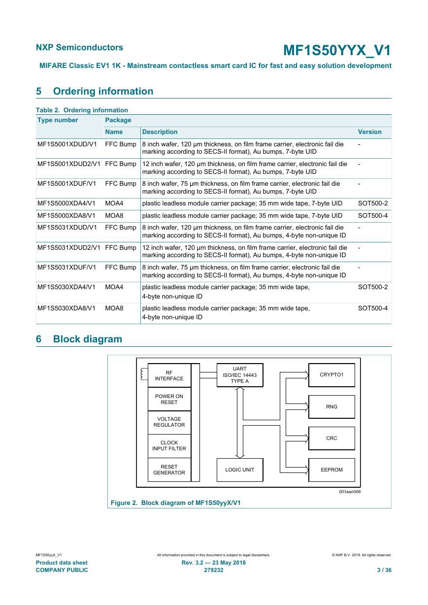
6 Block diagram
Version
-
-
-
SOT500-2
SOT500-4
-
-
-
SOT500-2
SOT500-4
RF
INTERFACE
POWER ON
RESET
VOLTAGE
REGULATOR
CLOCK
INPUT FILTER
RESET
GENERATOR
UART
ISO/IEC 14443
TYPE A
CRYPTO1
RNG
CRC
LOGIC UNIT
EEPROM
001aan006
Figure 2. Block diagram of MF1S50yyX/V1
MF1S50yyX_V1
Product data sheet
COMPANY PUBLIC
All information provided in this document is subject to legal disclaimers.
© NXP B.V. 2018. All rights reserved.
Rev. 3.2 — 23 May 2018
279232
3 / 36
�
NXP Semiconductors
MF1S50YYX_V1
MIFARE Classic EV1 1K - Mainstream contactless smart card IC for fast and easy solution development
7 Pinning information
7.1 Pinning
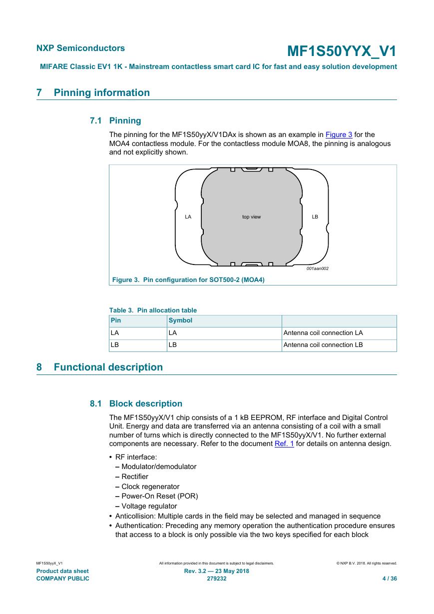
The pinning for the MF1S50yyX/V1DAx is shown as an example in Figure 3 for the
MOA4 contactless module. For the contactless module MOA8, the pinning is analogous
and not explicitly shown.
LA
top view
LB
Figure 3. Pin configuration for SOT500-2 (MOA4)
001aan002
Table 3. Pin allocation table
Symbol
Pin
LA
LA
LB
LB
Antenna coil connection LA
Antenna coil connection LB
8 Functional description
8.1 Block description
The MF1S50yyX/V1 chip consists of a 1 kB EEPROM, RF interface and Digital Control
Unit. Energy and data are transferred via an antenna consisting of a coil with a small
number of turns which is directly connected to the MF1S50yyX/V1. No further external
components are necessary. Refer to the document Ref. 1 for details on antenna design.
• RF interface:
– Modulator/demodulator
– Rectifier
– Clock regenerator
– Power-On Reset (POR)
– Voltage regulator
• Anticollision: Multiple cards in the field may be selected and managed in sequence
• Authentication: Preceding any memory operation the authentication procedure ensures
that access to a block is only possible via the two keys specified for each block
MF1S50yyX_V1
Product data sheet
COMPANY PUBLIC
All information provided in this document is subject to legal disclaimers.
© NXP B.V. 2018. All rights reserved.
Rev. 3.2 — 23 May 2018
279232
4 / 36
�
NXP Semiconductors
MF1S50YYX_V1
MIFARE Classic EV1 1K - Mainstream contactless smart card IC for fast and easy solution development
• Control and Arithmetic Logic Unit: Values are stored in a special redundant format and
can be incremented and decremented
• EEPROM interface
• Crypto unit: The CRYPTO1 stream cipher of the MF1S50yyX/V1 is used for
authentication and encryption of data exchange.
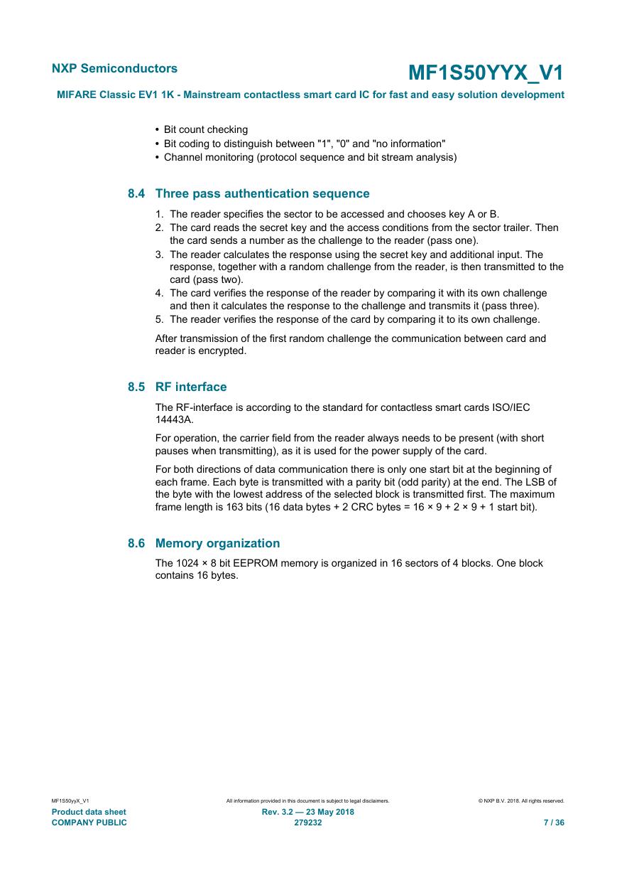
• EEPROM: 1 kB is organized in 16 sectors of 4 blocks. One block contains 16 bytes.
The last block of each sector is called "trailer", which contains two secret keys and
programmable access conditions for each block in this sector.
8.2 Communication principle
The commands are initiated by the reader and controlled by the Digital Control Unit of
the MF1S50yyX/V1. The command response is depending on the state of the IC and for
memory operations also on the access conditions valid for the corresponding sector.
8.2.1 Request standard / all
After Power-On Reset (POR) the card answers to a request REQA or wakeup WUPA
command with the answer to request code (see Section 9.4, ATQA according to ISO/IEC
14443A).
8.2.2 Anticollision loop
In the anticollision loop the identifier of a card is read. If there are several cards in the
operating field of the reader, they can be distinguished by their identifier and one can
be selected (select card) for further transactions. The unselected cards return to the idle
state and wait for a new request command. If the 7-byte UID is used for anticollision and
selection, two cascade levels need to be processes as defined in ISO/IEC 14443-3.
Remark: For the 4-byte non-unique ID product versions, the identifier retrieved from the
card is not defined to be unique. For further information regarding handling of non-unique
identifiers see Ref. 6.
8.2.3 Select card
With the select card command the reader selects one individual card for authentication
and memory related operations. The card returns the Select AcKnowledge (SAK) code
which determines the type of the selected card, see Section 9.4. For further details refer
to the document Ref. 2.
8.2.4 Three pass authentication
After selection of a card the reader specifies the memory location of the following
memory access and uses the corresponding key for the three pass authentication
procedure. After a successful authentication all commands and responses are encrypted.
Remark: The HLTA command needs to be sent encrypted to the PICC after a successful
authentication in order to be accepted.
MF1S50yyX_V1
Product data sheet
COMPANY PUBLIC
All information provided in this document is subject to legal disclaimers.
© NXP B.V. 2018. All rights reserved.
Rev. 3.2 — 23 May 2018
279232
5 / 36
�
NXP Semiconductors
MF1S50YYX_V1
MIFARE Classic EV1 1K - Mainstream contactless smart card IC for fast and easy solution development
POR
Transaction Sequence
Typical Transaction Time
Request Standard
Request All
Anticollision Loop
Get Identifier
Select Card
3 Pass Authenticationon
specific sector
Read
Block
Write
Block
Decre-
ment
Incre-
ment
Re-
store
Halt
Transfer
Identification and Selection
Procedure
~2.5 ms without collision
for 7-byte UID
+ ~1 ms
+ ~1 ms
for each collision
Authentication Procedure
~2 ms
Memory Operations
~2.5 ms
read block
~5.5 ms write block
~2.5 ms
~4.5 ms
de-/increment
transfer
001aan921
1.
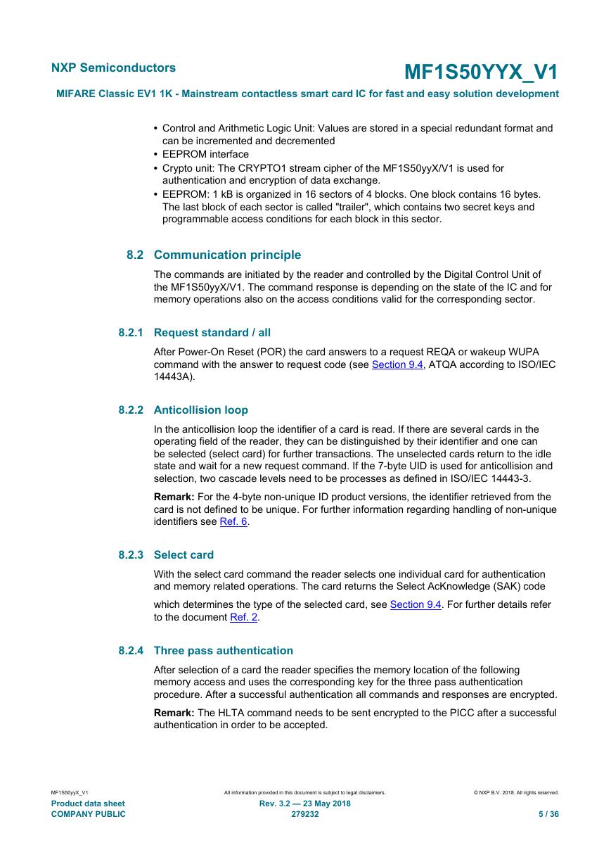
the command flow diagram does not include the Personalize UID Usage and the
SET_MOD_TYPE command, for details on those commands please see Section 10.1.1 and
Section 11
Figure 4. MIFARE Classic command flow diagram
8.2.5 Memory operations
After authentication any of the following operations may be performed:
• Read block
• Write block
• Decrement: Decrements the contents of a block and stores the result in the internal
Transfer Buffer
• Increment: Increments the contents of a block and stores the result in the internal
Transfer Buffer
• Restore: Moves the contents of a block into the internal Transfer Buffer
• Transfer: Writes the contents of the internal Transfer Buffer to a value block
8.3 Data integrity
Following mechanisms are implemented in the contactless communication link between
reader and card to ensure very reliable data transmission:
• 16 bits CRC per block
• Parity bits for each byte
All information provided in this document is subject to legal disclaimers.
© NXP B.V. 2018. All rights reserved.
Rev. 3.2 — 23 May 2018
279232
6 / 36
MF1S50yyX_V1
Product data sheet
COMPANY PUBLIC
�
NXP Semiconductors
MF1S50YYX_V1
MIFARE Classic EV1 1K - Mainstream contactless smart card IC for fast and easy solution development
• Bit count checking
• Bit coding to distinguish between "1", "0" and "no information"
• Channel monitoring (protocol sequence and bit stream analysis)
8.4 Three pass authentication sequence
1. The reader specifies the sector to be accessed and chooses key A or B.
2. The card reads the secret key and the access conditions from the sector trailer. Then
the card sends a number as the challenge to the reader (pass one).
3. The reader calculates the response using the secret key and additional input. The
response, together with a random challenge from the reader, is then transmitted to the
card (pass two).
4. The card verifies the response of the reader by comparing it with its own challenge
and then it calculates the response to the challenge and transmits it (pass three).
5. The reader verifies the response of the card by comparing it to its own challenge.
After transmission of the first random challenge the communication between card and
reader is encrypted.
8.5 RF interface
The RF-interface is according to the standard for contactless smart cards ISO/IEC
14443A.
For operation, the carrier field from the reader always needs to be present (with short
pauses when transmitting), as it is used for the power supply of the card.
For both directions of data communication there is only one start bit at the beginning of
each frame. Each byte is transmitted with a parity bit (odd parity) at the end. The LSB of
the byte with the lowest address of the selected block is transmitted first. The maximum
frame length is 163 bits (16 data bytes + 2 CRC bytes = 16 × 9 + 2 × 9 + 1 start bit).
8.6 Memory organization
The 1024 × 8 bit EEPROM memory is organized in 16 sectors of 4 blocks. One block
contains 16 bytes.
MF1S50yyX_V1
Product data sheet
COMPANY PUBLIC
All information provided in this document is subject to legal disclaimers.
© NXP B.V. 2018. All rights reserved.
Rev. 3.2 — 23 May 2018
279232
7 / 36
�
NXP Semiconductors
MF1S50YYX_V1
MIFARE Classic EV1 1K - Mainstream contactless smart card IC for fast and easy solution development
Sector
Block
0
1
2
3
4
5
6
7
8
9
10
11
12
13
14
15
Description
Byte Number within a Block
15
14
:
:
:
1
0
3
2
1
0
3
2
1
0
:
:
:
3
2
1
0
3
2
1
0
Key A
Access Bits
Key B
Sector Trailer 15
Data
Data
Data
Key A
Access Bits
Key B
Sector Trailer 14
Data
Data
Data
Key A
Access Bits
Key B
Sector Trailer 1
Data
Data
Data
Key A
Access Bits
Key B
Sector Trailer 0
Manufacturer Data
Data
Data
Manufacturer Block
001aan011
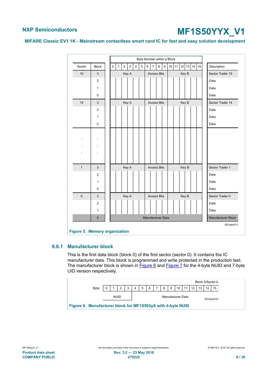
Figure 5. Memory organization
8.6.1 Manufacturer block
This is the first data block (block 0) of the first sector (sector 0). It contains the IC
manufacturer data. This block is programmed and write protected in the production test.
The manufacturer block is shown in Figure 6 and Figure 7 for the 4-byte NUID and 7-byte
UID version respectively.
Byte
0
1
2
3
4
5
6
7
8
9
10
11
12
Block 0/Sector 0
15
13
14
NUID
Manufacturer Data
001aan010
Figure 6. Manufacturer block for MF1S503yX with 4-byte NUID
MF1S50yyX_V1
Product data sheet
COMPANY PUBLIC
All information provided in this document is subject to legal disclaimers.
© NXP B.V. 2018. All rights reserved.
Rev. 3.2 — 23 May 2018
279232
8 / 36
�




 V2版本原理图(Capacitive-Fingerprint-Reader-Schematic_V2).pdf
 摄像头工作原理.doc
 VL53L0X简要说明(En.FLVL53L00216).pdf
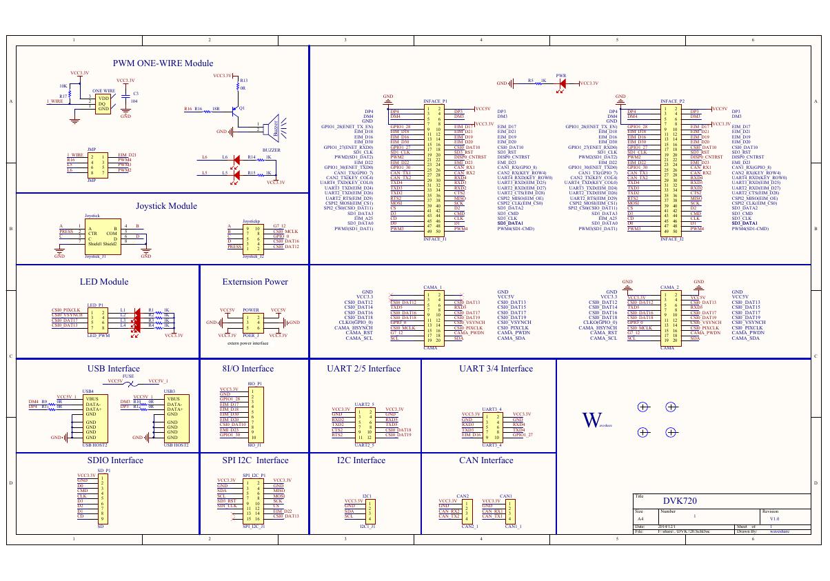 原理图(DVK720-Schematic).pdf
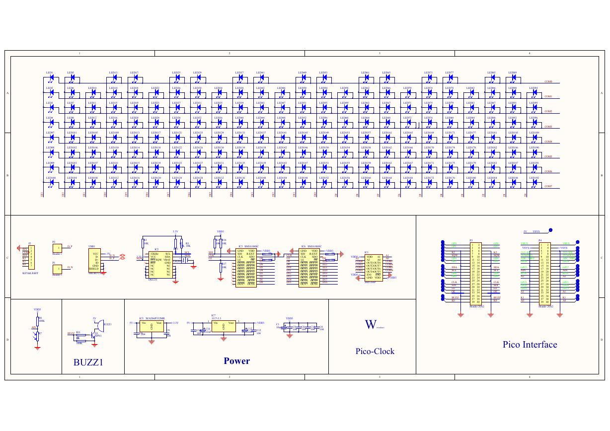 原理图(Pico-Clock-Green-Schdoc).pdf
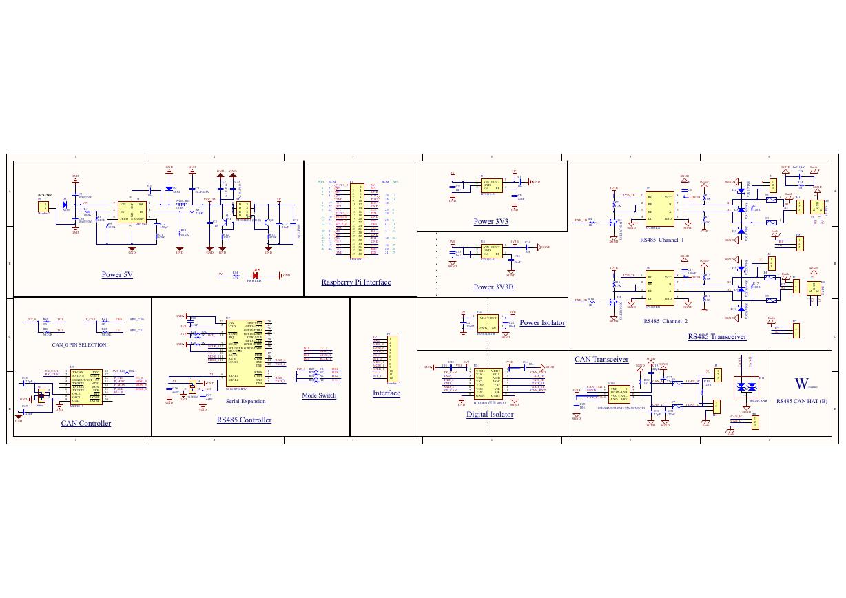 原理图(RS485-CAN-HAT-B-schematic).pdf
 File:SIM7500_SIM7600_SIM7800 Series_SSL_Application Note_V2.00.pdf
 ADS1263(Ads1262).pdf
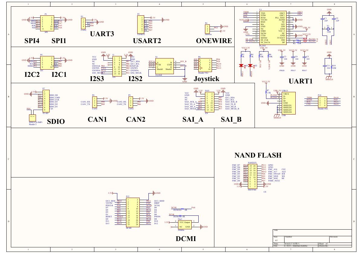 原理图(Open429Z-D-Schematic).pdf
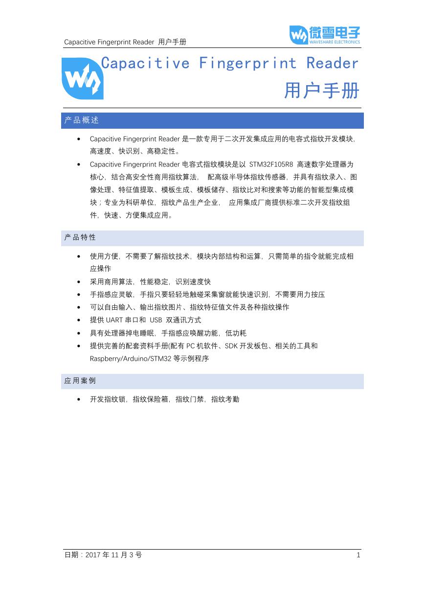 用户手册(Capacitive_Fingerprint_Reader_User_Manual_CN).pdf
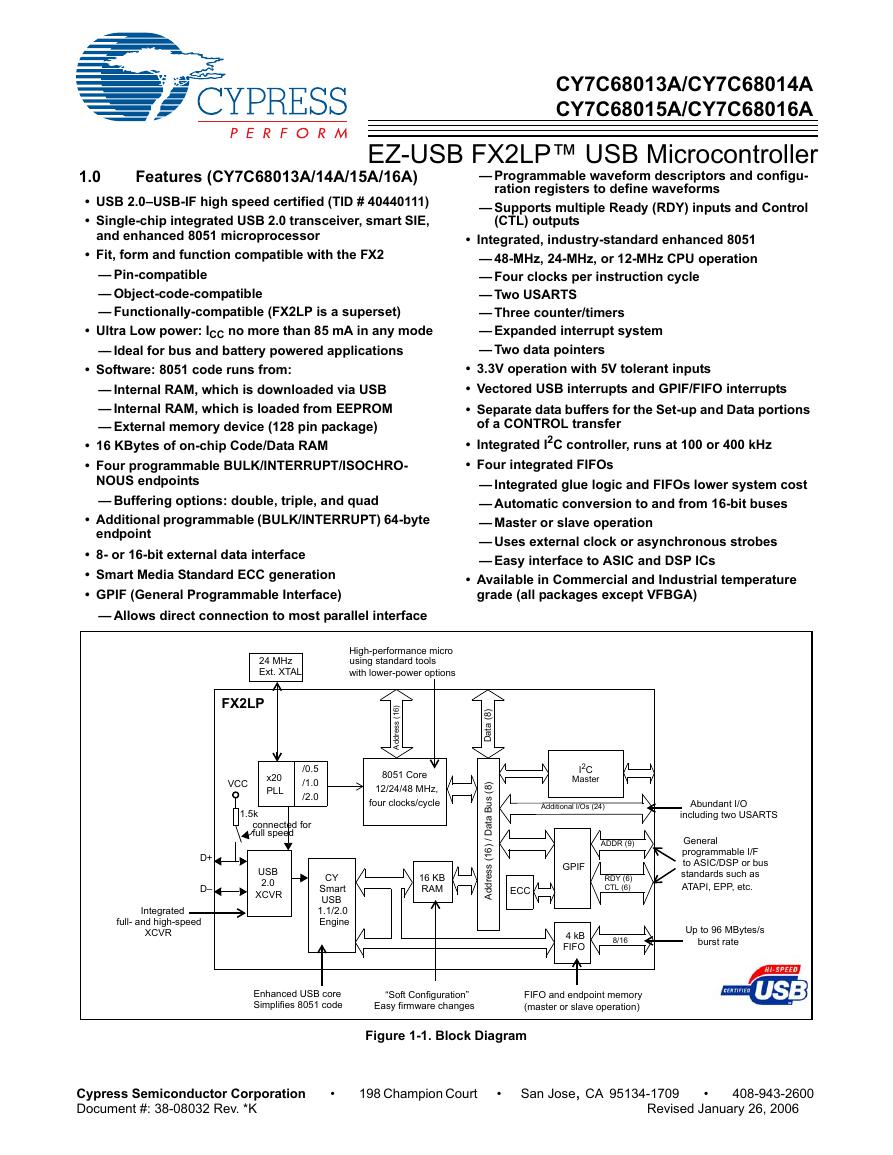 CY7C68013A(英文版)(CY7C68013A).pdf
 TechnicalReference_Dem.pdf