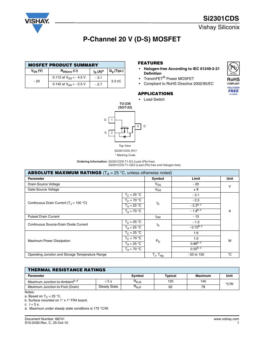
P-Channel 20 V (D-S) MOSFET
Si2301CDS
Vishay Siliconix
MOSFET PRODUCT SUMMARY
ID (A)a
- 3.1
RDS(on) ()
VDS (V)
- 20
0.112 at VGS = - 4.5 V
0.142 at VGS = - 2.5 V
- 2.7
Qg (Typ.)
3.3 nC
FEATURES
• Halogen-free According to IEC 61249-2-21
Definition
TrenchFET® Power MOSFET
Compliant to RoHS Directive 2002/95/EC
APPLICATIONS
Load Switch
TO-236
(SOT-23)
G
1
S
2
3
D
Top View
Si2301CDS (N1)*
* Marking Code
Ordering Information: Si2301CDS-T1-E3 (Lead (Pb)-free)
Si2301CDS-T1-GE3 (Lead (Pb)-free and Halogen-free)
ABSOLUTE MAXIMUM RATINGS (TA = 25 °C, unless otherwise noted)
Parameter
Drain-Source Voltage
Gate-Source Voltage
Symbol
VDS
VGS
Continuous Drain Current (TJ = 150 °C)
Pulsed Drain Current
Continuous Source-Drain Diode Current
Maximum Power Dissipation
TC = 25 °C
TC = 70 °C
TA = 25 °C
TA = 70 °C
TC = 25 °C
TA = 25 °C
TC = 25 °C
TC = 70 °C
TA = 25 °C
TA = 70 °C
ID
IDM
IS
PD
Limit
- 20
± 8
- 3.1
- 2.5
- 2.3b, c
- 1.8b, c
- 10
- 1.3
- 0.72b, c
1.6
1.0
0.86b, c
0.55b, c
Operating Junction and Storage Temperature Range
TJ, Tstg
- 55 to 150
Unit
V
A
W
°C
THERMAL RESISTANCE RATINGS
Parameter
Maximum Junction-to-Ambientb, d
Maximum Junction-to-Foot (Drain)
5 s
Steady State
Notes:
a. Based on TC = 25 °C.
b. Surface mounted on 1" x 1" FR4 board.
c. t = 5 s.
d. Maximum under steady state conditions is 175 °C/W.
Document Number: 68741
S10-2430-Rev. C, 25-Oct-10
Symbol
RthJA
RthJF
Typical
120
62
Maximum
145
78
Unit
°C/W
www.vishay.com
1
�
Si2301CDS
Vishay Siliconix
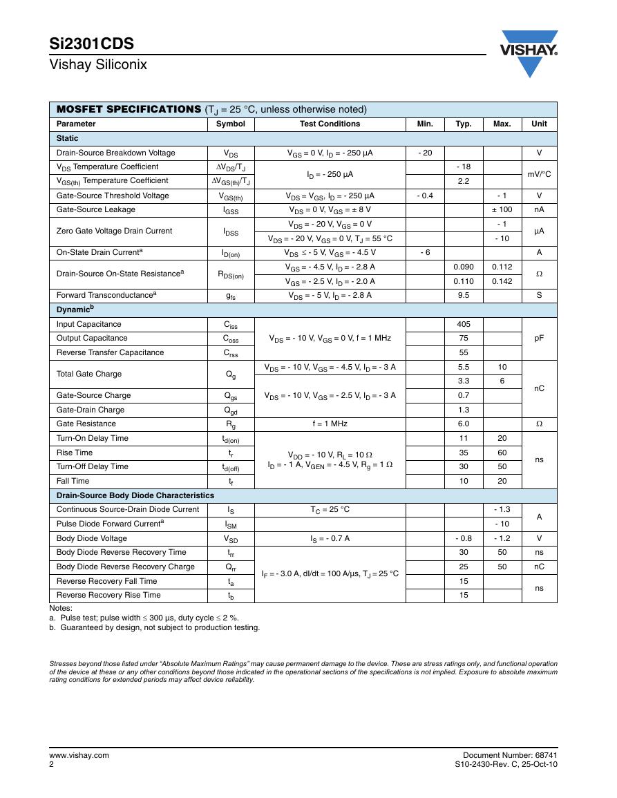
MOSFET SPECIFICATIONS (TJ = 25 °C, unless otherwise noted)
Parameter
Test Conditions
Static
Symbol
Min.
Typ.
Max.
Unit
Drain-Source Breakdown Voltage
VDS Temperature Coefficient
VGS(th) Temperature Coefficient
Gate-Source Threshold Voltage
Gate-Source Leakage
Zero Gate Voltage Drain Current
On-State Drain Currenta
Drain-Source On-State Resistancea
Forward Transconductancea
Dynamicb
Input Capacitance
Output Capacitance
Reverse Transfer Capacitance
Total Gate Charge
Gate-Source Charge
Gate-Drain Charge
Gate Resistance
Turn-On Delay Time
Rise Time
Turn-Off Delay Time
Fall Time
Drain-Source Body Diode Characteristics
Continuous Source-Drain Diode Current
Pulse Diode Forward Currenta
Body Diode Voltage
Body Diode Reverse Recovery Time
Body Diode Reverse Recovery Charge
Reverse Recovery Fall Time
Reverse Recovery Rise Time
VDS
VDS/TJ
VGS(th)/TJ
VGS(th)
IGSS
IDSS
ID(on)
RDS(on)
gfs
Ciss
Coss
Crss
Qg
Qgs
Qgd
Rg
td(on)
tr
td(off)
tf
IS
ISM
VSD
trr
Qrr
ta
tb
VGS = 0 V, ID = - 250 µA
- 20
ID = - 250 µA
VDS = VGS, ID = - 250 µA
VDS = 0 V, VGS = ± 8 V
VDS = - 20 V, VGS = 0 V
VDS = - 20 V, VGS = 0 V, TJ = 55 °C
VDS - 5 V, VGS = - 4.5 V
VGS = - 4.5 V, ID = - 2.8 A
VGS = - 2.5 V, ID = - 2.0 A
VDS = - 5 V, ID = - 2.8 A
- 0.4
- 6
VDS = - 10 V, VGS = 0 V, f = 1 MHz
VDS = - 10 V, VGS = - 4.5 V, ID = - 3 A
VDS = - 10 V, VGS = - 2.5 V, ID = - 3 A
f = 1 MHz
VDD = - 10 V, RL = 10
ID = - 1 A, VGEN = - 4.5 V, Rg = 1
TC = 25 °C
IS = - 0.7 A
IF = - 3.0 A, dI/dt = 100 A/µs, TJ = 25 °C
V
mV/°C
V
nA
µA
A
S
pF
nC
ns
A
V
ns
nC
ns
- 1
± 100
- 1
- 10
0.112
0.142
10
6
20
60
50
20
- 1.3
- 10
- 1.2
50
50
- 18
2.2
0.090
0.110
9.5
405
75
55
5.5
3.3
0.7
1.3
6.0
11
35
30
10
- 0.8
30
25
15
15
Notes:
a. Pulse test; pulse width 300 µs, duty cycle 2 %.
b. Guaranteed by design, not subject to production testing.
Stresses beyond those listed under “Absolute Maximum Ratings” may cause permanent damage to the device. These are stress ratings only, and functional operation
of the device at these or any other conditions beyond those indicated in the operational sections of the specifications is not implied. Exposure to absolute maximum
rating conditions for extended periods may affect device reliability.
www.vishay.com
2
Document Number: 68741
S10-2430-Rev. C, 25-Oct-10
�
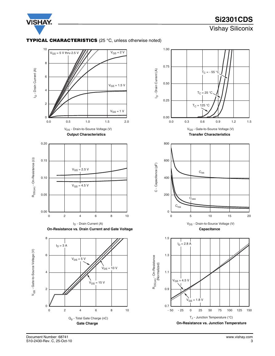
TYPICAL CHARACTERISTICS (25 °C, unless otherwise noted)
VGS = 5 V thru 2.5 V
VGS = 2 V
)
A
(
t
1.00
0.75
0.50
n
e
r
r
u
C
n
a
r
D
i
-
D
I
0.25
0.00
VGS = 1.5 V
VGS = 1 V
Si2301CDS
Vishay Siliconix
TC = - 55 °C
TC = 25 °C
TC = 125 °C
10
8
6
4
2
)
A
(
t
n
e
r
r
u
C
n
a
r
D
i
-
D
I
0
0.0
0.20
0.15
0.10
0.05
0.00
0
)
Ω
(
i
e
c
n
a
t
s
s
e
R
-
n
O
-
)
n
o
(
S
D
R
)
V
(
e
g
a
t
l
o
V
e
c
r
u
o
S
-
o
t
-
e
t
a
G
-
S
G
V
0.5
1.0
1.5
2.0
0.0
0.3
0.6
0.9
1.2
1.5
VDS - Drain-to-Source Voltage (V)
Output Characteristics
VGS - Gate-to-Source Voltage (V)
Transfer Characteristics
)
F
p
(
e
c
n
a
t
i
c
a
p
a
C
-
C
VGS = 2.5 V
VGS = 4.5 V
2
4
6
8
10
ID - Drain Current (A)
On-Resistance vs. Drain Current and Gate Voltage
ID = 3 A
VDS = 5 V
e
c
n
a
VDS = 10 V
VDS = 15 V
)
d
e
z
i
l
a
m
r
o
N
(
i
t
s
s
e
R
-
n
O
-
)
n
o
(
S
D
R
8
6
4
2
0
800
600
400
200
Crss
0
0
Ciss
Coss
5
10
15
20
VDS - Drain-to-Source Voltage (V)
Capacitance
1.5
1.3
1.1
0.9
0.7
ID = 2.8 A
VGS = 4.5 V
VGS = 1.8 V
0
2
4
6
8
10
- 50
- 25
0
25
50
75
100
125
150
Qg - Total Gate Charge (nC)
Gate Charge
TJ - Junction Temperature (°C)
On-Resistance vs. Junction Temperature
Document Number: 68741
S10-2430-Rev. C, 25-Oct-10
www.vishay.com
3
�
Si2301CDS
Vishay Siliconix
TYPICAL CHARACTERISTICS (25 °C, unless otherwise noted)
)
A
(
t
n
e
r
r
u
C
e
c
r
u
o
S
-
S
I
10
1
0.1
TJ = 150 °C
TJ = 25 °C
TJ = - 50 °C
0.0
0.2
0.4
0.6
0.8
1.0
1.2
1.4
VSD - Source-to-Drain Voltage (V)
Source-Drain Diode Forward Voltage
)
V
(
e
c
n
a
i
r
a
V
)
h
t
(
S
G
V
0.4
0.3
0.2
0.1
0.0
- 0.1
- 0.2
ID = 250 µA
ID = 1 mA
- 50
- 25
0
25
50
75
100
125
150
TJ - Temperature (°C)
Threshold Voltage
10
Limited by RDS(on)*
)
Ω
(
e
c
n
a
i
t
s
s
e
R
-
n
O
-
)
n
o
(
S
D
R
0.60
0.45
0.30
0.15
0.00
0
10
8
6
4
2
)
W
(
r
e
w
o
P
ID = 2.8 A
TJ = 125 °C
TJ = 25 °C
1
2
3
4
5
VGS - Gate-to-Source Voltage (V)
On-Resistance vs. Gate-to-Source Voltage
TA = 25 °C
0
0.01
0.1
1
10
100
1000
Time (s)
Single Pulse Power
100 µs
1 ms
10 ms
100 ms
1 s
10 s
100 s, DC
)
A
(
t
n
e
r
r
u
C
n
a
r
D
i
-
D
I
1
0.1
0.01
0.1
TA = 25 °C
Single Pulse
BVDSS Limited
1
10
100
VDS - Drain-to-Source Voltage (V)
* VGS > minimum VGS at which RDS(on) is specified
Safe Operating Area
www.vishay.com
4
Document Number: 68741
S10-2430-Rev. C, 25-Oct-10
�
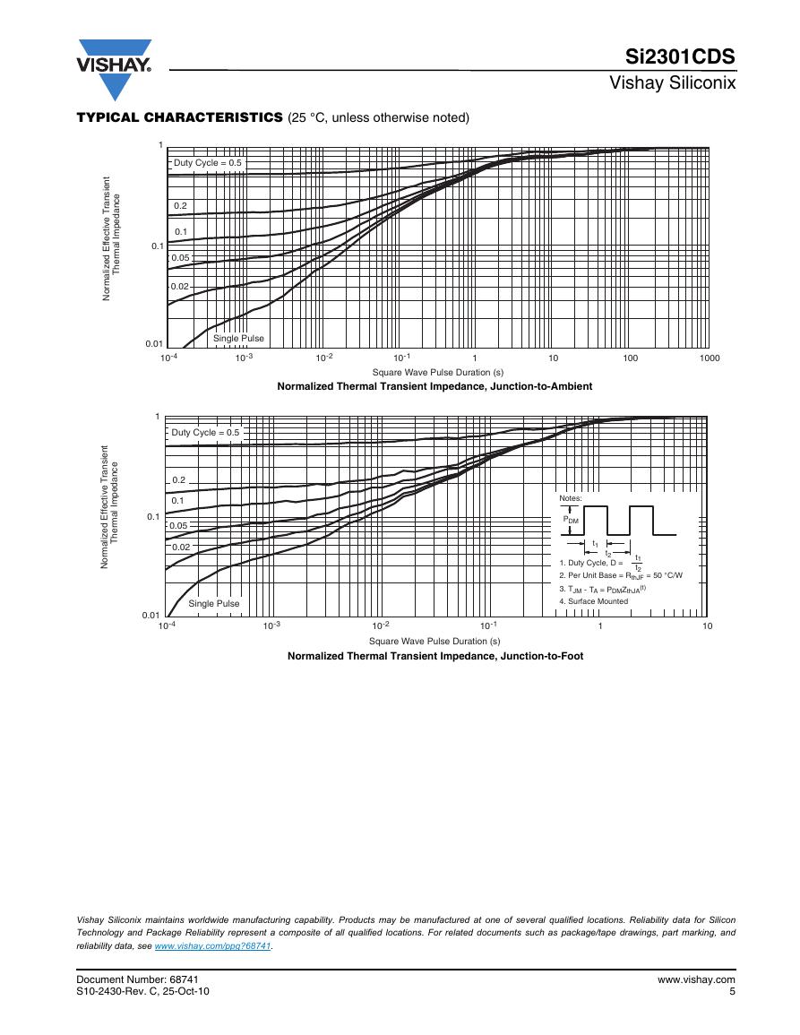
TYPICAL CHARACTERISTICS (25 °C, unless otherwise noted)
Si2301CDS
Vishay Siliconix
e
c
n
a
d
e
p
m
I
l
a
m
r
e
h
T
t
i
n
e
s
n
a
r
T
e
v
i
t
c
e
f
f
E
d
e
z
i
l
a
m
r
o
N
1
0.1
Duty Cycle = 0.5
0.2
0.1
0.05
0.02
0.01
10-4
Single Pulse
10-3
10-2
10-1
1
10
100
1000
Normalized Thermal Transient Impedance, Junction-to-Ambient
Square Wave Pulse Duration (s)
e
c
n
a
d
e
p
m
I
l
a
m
r
e
h
T
i
t
n
e
s
n
a
r
T
e
v
i
t
c
e
f
f
E
d
e
z
i
l
a
m
r
o
N
1
0.1
Duty Cycle = 0.5
0.2
0.1
0.05
0.02
Single Pulse
0.01
10-4
10-3
Notes:
PDM
t1
t2
t1
t2
1. Duty Cycle, D =
2. Per Unit Base = RthJF = 50 °C/W
3. TJM - TA = PDMZthJA
4. Surface Mounted
(t)
10-1
10-2
Square Wave Pulse Duration (s)
1
01
Normalized Thermal Transient Impedance, Junction-to-Foot
Vishay Siliconix maintains worldwide manufacturing capability. Products may be manufactured at one of several qualified locations. Reliability data for Silicon
Technology and Package Reliability represent a composite of all qualified locations. For related documents such as package/tape drawings, part marking, and
reliability data, see www.vishay.com/ppg?68741.
Document Number: 68741
S10-2430-Rev. C, 25-Oct-10
www.vishay.com
5
�
Package Information
Vishay Siliconix
SOT-23 (TO-236): 3-LEAD
b
3
1
2
E1
E
S
e
e1
D
A
A2
A1
Dim
A
A1
A2
b
c
D
E
E1
e
e1
L
L1
S
q
0.10 mm
0.004"
C
Seating Plane
C
C
q
0.25 mm
Gauge Plane
Seating Plane
L
L1
MILLIMETERS
INCHES
Min
0.89
0.01
0.88
0.35
0.085
2.80
2.10
1.20
0.40
3°
0.95 BSC
1.90 BSC
0.64 Ref
0.50 Ref
Max
1.12
0.10
1.02
0.50
0.18
3.04
2.64
1.40
0.60
8°
Min
0.035
0.0004
0.0346
0.014
0.003
0.110
0.083
0.047
0.016
3°
0.0374 Ref
0.0748 Ref
0.025 Ref
0.020 Ref
Max
0.044
0.004
0.040
0.020
0.007
0.120
0.104
0.055
0.024
8°
ECN: S-03946-Rev. K, 09-Jul-01
DWG: 5479
Document Number: 71196
09-Jul-01
www.vishay.com
1
�
AN807
Vishay Siliconix
Mounting LITTLE FOOTR SOT-23 Power MOSFETs
Wharton McDaniel
Surface-mounted LITTLE FOOT power MOSFETs use integrated
circuit and small-signal packages which have been been modified
to provide the heat transfer capabilities required by power devices.
Leadframe materials and design, molding compounds, and die
attach materials have been changed, while the footprint of the
packages remains the same.
See Application Note 826, Recommended Minimum Pad
Patterns With Outline Drawing Access for Vishay Siliconix
MOSFETs, (http://www.vishay.com/doc?72286), for the basis
of the pad design for a LITTLE FOOT SOT-23 power MOSFET
footprint . In converting this footprint to the pad set for a power
device, designers must make two connections: an electrical
connection and a thermal connection, to draw heat away from the
package.
ambient air. This pattern uses all the available area underneath the
body for this purpose.
0.114
2.9
0.081
2.05
0.150
3.8
0.059
1.5
0.0394
1.0
0.037
0.95
FIGURE 1. Footprint With Copper Spreading
The electrical connections for the SOT-23 are very simple. Pin 1 is
the gate, pin 2 is the source, and pin 3 is the drain. As in the other
LITTLE FOOT packages, the drain pin serves the additional
function of providing the thermal connection from the package to
the PC board. The total cross section of a copper trace connected
to the drain may be adequate to carry the current required for the
application, but it may be inadequate thermally. Also, heat spreads
in a circular fashion from the heat source. In this case the drain pin
is the heat source when looking at heat spread on the PC board.
Since surface-mounted packages are small, and reflow soldering
is the most common way in which these are affixed to the PC
board, “thermal” connections from the planar copper to the pads
have not been used. Even if additional planar copper area is used,
there should be no problems in the soldering process. The actual
solder connections are defined by the solder mask openings. By
combining the basic footprint with the copper plane on the drain
pins, the solder mask generation occurs automatically.
Figure 1 shows the footprint with copper spreading for the SOT-23
package. This pattern shows the starting point for utilizing the
board area available for the heat spreading copper. To create this
pattern, a plane of copper overlies the drain pin and provides
planar copper to draw heat from the drain lead and start the
process of spreading the heat so it can be dissipated into the
A final item to keep in mind is the width of the power traces. The
absolute minimum power trace width must be determined by the
amount of current it has to carry. For thermal reasons, this
minimum width should be at least 0.020 inches. The use of wide
traces connected to the drain plane provides a low-impedance
path for heat to move away from the device.
Document Number: 70739
26-Nov-03
www.vishay.com
1
�
Application Note 826
Vishay Siliconix
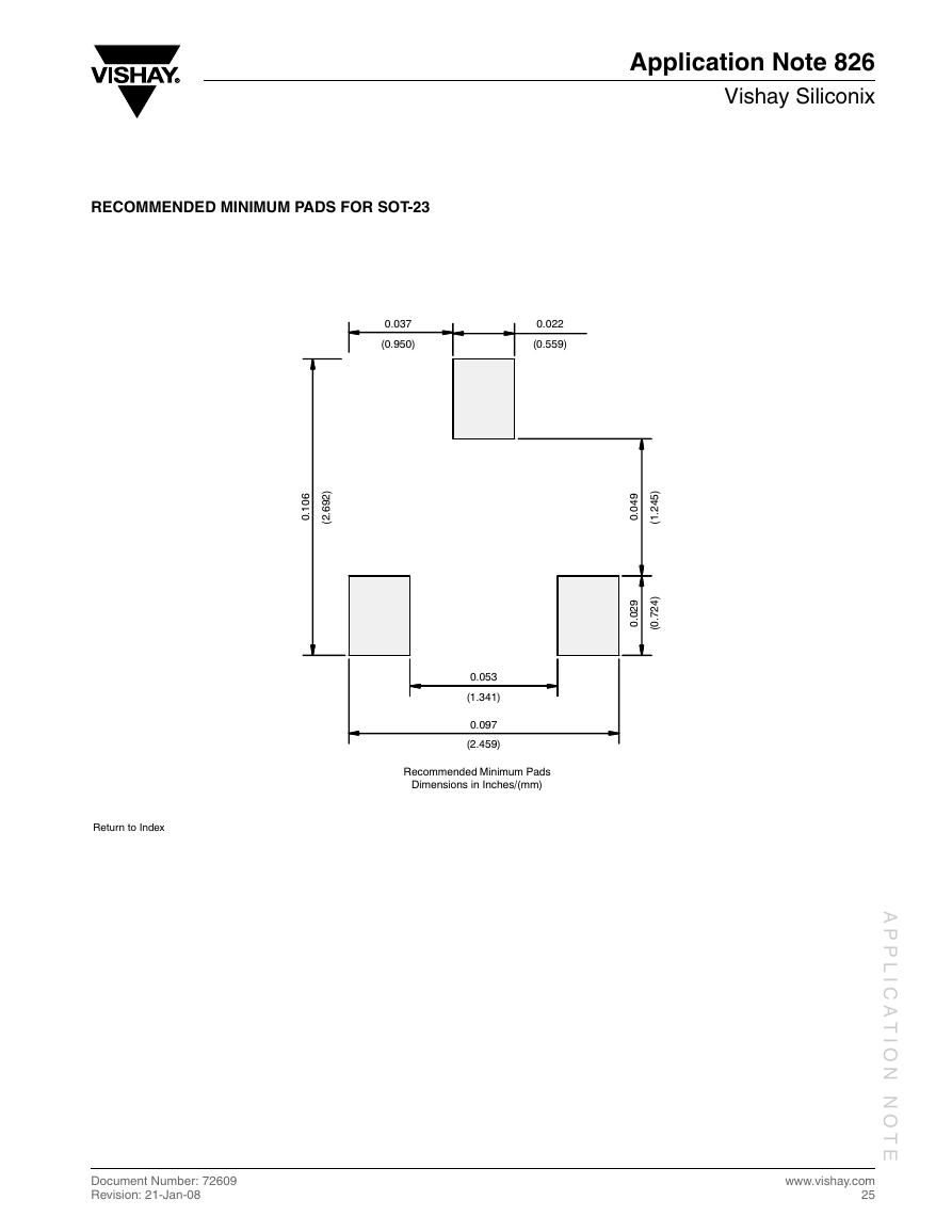
RECOMMENDED MINIMUM PADS FOR SOT-23
0.037
(0.950)
0.022
(0.559)
6
0
1
.
0
)
2
9
6
.
2
(
9
4
0
.
0
)
5
4
2
.
1
(
9
2
0
.
0
)
4
2
7
.
0
(
0.053
(1.341)
0.097
(2.459)
Recommended Minimum Pads
Dimensions in Inches/(mm)
Return to Index
Return to Index
A
P
P
L
I
C
A
T
I
O
N
N
O
T
E
Document Number: 72609
Revision: 21-Jan-08
www.vishay.com
25
�





 V2版本原理图(Capacitive-Fingerprint-Reader-Schematic_V2).pdf
 摄像头工作原理.doc
 VL53L0X简要说明(En.FLVL53L00216).pdf
 原理图(DVK720-Schematic).pdf
 原理图(Pico-Clock-Green-Schdoc).pdf
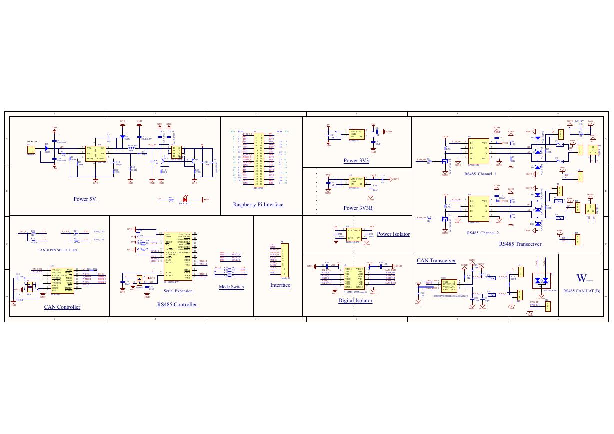 原理图(RS485-CAN-HAT-B-schematic).pdf
 File:SIM7500_SIM7600_SIM7800 Series_SSL_Application Note_V2.00.pdf
 ADS1263(Ads1262).pdf
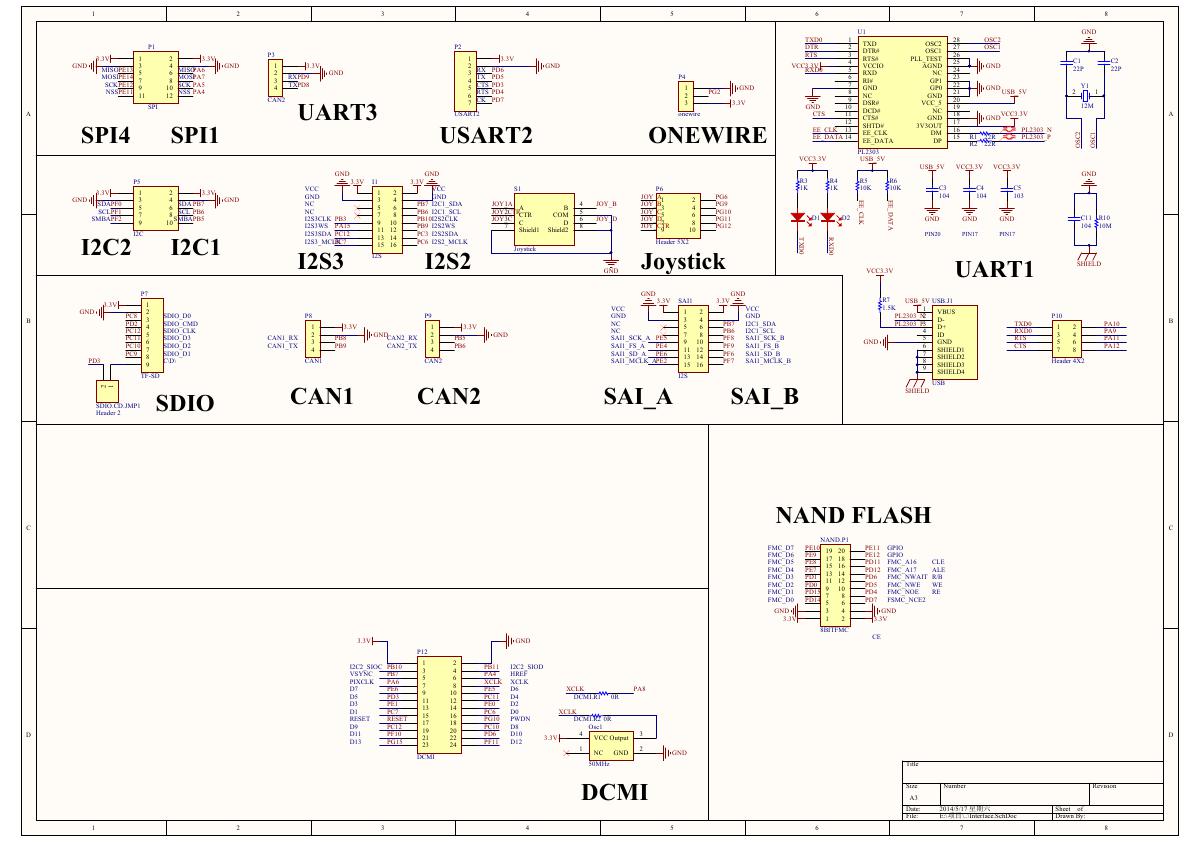 原理图(Open429Z-D-Schematic).pdf
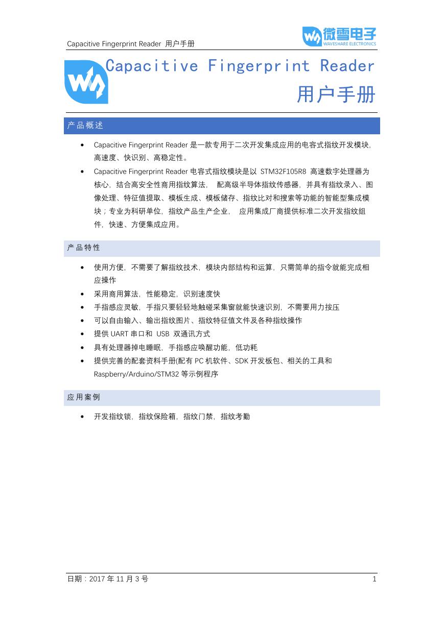 用户手册(Capacitive_Fingerprint_Reader_User_Manual_CN).pdf
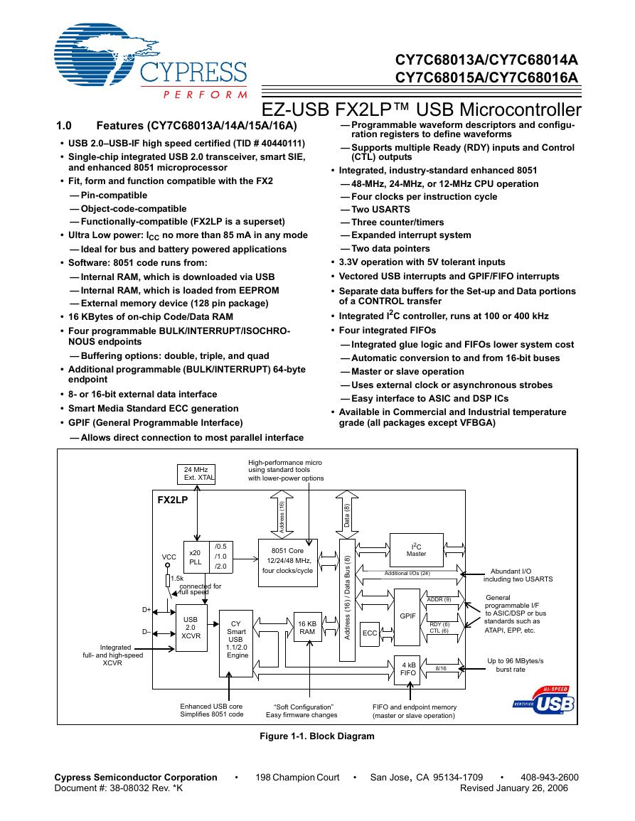 CY7C68013A(英文版)(CY7C68013A).pdf
 TechnicalReference_Dem.pdf