AR0130CS
1/3‐inch CMOS Digital
Image Sensor
Description
ON Semiconductor AR0130 is a 1/3−inch CMOS digital image
sensor with an active−pixel array of 1280H x 960V. It captures images
with a rolling−shutter readout. It includes sophisticated camera
functions such as auto exposure control, windowing, and both video
and single frame modes. It is programmable through a simple
two−wire serial interface. The AR0130 produces extraordinarily clear,
sharp digital pictures, and its ability to capture both continuous video
and single frames makes it the perfect choice for a wide range of
applications, including gaming systems, surveillance, and HD video.
Table 1. KEY PERFORMANCE PARAMETERS
Parameter
Typical Value
Optical Format
Active Pixels
Pixel Size
Color Filter Array
Shutter Type
Input Clock Range
Output Clock Maximum
Output
Parallel
Max. Frame Rates
1.2 Mp (Full FOV)
720p HD (Reduced FOV)
VGA (Full FOV)
VGA (Reduced FOV)
800 x 800 (Reduced FOV)
Responsivity at 550 nm
Monochrome
RGB Green
SNRMAX
Dynamic Range
Supply Voltage
I/O
Digital
Analog
Power Consumption
Operating Temperature
Package Options
1/3-inch (6 mm)
1280 (H) × 960 (V) = 1.2 Mp
3.75 mm
Monochrome, RGB Bayer
Electronic Rolling Shutter
6 – 50 MHz
74.25 MHz
12-bit
45 fps
60 fps
45 fps
60 fps
60 fps
6.5 V/lux−sec
5.6 V/lux−sec
44 dB
82 dB
1.8 or 2.8 V
1.8 V
2.8 V
270 mW (1280 x 720 60 fps)
–30°C to + 70°C (Ambient)
–30°C to + 80°C (Junction)
PLCC
10 × 10 mm 48-pin iLCC
Bare Die
www.onsemi.com
PLCC48 11.43 y 11.43
CASE 776AL
ILCC48 10 y 10
CASE 847AC
ORDERING INFORMATION
See detailed ordering and shipping information on page 2 of
this data sheet.
VGA Mode and HD Mode
Features
• Superior Low-light Performance Both in
• Excellent Near IR Performance
• HD Video (720p60)
• On-chip AE and Statistics Engine
• Auto Black Level Calibration
• Context Switching
• Progressive Scan
• Supports 2:1 Scaling
• Internal Master Clock Generated by
On−chip Phase Locked Loop (PLL)
Oscillator
• Parallel Output
Applications
• Gaming Systems
• Video Surveillance
• 720p60 Video Applications
© Semiconductor Components Industries, LLC, 2016
January, 2019 − Rev. 15
1
Publication Order Number:
AR0130CS/D
�
AR0130CS
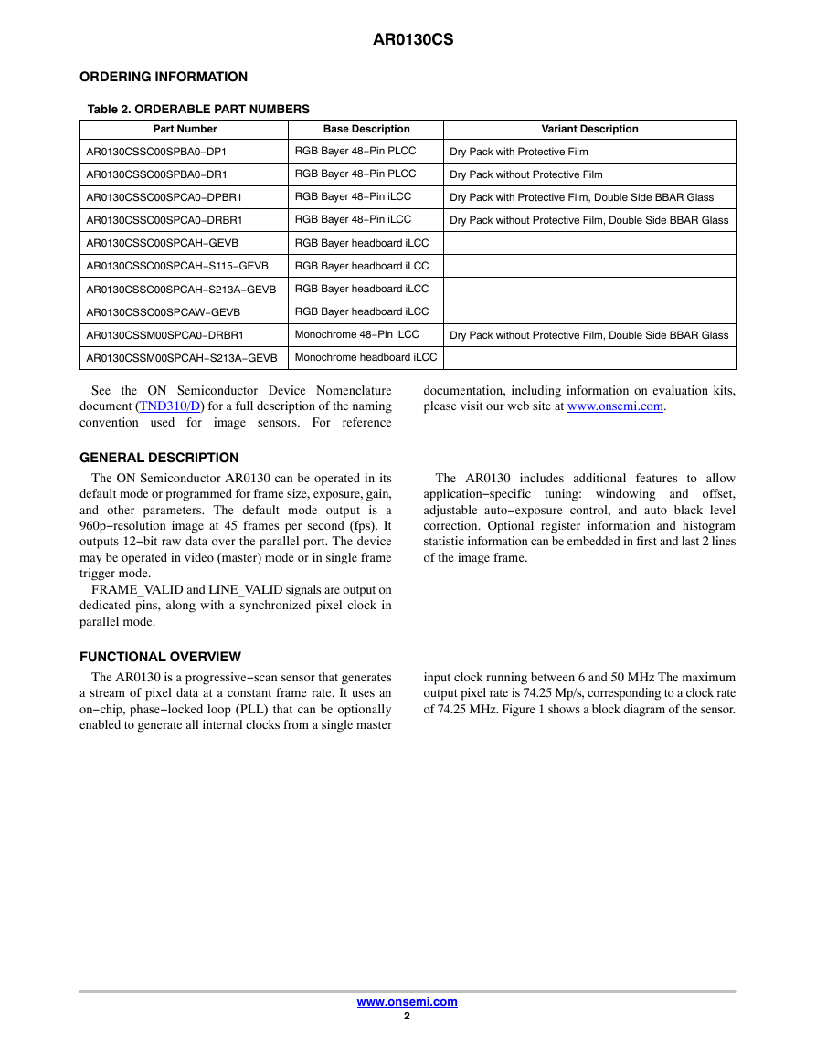
ORDERING INFORMATION
Table 2. ORDERABLE PART NUMBERS
Part Number
Base Description
Variant Description
AR0130CSSC00SPBA0−DP1
RGB Bayer 48−Pin PLCC
Dry Pack with Protective Film
AR0130CSSC00SPBA0−DR1
RGB Bayer 48−Pin PLCC
Dry Pack without Protective Film
AR0130CSSC00SPCA0−DPBR1
RGB Bayer 48−Pin iLCC
Dry Pack with Protective Film, Double Side BBAR Glass
AR0130CSSC00SPCA0−DRBR1
RGB Bayer 48−Pin iLCC
Dry Pack without Protective Film, Double Side BBAR Glass
AR0130CSSC00SPCAH−GEVB
RGB Bayer headboard iLCC
AR0130CSSC00SPCAH−S115−GEVB
RGB Bayer headboard iLCC
AR0130CSSC00SPCAH−S213A−GEVB
RGB Bayer headboard iLCC
AR0130CSSC00SPCAW−GEVB
RGB Bayer headboard iLCC
AR0130CSSM00SPCA0−DRBR1
Monochrome 48−Pin iLCC
Dry Pack without Protective Film, Double Side BBAR Glass
AR0130CSSM00SPCAH−S213A−GEVB Monochrome headboard iLCC
See the ON Semiconductor Device Nomenclature
document (TND310/D) for a full description of the naming
convention used for
image sensors. For reference
GENERAL DESCRIPTION
The ON Semiconductor AR0130 can be operated in its
default mode or programmed for frame size, exposure, gain,
and other parameters. The default mode output is a
960p−resolution image at 45 frames per second (fps). It
outputs 12−bit raw data over the parallel port. The device
may be operated in video (master) mode or in single frame
trigger mode.
FRAME_VALID and LINE_VALID signals are output on
dedicated pins, along with a synchronized pixel clock in
parallel mode.
FUNCTIONAL OVERVIEW
The AR0130 is a progressive−scan sensor that generates
a stream of pixel data at a constant frame rate. It uses an
on−chip, phase−locked loop (PLL) that can be optionally
enabled to generate all internal clocks from a single master
documentation, including information on evaluation kits,
please visit our web site at www.onsemi.com.
The AR0130 includes additional features to allow
application−specific
tuning: windowing and offset,
adjustable auto−exposure control, and auto black level
correction. Optional register information and histogram
statistic information can be embedded in first and last 2 lines
of the image frame.
input clock running between 6 and 50 MHz The maximum
output pixel rate is 74.25 Mp/s, corresponding to a clock rate
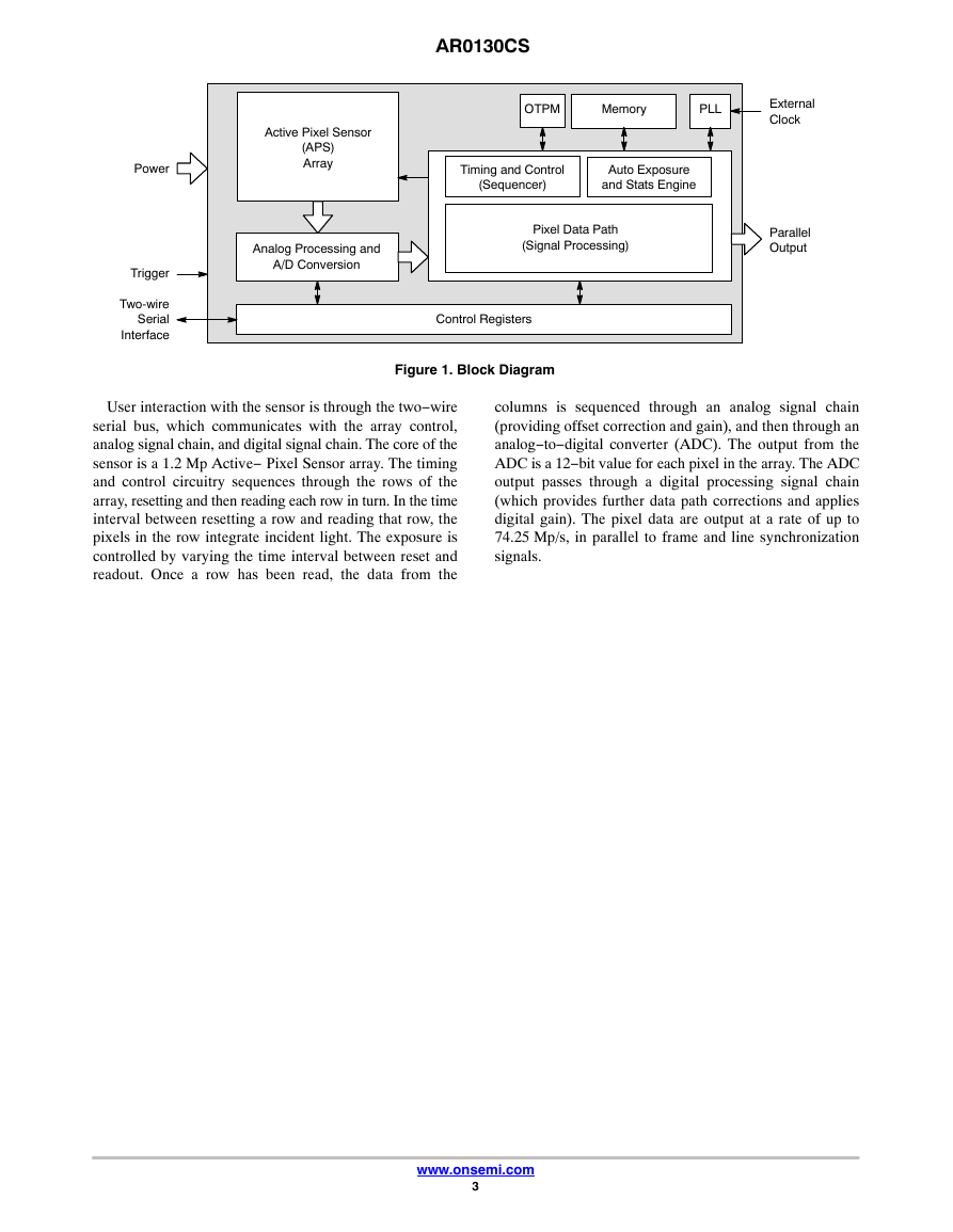
of 74.25 MHz. Figure 1 shows a block diagram of the sensor.
www.onsemi.com
2
�
AR0130CS
Active Pixel Sensor
(APS)
Array
Analog Processing and
A/D Conversion
OTPM
Memory
PLL
External
Clock
Timing and Control
(Sequencer)
Auto Exposure
and Stats Engine
Pixel Data Path
(Signal Processing)
Parallel
Output
Control Registers
Figure 1. Block Diagram
Power
Trigger
Two-wire
Serial
Interface
User interaction with the sensor is through the two−wire
serial bus, which communicates with the array control,
analog signal chain, and digital signal chain. The core of the
sensor is a 1.2 Mp Active− Pixel Sensor array. The timing
and control circuitry sequences through the rows of the
array, resetting and then reading each row in turn. In the time
interval between resetting a row and reading that row, the
pixels in the row integrate incident light. The exposure is
controlled by varying the time interval between reset and
readout. Once a row has been read, the data from the
columns is sequenced through an analog signal chain
(providing offset correction and gain), and then through an
analog−to−digital converter (ADC). The output from the
ADC is a 12−bit value for each pixel in the array. The ADC
output passes through a digital processing signal chain
(which provides further data path corrections and applies
digital gain). The pixel data are output at a rate of up to
74.25 Mp/s, in parallel to frame and line synchronization
signals.
www.onsemi.com
3
�
AR0130CS
Digital
I/O
Power1
Digital
Core
Power1
PLL
Power1
Analog
Power1
Analog
Power1
VDD_IO VDD
VDD_PLL
VAA VAA_PIX
DOUT [11:0]
PIXCLK
LINE_VALID
FRAME_VALID
To Controller
EXTCLK
SADDR
SDATA
SCLK
TRIGGER
OE_BAR
STANDBY
RESET_BAR
Reserved
2
W
k
5
.
1
3
,
2
W
k
5
.
1
Master Clock
(6 − 50 MHz)
From Controller
VDD_IO
VDD
VDD_PLL
VAA
VAA_PIX
DGND
AGND
Digital
Ground
Analog
Ground
Notes:
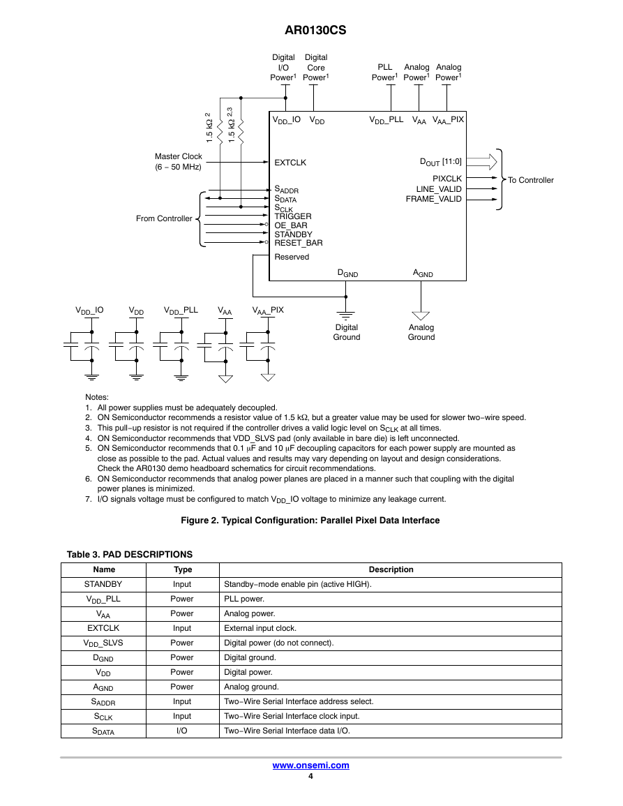
1. All power supplies must be adequately decoupled.
2. ON Semiconductor recommends a resistor value of 1.5 kW, but a greater value may be used for slower two−wire speed.
3. This pull−up resistor is not required if the controller drives a valid logic level on SCLK at all times.
4. ON Semiconductor recommends that VDD_SLVS pad (only available in bare die) is left unconnected.
5. ON Semiconductor recommends that 0.1 mF and 10 mF decoupling capacitors for each power supply are mounted as
close as possible to the pad. Actual values and results may vary depending on layout and design considerations.
Check the AR0130 demo headboard schematics for circuit recommendations.
6. ON Semiconductor recommends that analog power planes are placed in a manner such that coupling with the digital
power planes is minimized.
I/O signals voltage must be configured to match VDD_IO voltage to minimize any leakage current.
7.
Figure 2. Typical Configuration: Parallel Pixel Data Interface
Table 3. PAD DESCRIPTIONS
Type
Name
STANDBY
VDD_PLL
VAA
EXTCLK
VDD_SLVS
DGND
VDD
AGND
SADDR
SCLK
SDATA
Input
Power
Power
Input
Power
Power
Power
Power
Input
Input
I/O
Standby−mode enable pin (active HIGH).
Description
PLL power.
Analog power.
External input clock.
Digital power (do not connect).
Digital ground.
Digital power.
Analog ground.
Two−Wire Serial Interface address select.
Two−Wire Serial Interface clock input.
Two−Wire Serial Interface data I/O.
www.onsemi.com
4
�
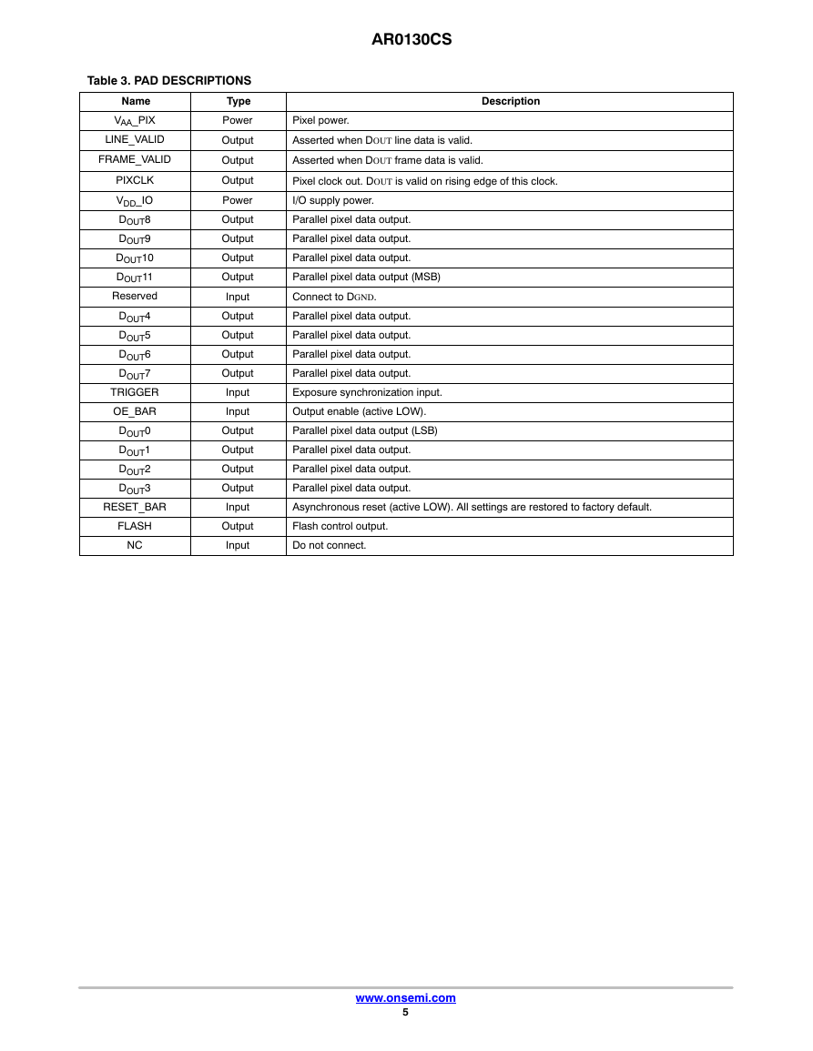
Table 3. PAD DESCRIPTIONS
Type
Name
VAA_PIX
LINE_VALID
FRAME_VALID
PIXCLK
VDD_IO
DOUT8
DOUT9
DOUT10
DOUT11
Reserved
DOUT4
DOUT5
DOUT6
DOUT7
TRIGGER
OE_BAR
DOUT0
DOUT1
DOUT2
DOUT3
RESET_BAR
FLASH
NC
Power
Output
Output
Output
Power
Output
Output
Output
Output
Input
Output
Output
Output
Output
Input
Input
Output
Output
Output
Output
Input
Output
Input
AR0130CS
Description
Pixel power.
Asserted when DOUT line data is valid.
Asserted when DOUT frame data is valid.
Pixel clock out. DOUT is valid on rising edge of this clock.
I/O supply power.
Parallel pixel data output.
Parallel pixel data output.
Parallel pixel data output.
Parallel pixel data output (MSB)
Connect to DGND.
Parallel pixel data output.
Parallel pixel data output.
Parallel pixel data output.
Parallel pixel data output.
Exposure synchronization input.
Output enable (active LOW).
Parallel pixel data output (LSB)
Parallel pixel data output.
Parallel pixel data output.
Parallel pixel data output.
Asynchronous reset (active LOW). All settings are restored to factory default.
Flash control output.
Do not connect.
www.onsemi.com
5
�
AR0130CS
K
L
C
T
X
E
D
N
G
D
L
L
P
_
D
D
V
6
T
U
O
D
5
T
U
O
D
4
T
U
O
D
3
T
U
O
D
2
T
U
O
D
1
T
U
O
D
0
T
U
O
D
D
N
G
D
C
N
6
5
4
3
2
1
48
47
46
45
44
43
7
8
9
10
11
12
13
14
15
16
17
18
42
41
40
39
38
37
36
35
34
33
32
31
NC
NC
VAA
AGND
VAA_PIX
VAA_PIX
VAA
AGND
VAA
NC
NC
NC
19
20
21
22
23
24
25
26
27
28
29
30
DOUT7
DOUT8
DOUT9
DOUT10
DOUT11
VDD_IO
PIXCLK
VDD
SCLK
SDATA
RESET_BAR
VDD_IO
C
N
C
N
D
D
V
Y
B
D
N
A
T
S
R
A
B
_
E
O
R
D
D
A
S
H
S
A
L
F
R
E
G
G
R
T
I
D
E
V
R
E
S
E
R
I
D
L
A
V
_
E
M
A
R
F
D
N
G
D
I
D
L
A
V
_
E
N
L
I
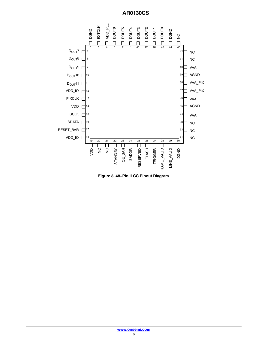
Figure 3. 48−Pin iLCC Pinout Diagram
www.onsemi.com
6
�
VDD_IO
VDD_IO
SCLK
SADDR
EXTCLK
PIXCLK
FLASH
SDATA
FRAME_VALID
LINE_VALID
DOUT11
DOUT10
AR0130CS
D
N
G
D
D
N
G
D
D
D
V
D
D
V
D
N
G
D
L
L
P
_
D
D
V
D
N
G
A
D
N
G
A
A
A
V
A
A
V
A
A
V
D
N
G
A
9
T
U
O
D
8
T
U
O
D
7
T
U
O
D
6
T
U
O
D
5
T
U
O
D
4
T
U
O
D
3
T
U
O
D
2
T
U
O
D
1
T
U
O
D
0
T
U
O
D
Top View
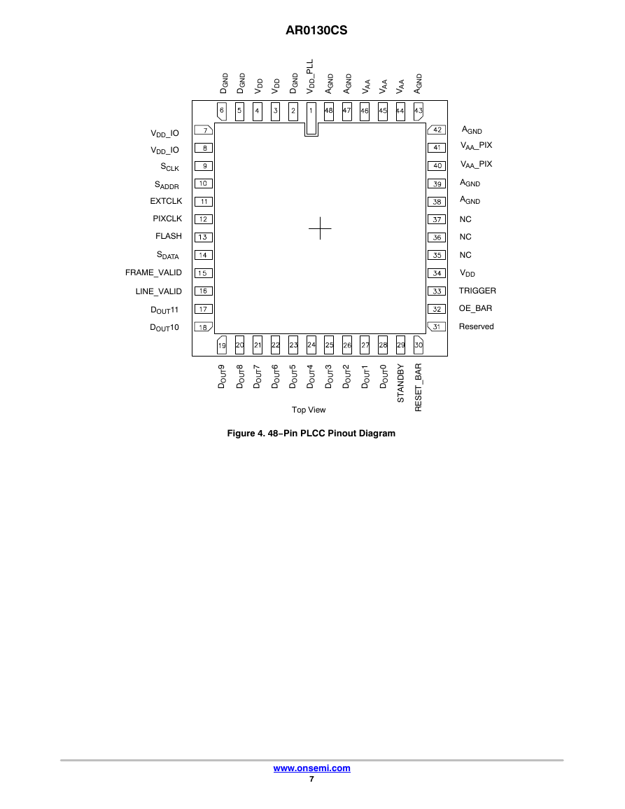
Figure 4. 48−Pin PLCC Pinout Diagram
Y
B
D
N
A
T
S
R
A
B
_
T
E
S
E
R
AGND
VAA_PIX
VAA_PIX
AGND
AGND
NC
NC
NC
VDD
TRIGGER
OE_BAR
Reserved
www.onsemi.com
7
�
AR0130CS
PIXEL DATA FORMAT
Pixel Array Structure
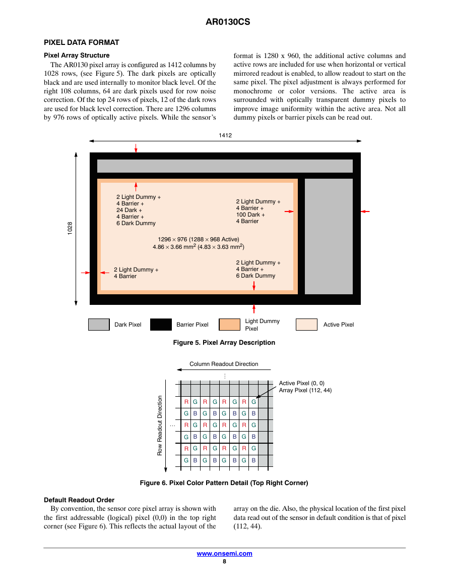
The AR0130 pixel array is configured as 1412 columns by
1028 rows, (see Figure 5). The dark pixels are optically
black and are used internally to monitor black level. Of the
right 108 columns, 64 are dark pixels used for row noise
correction. Of the top 24 rows of pixels, 12 of the dark rows
are used for black level correction. There are 1296 columns
by 976 rows of optically active pixels. While the sensor’s
format is 1280 x 960, the additional active columns and
active rows are included for use when horizontal or vertical
mirrored readout is enabled, to allow readout to start on the
same pixel. The pixel adjustment is always performed for
monochrome or color versions. The active area is
surrounded with optically transparent dummy pixels to
improve image uniformity within the active area. Not all
dummy pixels or barrier pixels can be read out.
1412
8
2
0
1
2 Light Dummy +
4 Barrier +
24 Dark +
4 Barrier +
6 Dark Dummy
2 Light Dummy +
4 Barrier +
100 Dark +
4 Barrier
1296 × 976 (1288 × 968 Active)
4.86 × 3.66 mm2 (4.83 × 3.63 mm2)
2 Light Dummy +
4 Barrier
2 Light Dummy +
4 Barrier +
6 Dark Dummy
Dark Pixel
Barrier Pixel
Light Dummy
Pixel
Active Pixel
Figure 5. Pixel Array Description
Active Pixel (0, 0)
Array Pixel (112, 44)
Column Readout Direction
…
G
B
G
B
G
B
R
G
R
G
R
G
G
B
G
B
G
B
R
G
R
G
R
G
G
B
G
B
G
B
…
R
G
R
G
R
G
G
B
G
B
G
B
R
G
R
G
R
G
n
o
i
t
c
e
r
i
D
t
u
o
d
a
e
R
w
o
R
Figure 6. Pixel Color Pattern Detail (Top Right Corner)
Default Readout Order
By convention, the sensor core pixel array is shown with
the first addressable (logical) pixel (0,0) in the top right
corner (see Figure 6). This reflects the actual layout of the
array on the die. Also, the physical location of the first pixel
data read out of the sensor in default condition is that of pixel
(112, 44).
www.onsemi.com
8
�



 2023年江西萍乡中考道德与法治真题及答案.doc
 2012年重庆南川中考生物真题及答案.doc
 2013年江西师范大学地理学综合及文艺理论基础考研真题.doc
 2020年四川甘孜小升初语文真题及答案I卷.doc
 2020年注册岩土工程师专业基础考试真题及答案.doc
 2023-2024学年福建省厦门市九年级上学期数学月考试题及答案.doc
 2021-2022学年辽宁省沈阳市大东区九年级上学期语文期末试题及答案.doc
 2022-2023学年北京东城区初三第一学期物理期末试卷及答案.doc
 2018上半年江西教师资格初中地理学科知识与教学能力真题及答案.doc
 2012年河北国家公务员申论考试真题及答案-省级.doc
 2020-2021学年江苏省扬州市江都区邵樊片九年级上学期数学第一次质量检测试题及答案.doc
 2022下半年黑龙江教师资格证中学综合素质真题及答案.doc