Preliminary
TTP229-LSF
TonTouchTM
16 KEYS OR 8 KEYS TOUCH PAD DETECTOR IC
GENERAL DESCRIPTION
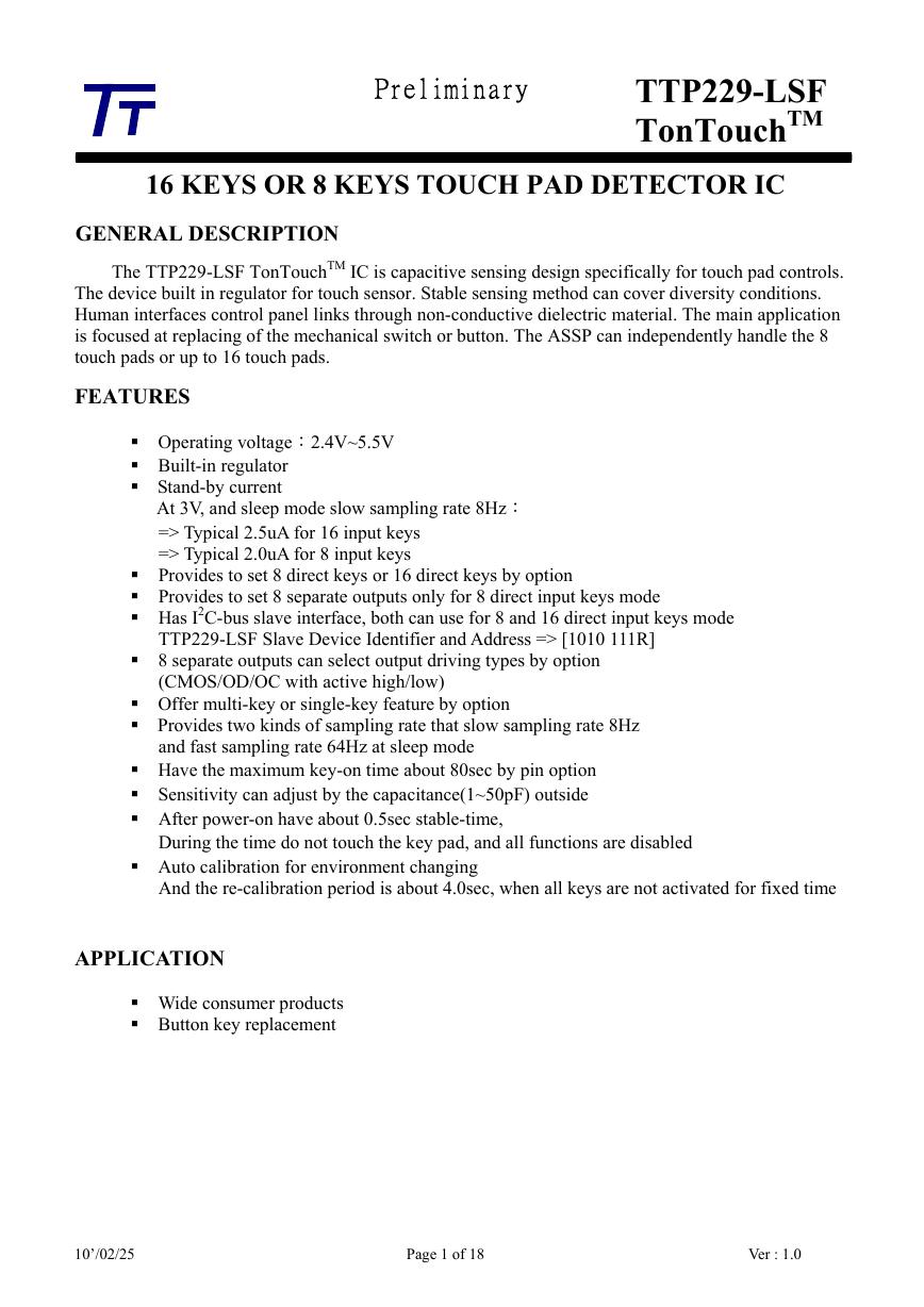
The TTP229-LSF TonTouchTM IC is capacitive sensing design specifically for touch pad controls.
The device built in regulator for touch sensor. Stable sensing method can cover diversity conditions.
Human interfaces control panel links through non-conductive dielectric material. The main application
is focused at replacing of the mechanical switch or button. The ASSP can independently handle the 8
touch pads or up to 16 touch pads.
FEATURES
Operating voltage:2.4V~5.5V
Built-in regulator
Stand-by current
At 3V, and sleep mode slow sampling rate 8Hz:
=> Typical 2.5uA for 16 input keys
=> Typical 2.0uA for 8 input keys
Provides to set 8 direct keys or 16 direct keys by option
Provides to set 8 separate outputs only for 8 direct input keys mode
Has I2C-bus slave interface, both can use for 8 and 16 direct input keys mode
TTP229-LSF Slave Device Identifier and Address => [1010 111R]
8 separate outputs can select output driving types by option
(CMOS/OD/OC with active high/low)
Offer multi-key or single-key feature by option
Provides two kinds of sampling rate that slow sampling rate 8Hz
and fast sampling rate 64Hz at sleep mode
Have the maximum key-on time about 80sec by pin option
Sensitivity can adjust by the capacitance(1~50pF) outside
After power-on have about 0.5sec stable-time,
During the time do not touch the key pad, and all functions are disabled
Auto calibration for environment changing
And the re-calibration period is about 4.0sec, when all keys are not activated for fixed time
APPLICATION
Wide consumer products
Button key replacement
10’/02/25 Page 1 of 18 Ver : 1.0
�
Preliminary
TTP229-LSF
TonTouchTM
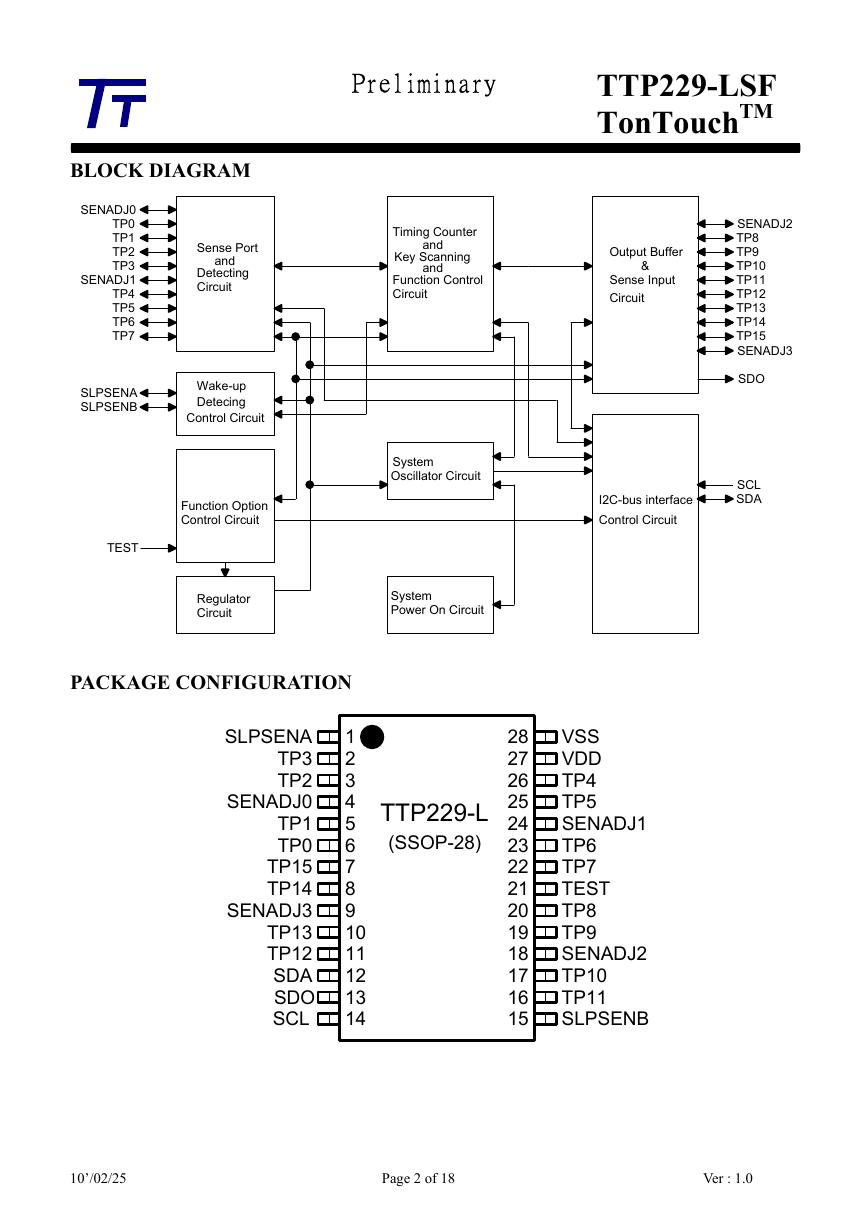
BLOCK DIAGRAM
SENADJ0
TP0
TP1
TP2
TP3
SENADJ1
TP4
TP5
TP6
TP7
SLPSENA
SLPSENB
Sense Port
and
Detecting
Circuit
Wake-up
Detecing
Control Circuit
Timing Counter
and
and
Key Scanning
Function Control
Circuit
Output Buffer
&
Sense Input
Circuit
SENADJ2
TP8
TP9
TP10
TP11
TP12
TP13
TP14
TP15
SENADJ3
SDO
Function Option
Control Circuit
TEST
System
Oscillator Circuit
I2C-bus interface
Control Circuit
SCL
SDA
Regulator
Circuit
System
Power On Circuit
PACKAGE CONFIGURATION
TTP229-L
(SSOP-28)
SLPSENA
TP3
TP2
SENADJ0
TP1
TP0
TP15
TP14
SENADJ3
TP13
TP12
SDA
SDO
SCL
1
2
3
4
5
6
7
8
9
10
11
12
13
14
28
27
26
25
24
23
22
21
20
19
18
17
16
15
VSS
VDD
TP4
TP5
SENADJ1
TP6
TP7
TEST
TP8
TP9
SENADJ2
TP10
TP11
SLPSENB
10’/02/25 Page 2 of 18 Ver : 1.0
�
Preliminary
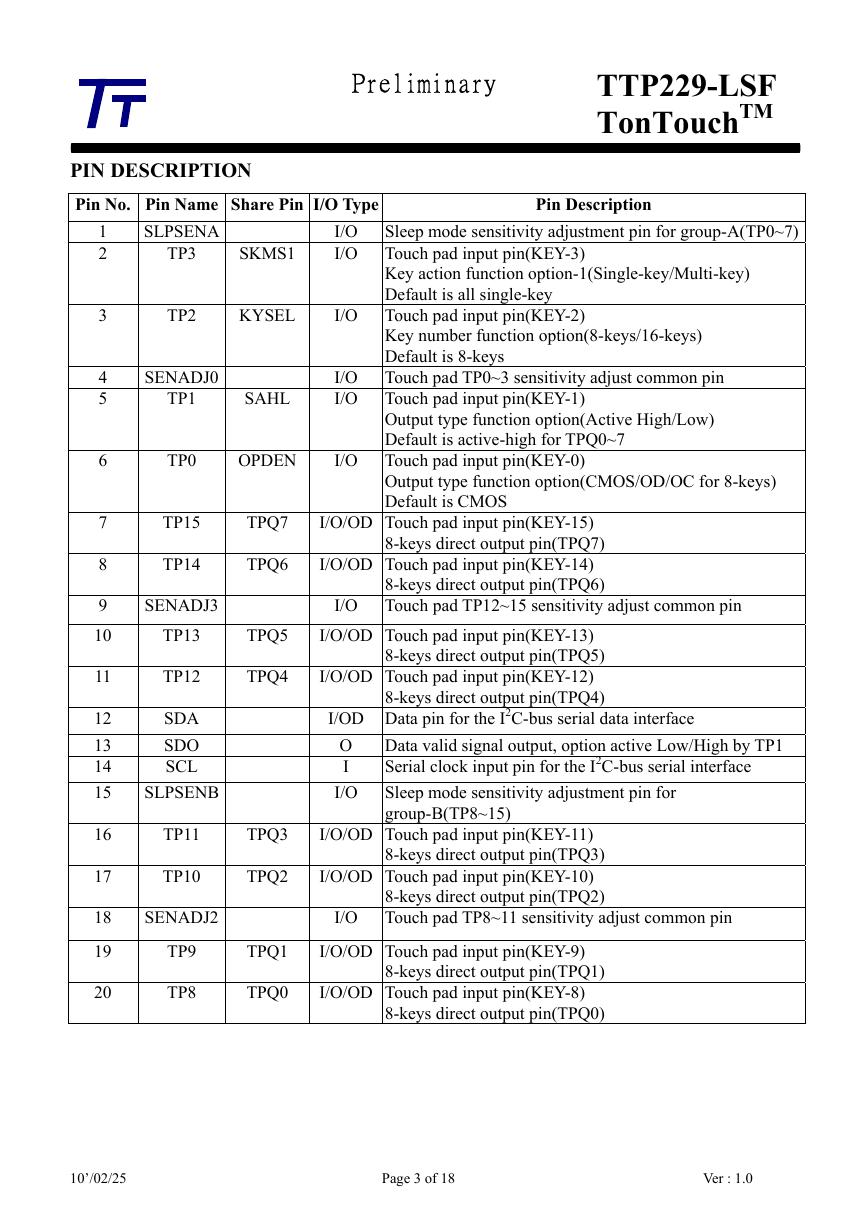
PIN DESCRIPTION
Pin No. Pin Name Share Pin I/O Type
TTP229-LSF
TonTouchTM
Pin Description
SLPSENA
TP3
SKMS1
I/O
I/O
TP2
KYSEL
I/O
SENADJ0
TP1
SAHL
I/O
I/O
TP0
OPDEN
I/O
Sleep mode sensitivity adjustment pin for group-A(TP0~7)
Touch pad input pin(KEY-3)
Key action function option-1(Single-key/Multi-key)
Default is all single-key
Touch pad input pin(KEY-2)
Key number function option(8-keys/16-keys)
Default is 8-keys
Touch pad TP0~3 sensitivity adjust common pin
Touch pad input pin(KEY-1)
Output type function option(Active High/Low)
Default is active-high for TPQ0~7
Touch pad input pin(KEY-0)
Output type function option(CMOS/OD/OC for 8-keys)
Default is CMOS
I/O/OD Touch pad input pin(KEY-15)
8-keys direct output pin(TPQ7)
I/O/OD Touch pad input pin(KEY-14)
8-keys direct output pin(TPQ6)
Touch pad TP12~15 sensitivity adjust common pin
I/O
I/O/OD Touch pad input pin(KEY-13)
8-keys direct output pin(TPQ5)
I/O/OD Touch pad input pin(KEY-12)
8-keys direct output pin(TPQ4)
I/OD Data pin for the I2C-bus serial data interface
O
I
I/O
Data valid signal output, option active Low/High by TP1
Serial clock input pin for the I2C-bus serial interface
Sleep mode sensitivity adjustment pin for
group-B(TP8~15)
I/O/OD Touch pad input pin(KEY-11)
8-keys direct output pin(TPQ3)
I/O/OD Touch pad input pin(KEY-10)
8-keys direct output pin(TPQ2)
Touch pad TP8~11 sensitivity adjust common pin
I/O
I/O/OD Touch pad input pin(KEY-9)
8-keys direct output pin(TPQ1)
I/O/OD Touch pad input pin(KEY-8)
8-keys direct output pin(TPQ0)
1
2
3
4
5
6
7
8
9
10
11
12
13
14
15
16
17
18
19
20
TP15
TP14
TPQ7
TPQ6
SENADJ3
TP13
TP12
SDA
SDO
SCL
SLPSENB
TPQ5
TPQ4
TP11
TP10
TPQ3
TPQ2
SENADJ2
TP9
TP8
TPQ1
TPQ0
10’/02/25 Page 3 of 18 Ver : 1.0
�
Preliminary
TTP229-LSF
TonTouchTM
Pin No. Pin Name Share Pin I/O Type
Pin Description
TEST
TP7
SKSRT
I-PL Only for test
I/O
21
22
23
24
25
26
27
28
TP6
SLWPTM
I/O
SENADJ1
TP5
WPSCT
I/O
I/O
TP4
SKMS0
I/O
VDD
VSS
P
P
Touch pad input pin(KEY-7)
Maximum key-on time function option(Infinite/80sec)
Default is infinite
Touch pad input pin(KEY-6)
Sleep mode sampling length function option(4.0/2.0mS)
Default is 4.0ms
Touch pad TP4~7 sensitivity adjust common pin
Touch pad input pin(KEY-5)
Sampling rate at sleep mode function option(8Hz/64Hz)
Default is 8Hz
Touch pad input pin(KEY-4)
Key action function option-0(Single-key/Multi-key)
Default is all single-key
Positive power supply
Negative power supply, ground
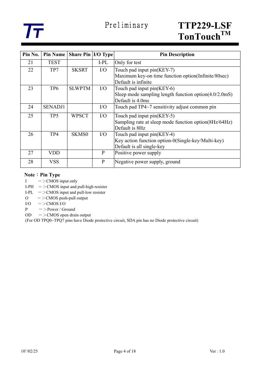
Note:Pin Type
I =>CMOS input only
I-PH =>CMOS input and pull-high resister
I-PL =>CMOS input and pull-low resister
O =>CMOS push-pull output
I/O =>CMOS I/O
P =>Power / Ground
OD =>CMOS open drain output
(For OD TPQ0~TPQ7 pins have Diode protective circuit, SDA pin has no Diode protective circuit)
10’/02/25 Page 4 of 18 Ver : 1.0
�
Preliminary
ELECTRICAL CHARACTERISTICS
‧Absolute Maximum Ratings
TTP229-LSF
TonTouchTM
Parameter
Operating Temperature
Storage Temperature
Power Supply Voltage
Input Voltage
Human Body Mode
Note:VSS symbolizes for system ground
Symbol
TOP
TSTG
VDD
VIN
ESD
Conditions
─
─
Ta=25°C
Ta=25°C
─
Value
-40 ~ +85
-50 ~ +125
VSS-0.3 ~ VSS+6.0
VSS-0.3 to VDD+0.3
6
Unit
℃
℃
V
V
KV
‧DC/AC Characteristics:(Test condition at room temperature=25℃)
Symbol
VDD
VREG
Test Condition
VDD=3.0V
IOP
ISD
VIL
VIH
IOL
IOH
TWU
TR
Set 8-Keys
Set 16-Keys
Set 8-Keys
Set 16-Keys
Sampling rate
8Hz
Sampling rate
64Hz
Input Low Voltage
Input High Voltage
VDD=3V, VOL=0.6V
VDD=3V, VOH=2.4V
VDD=3V, Sampling rate 8Hz
VDD=3V, Sampling rate 64Hz
VDD=3V, set 16-keys
VDD=3V, set 8-keys
TMOT
RPL VDD=3V,
Parameter
Operating Voltage
Internal Regulator Output
Operating Current
(no load)
Stand-by Current
(VDD=3.0V)
(Sampling length 4.0mS)
Input Ports
Input Ports
Output Port Sink Current
Output Port Source Current
Wake-up Response Time
(at sleep mode)
Output Response Time
(at operation)
Maximum Key-on Time
Input Pin Pull-low Resistor
(TEST)
Min. Typ. Max. Unit
V
2.4
2.2
V
uA
5.5
2.4
-
2.3
20
0
0.8
-
-
50
2.0
2.5
5.5
9.0
-
-
8
-4
125
15.6
32
16
80
30K
uA
0.2 VDD
1.0 VDD
-
mA
mA
-
mS
mS
mS
mS
110
Sec
ohm
10’/02/25 Page 5 of 18 Ver : 1.0
�
Preliminary
TTP229-LSF
TonTouchTM
FUNCTION DESCRIPTION
1. Sensitivity adjustment
The total loading of electrode size and capacitance of connecting line on PCB can affect the
sensitivity. So the sensitivity adjustment must according to the practical application on PCB. The
TTP229-LSF offers some methods for adjusting the sensitivity outside.
1-1 by the electrode size
Under other conditions are fixed. Using a larger electrode size can increase sensitivity. Otherwise
it can decrease sensitivity. But the electrode size must use in the effective scope.
1-2 by the panel thickness
Under other conditions are fixed. Using a thinner panel can increase sensitivity. Otherwise it can
decrease sensitivity. But the panel thickness must be below the maximum value.
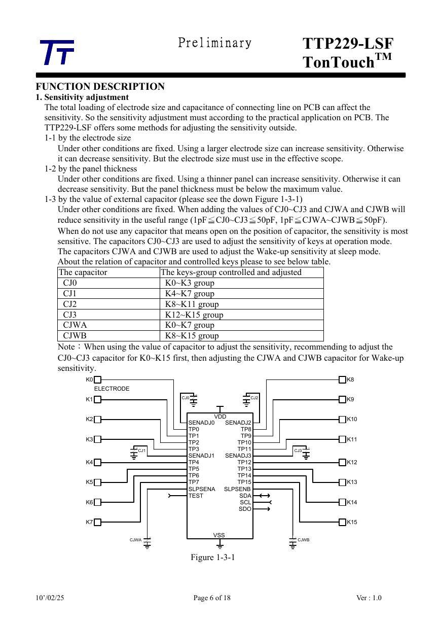
1-3 by the value of external capacitor (please see the down Figure 1-3-1)
Under other conditions are fixed. When adding the values of CJ0~CJ3 and CJWA and CJWB will
reduce sensitivity in the useful range (1pF≦CJ0~CJ3≦50pF, 1pF≦CJWA~CJWB≦50pF).
When do not use any capacitor that means open on the position of capacitor, the sensitivity is most
sensitive. The capacitors CJ0~CJ3 are used to adjust the sensitivity of keys at operation mode.
The capacitors CJWA and CJWB are used to adjust the Wake-up sensitivity at sleep mode.
About the relation of capacitor and controlled keys please to see below table.
The capacitor
CJ0
CJ1
CJ2
CJ3
CJWA
CJWB
Note:When using the value of capacitor to adjust the sensitivity, recommending to adjust the
CJ0~CJ3 capacitor for K0~K15 first, then adjusting the CJWA and CJWB capacitor for Wake-up
sensitivity.
K0
The keys-group controlled and adjusted
K0~K3 group
K4~K7 group
K8~K11 group
K12~K15 group
K0~K7 group
K8~K15 group
K8
ELECTRODE
CJ0
CJ2
CJ1
CJ3
VDD
SENADJ0
TP0
TP1
TP2
TP3
SENADJ1
TP4
TP5
TP6
TP7
SLPSENA
TEST
SENADJ2
TP8
TP9
TP10
TP11
SENADJ3
TP12
TP13
TP14
TP15
SLPSENB
SDA
SCL
SDO
K1
K2
K3
K4
K5
K6
K7
CJWA
VSS
CJWB
Figure 1-3-1
K9
K10
K11
K12
K13
K14
K15
10’/02/25 Page 6 of 18 Ver : 1.0
�
Preliminary
TTP229-LSF
TonTouchTM
2. Input keys number select
3. Output mode
The TTP229-LSF has 8 keys input mode and 16 keys input mode. These modes are selected via
high-value resistor connected to the TP2(KYSEL) pin to VSS, or not. The default that TP2(KYSEL) pin
is not used resistor connected to VSS is selected 8 keys input mode. Another is selected 16 keys input
mode that has used a high-value resistor connected to VSS.
The TTP229-LSF has 8 pins direct output mode and I2C-bus slave interface mode. The output of 16
keys input mode only offer I2C-bus slave interface. The 8 keys input mode has two kinds of output
that 8 pins direct output and I2C-bus slave interface. The 8 pins direct output only use at 8 keys input
mode.
3-1 At the 8 pins direct output mode, the TTP229-LSF has two kinds of output type that they are
CMOS type output and OD (Open Drain) type output. These are selected by the TP0(OPDEN) pin. The
CMOS type output is default that the TP0(OPDEN) pin is not used any component to VSS. When the
TP0(OPDEN) pin is used a high-value resistor connected to VSS, it is selected OD type output.
3-2 When selecting 8 pins direct CMOS output mode, the output channels can be set active-high or
active-low by TP1(SAHL) pin. The default that the TP1(SAHL) pin is not used a high-value resistor, it is
set active-high. When the TP1(SAHL) pin has a high-value resistor connected to VSS, it is set
active-low.
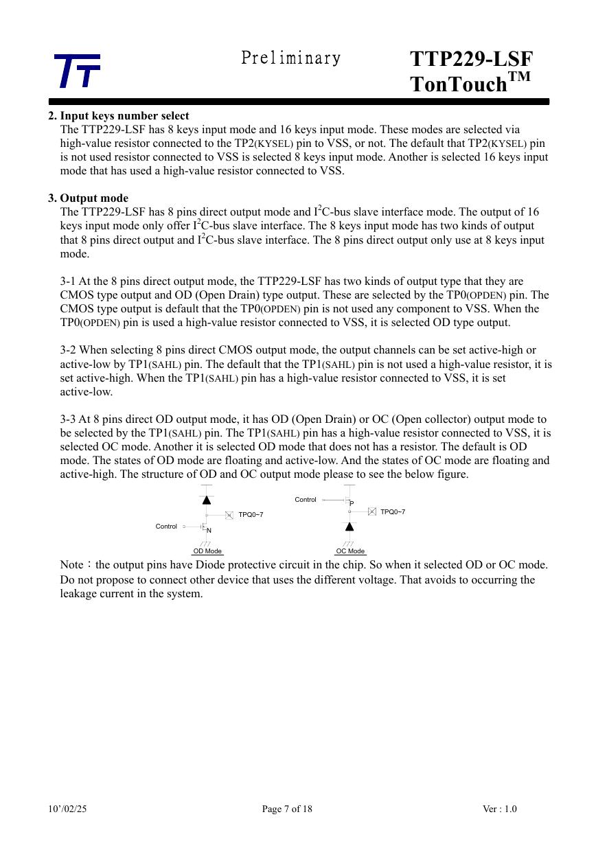
3-3 At 8 pins direct OD output mode, it has OD (Open Drain) or OC (Open collector) output mode to
be selected by the TP1(SAHL) pin. The TP1(SAHL) pin has a high-value resistor connected to VSS, it is
selected OC mode. Another it is selected OD mode that does not has a resistor. The default is OD
mode. The states of OD mode are floating and active-low. And the states of OC mode are floating and
active-high. The structure of OD and OC output mode please to see the below figure.
TPQ0~7
Control
P
TPQ0~7
Control
N
OD Mode
OC Mode
Note:the output pins have Diode protective circuit in the chip. So when it selected OD or OC mode.
Do not propose to connect other device that uses the different voltage. That avoids to occurring the
leakage current in the system.
10’/02/25 Page 7 of 18 Ver : 1.0
�
Preliminary
TTP229-LSF
TonTouchTM
3-4 At I2C-bus slave interface mode the SDA pin is a serial data pin, the SCL is a serial clock input
pin. The SDA and SCL pins must be pulled-high with an external resistor.
And the 4-bits identify code for the TTP229-LSF is〝 (1010) 〞. The device address for TTP229-LSF
B3~B1 bits are fixed 〝 111 〞. The TTP229-LSF 8-bits slave device address includes 4-bits identifier,
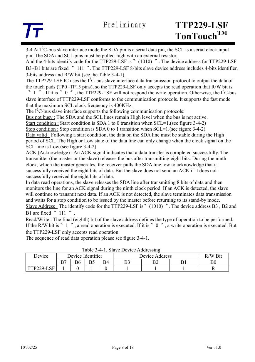
3-bits address and R/W bit (see the Table 3-4-1).
The TTP229-LSF IC uses the I2C-bus slave interface data transmission protocol to output the data of
the touch pads (TP0~TP15 pins), so the TTP229-LSF only accepts the read operation that R/W bit is
〝 1 〞. If it is〝 0 〞, the TTP229-LSF will not respond the write operation. Otherwise, the I2C-bus
slave interface of TTP229-LSF conforms to the communication protocols. It supports the fast mode
that the maximum SCL clock frequency is 400KHz.
The I2C-bus slave interface supports the following communication protocols:
Bus not busy : The SDA and the SCL lines remain High level when the bus is not active.
Start condition : Start condition is SDA 1 to 0 transition when SCL=1.(see figure 3-4-2)
Stop condition : Stop condition is SDA 0 to 1 transition when SCL=1.(see figure 3-4-2)
Data valid : Following a start condition, the data on the SDA line must be stable during the High
period of SCL. The High or Low state of the data line can only change when the clock signal on the
SCL line is Low.(see figure 3-4-2)
ACK (Acknowledge) : An ACK signal indicates that a data transfer is completed successfully. The
transmitter (the master or the slave) releases the bus after transmitting eight bits. During the ninth
clock, which the master generates, the receiver pulls the SDA line low to acknowledge that it
successfully received the eight bits of data. But the slave does not send an ACK if it does not
successfully received the eight bits of data.
In data read operations, the slave releases the SDA line after transmitting 8 bits of data and then
monitors the line for an ACK signal during the ninth clock period. If an ACK is detected, the slave
will continue to transmit next data. If an ACK is not detected, the slave terminates data transmission
and waits for a stop condition to be issued by the master before returning to its stand-by mode.
Slave Address : The identify code for the TTP229-LSF is〝 (1010) 〞. The device address B3 , B2 and
B1 are fixed〝 111 〞.
Read/Write : The final (eighth) bit of the slave address defines the type of operation to be performed.
If the R/W bit is〝 1 〞, a read operation is executed. If it is〝 0 〞, a write operation is executed. But
the TTP229-LSF only accepts read operation.
The sequence of read data operation please see figure 3-4-1.
Device
TTP229-LSF
Table 3-4-1. Slave Device Addressing
Device Identifier
Device Address
B7
1
B6
0
B5
1
B4
0
B3
1
B2
1
B1
1
R/W Bit
B0
R
10’/02/25 Page 8 of 18 Ver : 1.0
�



 V2版本原理图(Capacitive-Fingerprint-Reader-Schematic_V2).pdf
 摄像头工作原理.doc
 VL53L0X简要说明(En.FLVL53L00216).pdf
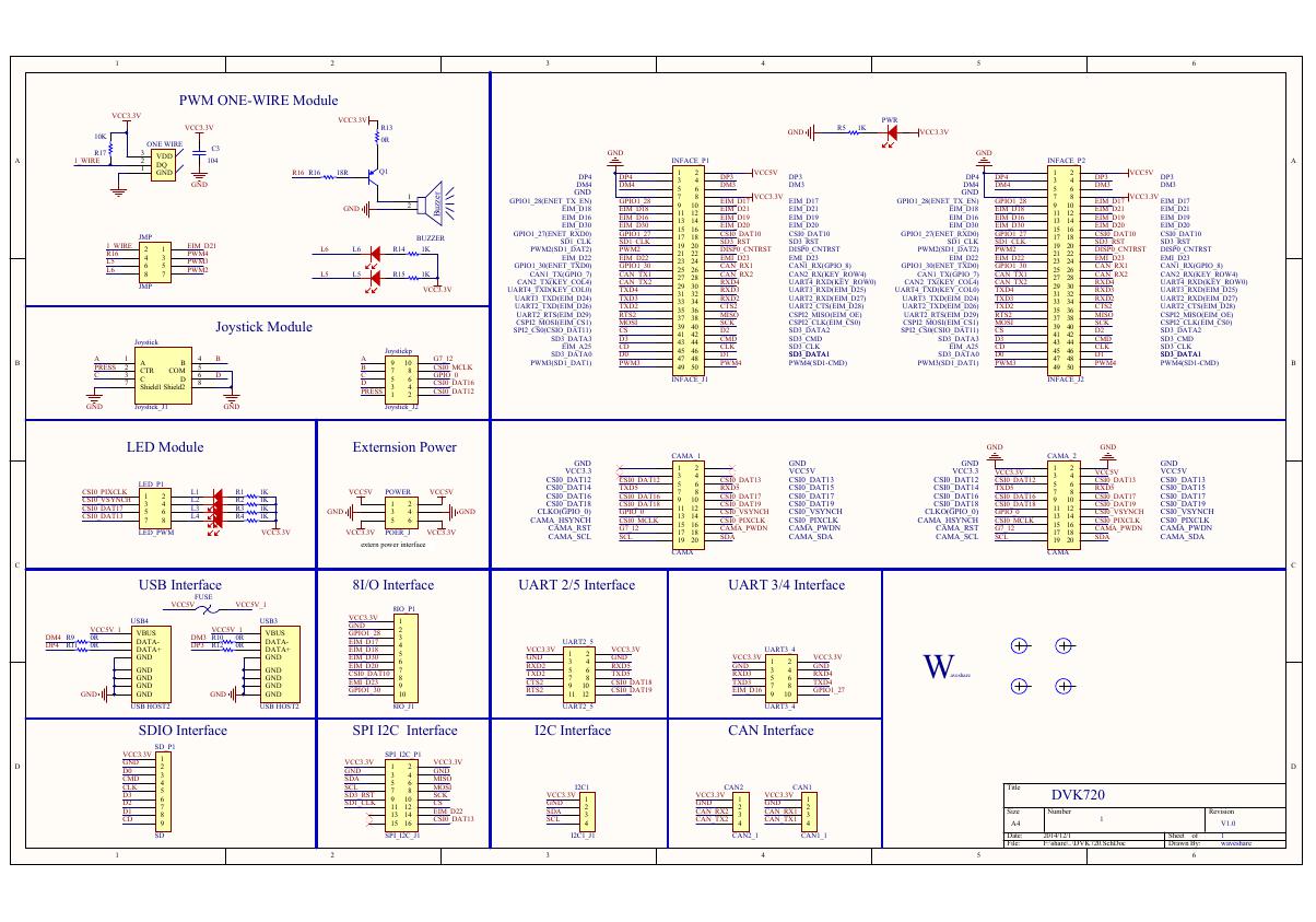 原理图(DVK720-Schematic).pdf
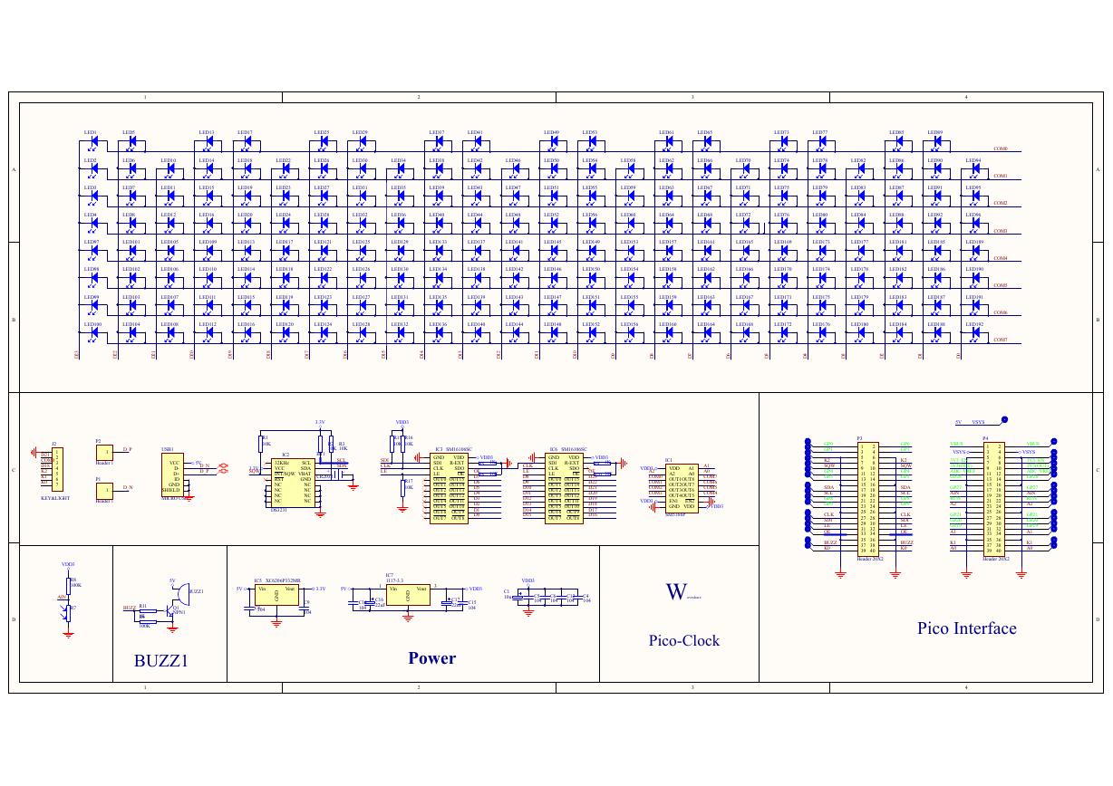 原理图(Pico-Clock-Green-Schdoc).pdf
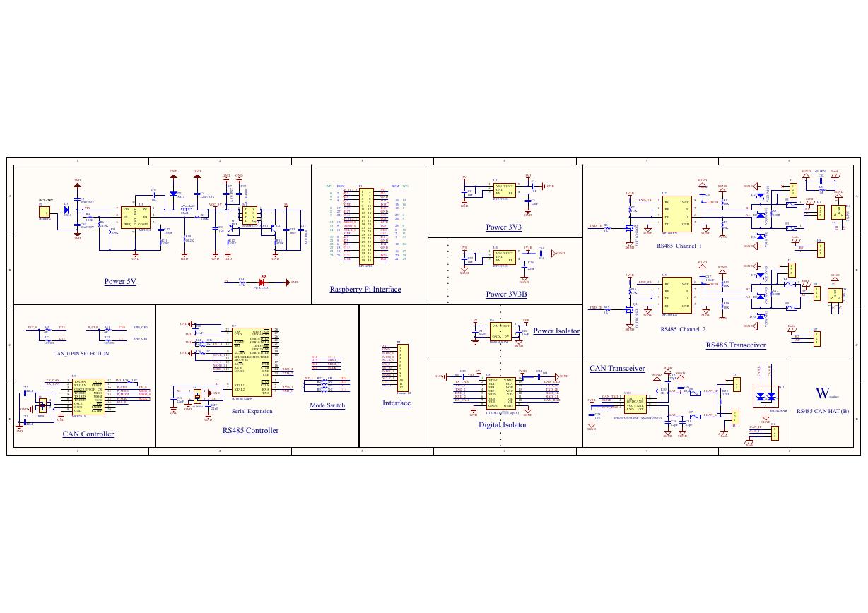 原理图(RS485-CAN-HAT-B-schematic).pdf
 File:SIM7500_SIM7600_SIM7800 Series_SSL_Application Note_V2.00.pdf
 ADS1263(Ads1262).pdf
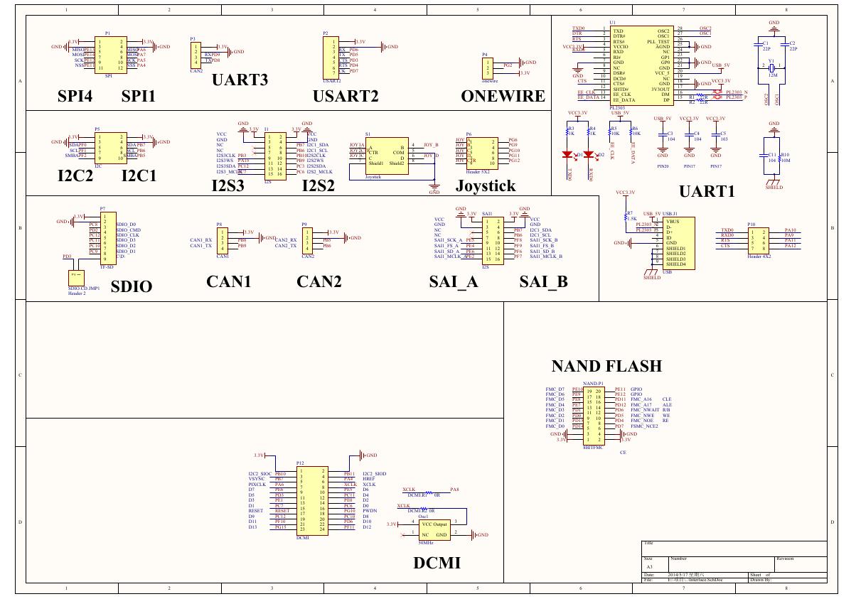 原理图(Open429Z-D-Schematic).pdf
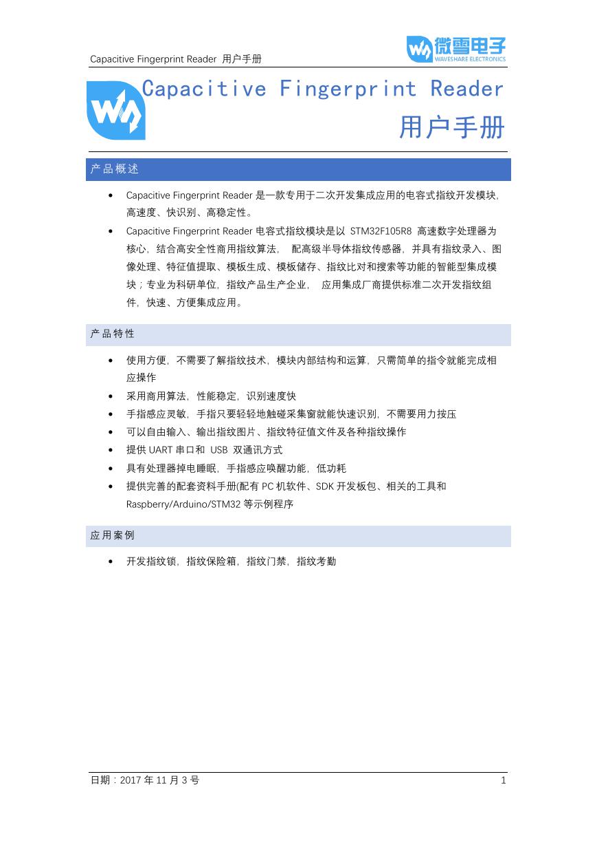 用户手册(Capacitive_Fingerprint_Reader_User_Manual_CN).pdf
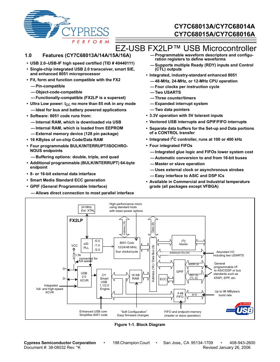 CY7C68013A(英文版)(CY7C68013A).pdf
 TechnicalReference_Dem.pdf