logo资料库

VL53L1X数据手册(VL53L1X).pdf

第1页 / 共35页
第2页 / 共35页
第3页 / 共35页
第4页 / 共35页
第5页 / 共35页
第6页 / 共35页
第7页 / 共35页
第8页 / 共35页
资料共35页,剩余部分请下载后查看
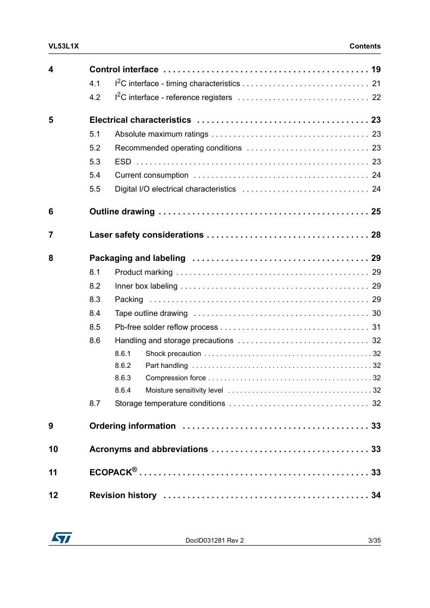
1 Product overview
1.1 Technical specification
Table 1. Technical specification
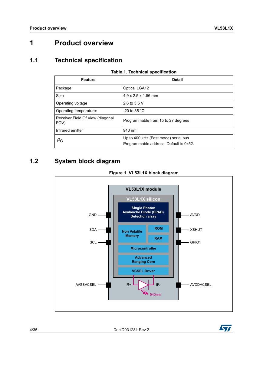
1.2 System block diagram
Figure 1. VL53L1X block diagram
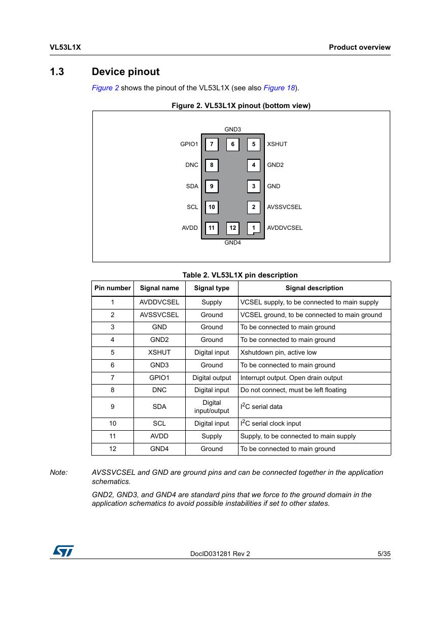
1.3 Device pinout
Figure 2. VL53L1X pinout (bottom view)
Table 2. VL53L1X pin description
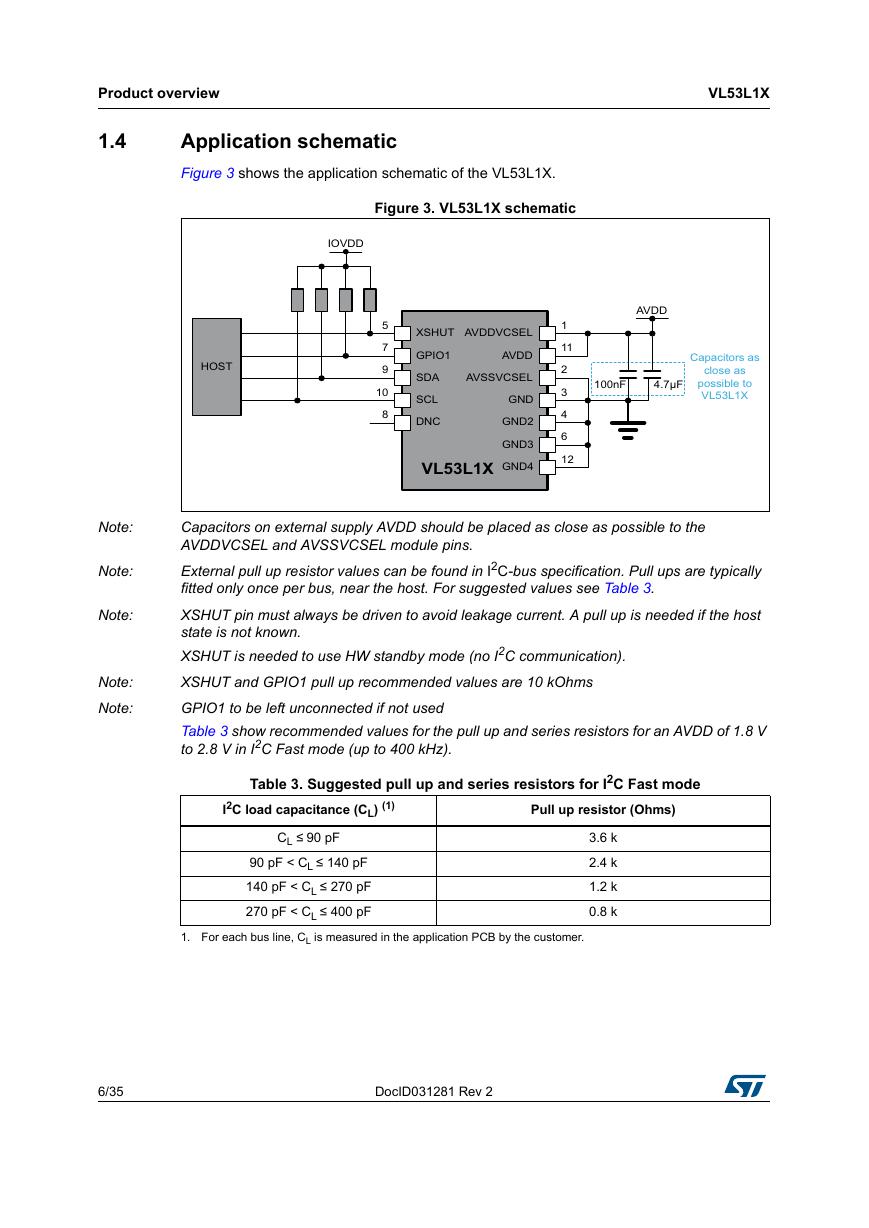
1.4 Application schematic
Figure 3. VL53L1X schematic
Table 3. Suggested pull up and series resistors for I2C Fast mode
2 Functional description
2.1 System functional description
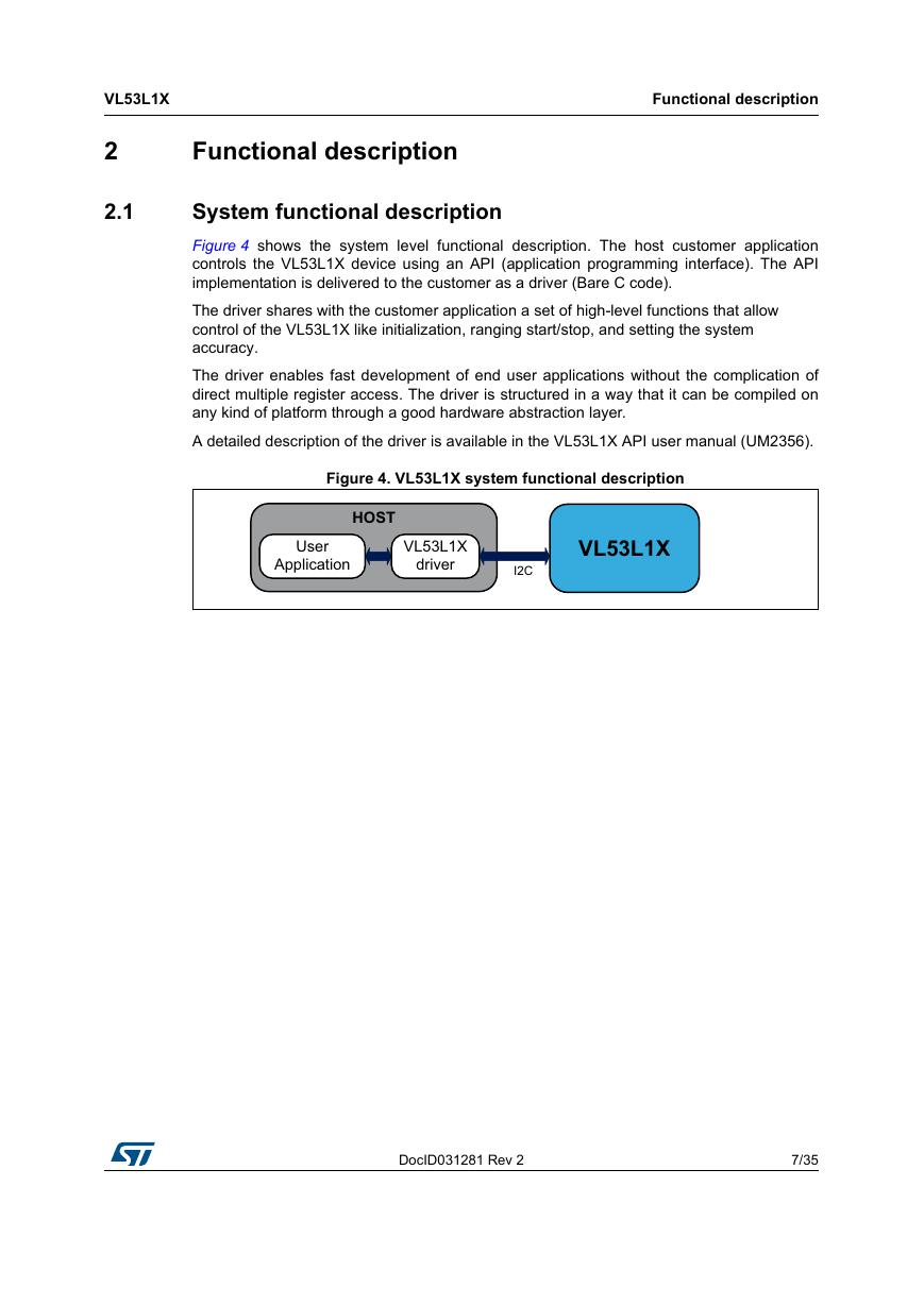
Figure 4. VL53L1X system functional description
2.2 System state machine description
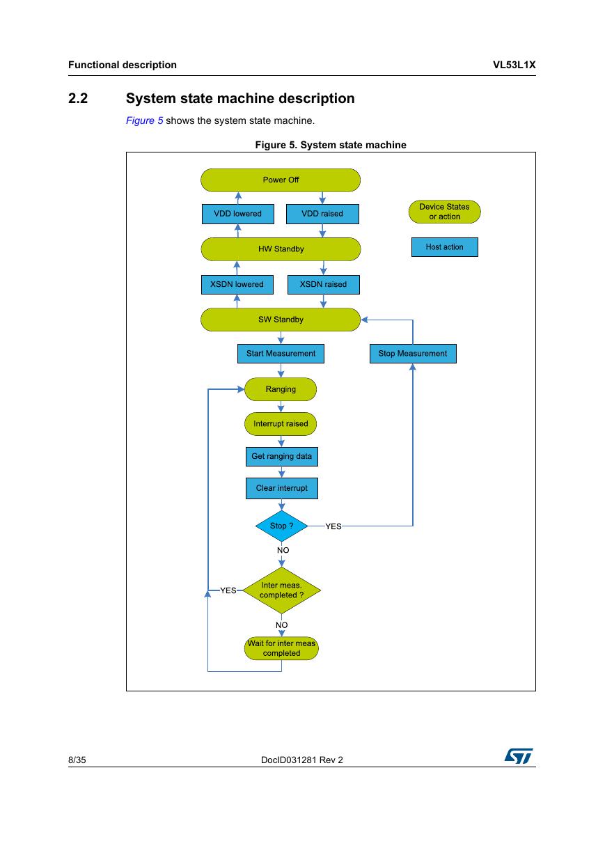
Figure 5. System state machine
2.3 Customer manufacturing calibration flow
2.4 Ranging description
2.5 Key parameters
2.5.1 Distance mode
Table 4. Maximum distance vs. Distance mode under ambient light
2.5.2 Timing budget (TB)
Figure 6. Maximum distance and repeatability error vs. timing budget
2.6 Power sequence
2.6.1 Power up and boot sequence
Figure 7. Power up and boot sequence
Figure 8. Power up and boot sequence with XSHUT not controlled
2.7 Ranging sequences
Figure 9. Autonomous sequence
2.8 Sensing array optical center
Table 5. Optical center specification
Figure 10. Optical center specification
3 Ranging performances
3.1 Test conditions
3.2 Accuracy, repeatability, and ranging error definitions
3.2.1 Accuracy definition
3.2.2 Repeatability definition
3.2.3 Ranging error definition
3.3 Minimum ranging distance
3.4 Performances in dark conditions
Table 6. Performances in dark conditions
3.5 Performances in ambient light conditions
3.5.1 Long distance mode
Table 7. Typical performances in ambient light with long distance mode
3.5.2 Short distance mode
Table 8. Typical performances in ambient light conditions with short distance mode
3.6 Performances in partial ROI in dark conditions
Table 9. Typical performances in partial ROI in dark conditions
4 Control interface
Figure 11. Data transfer protocol
Figure 12. VL53L1X I2C device address: 0x52
Figure 13. VL53L1X data format (write)
Figure 14. VL53L1X data format (read)
Figure 15. VL53L1X data format (sequential write)
Figure 16. VL53L1X data format (sequential read)
4.1 I2C interface - timing characteristics
Table 10. I2C interface - timing characteristics for Fast mode (400 kHz)
Figure 17. I2C timing characteristics
4.2 I2C interface - reference registers
Table 11. Reference registers
Table 12. 32-bit register example
5 Electrical characteristics
5.1 Absolute maximum ratings
Table 13. Absolute maximum ratings
5.2 Recommended operating conditions
Table 14. Recommended operating conditions
5.3 ESD
Table 15. ESD performances
5.4 Current consumption
Table 16. Power consumption at ambient temperature
5.5 Digital I/O electrical characteristics
Table 17. Digital I/O electrical characteristics
6 Outline drawing
Figure 18. Outline drawing (page 1/3)
Figure 19. Outline drawing (page 2/3)
Figure 20. Outline drawing (page 3/3
7 Laser safety considerations
Figure 21. Class 1 laser product label
8 Packaging and labeling
8.1 Product marking
Figure 22. Example of prototype marking
8.2 Inner box labeling
8.3 Packing
8.4 Tape outline drawing
Figure 23. Tape outline drawing
8.5 Pb-free solder reflow process
Table 18. Recommended solder profile
Figure 24. Solder profile
8.6 Handling and storage precautions
8.6.1 Shock precaution
8.6.2 Part handling
8.6.3 Compression force
8.6.4 Moisture sensitivity level
8.7 Storage temperature conditions
Table 19. Recommended storage conditions
9 Ordering information
Table 20. Order codes
10 Acronyms and abbreviations
Table 21. Acronyms and abbreviations
11 ECOPACK®
12 Revision history
Table 22. Document revision history
VL53L1X A new generation, long distance ranging Time-of-Flight sensor based on ST’s FlightSense™ technology Datasheet - production data Applications • User detection (Autonomous low-power mode) to power on/off and lock/unlock devices like personal computers/laptops and the IoT • Service robots and vacuum cleaners (long distance and fast obstacle detection) • Drones (landing assistance, hovering, ceiling detection) • Smart shelves and vending machines (goods inventory monitoring) • Sanitary (robust user detection whatever the target reflectance) • Smart building and smart lighting (people detection, gesture control) • 1 D gesture recognition • Laser assisted autofocus which enhances the camera autofocus system speed and robustness, especially in difficult scenes (low light and low contrast) and video focus tracking assistance Description The VL53L1X is a state-of-the-art, Time-of-Flight (ToF), laser-ranging sensor, enhancing the ST FlightSense™ product family. It is the fastest miniature ToF sensor on the market with accurate ranging up to 4 m and fast ranging frequency up to 50 Hz Housed in a miniature and reflowable package, it integrates a SPAD receiving array, a 940 nm invisible Class1 laser emitter, physical infrared filters, and optics to achieve the best ranging performance in various ambient lighting conditions with a range of cover window options. Unlike conventional IR sensors, the VL53L1X uses ST’s latest generation ToF technology which allows absolute distance measurement whatever the target color and reflectance. It is also possible to program the size of the ROI on the receiving array, allowing the sensor FoV to be reduced. Features • Fully integrated miniature module – Size: 4.9x2.5x1.56 mm – Emitter: 940 nm invisible laser (Class1) – SPAD (single photon avalanche diode) receiving array with integrated lens – Low-power microcontroller running advanced digital firmware • Pin-to-pin compatible with the VL53L0X FlightSense™ ranging sensor • Fast and accurate long distance ranging – Up to 400 cm distance measurement – Up to 50 Hz ranging frequency • Typical full field-of-view (FoV): 27 ° • Programmable region-of-interest (ROI) size on the receiving array, allowing the sensor FoV to be reduced • Programmable ROI position on the receiving array, providing multizone operation control from the host • Easy integration – Single reflowable component – Can be hidden behind many cover window materials – Software driver and code examples for turnkey ranging – Single power supply (2v8) – I²C interface (up to 1 MHz) – Shutdown and interrupt pins February 2018 This is information on a product in full production. DocID031281 Rev 2 1/35 www.st.com
Contents Contents VL53L1X 1 2 3 Product overview . . . . . . . . . . . . . . . . . . . . . . . . . . . . . . . . . . . . . . . . . . . 4 Technical specification . . . . . . . . . . . . . . . . . . . . . . . . . . . . . . . . . . . . . . . . 4 1.1 1.2 System block diagram . . . . . . . . . . . . . . . . . . . . . . . . . . . . . . . . . . . . . . . . 4 Device pinout . . . . . . . . . . . . . . . . . . . . . . . . . . . . . . . . . . . . . . . . . . . . . . . 5 1.3 1.4 Application schematic . . . . . . . . . . . . . . . . . . . . . . . . . . . . . . . . . . . . . . . . . 6 Functional description . . . . . . . . . . . . . . . . . . . . . . . . . . . . . . . . . . . . . . . 7 2.1 System functional description . . . . . . . . . . . . . . . . . . . . . . . . . . . . . . . . . . . 7 System state machine description . . . . . . . . . . . . . . . . . . . . . . . . . . . . . . . 8 2.2 Customer manufacturing calibration flow . . . . . . . . . . . . . . . . . . . . . . . . . . 9 2.3 2.4 Ranging description . . . . . . . . . . . . . . . . . . . . . . . . . . . . . . . . . . . . . . . . . . 9 Key parameters . . . . . . . . . . . . . . . . . . . . . . . . . . . . . . . . . . . . . . . . . . . . 10 2.5 Distance mode . . . . . . . . . . . . . . . . . . . . . . . . . . . . . . . . . . . . . . . . . . . . 10 2.5.1 2.5.2 Timing budget (TB) . . . . . . . . . . . . . . . . . . . . . . . . . . . . . . . . . . . . . . . . 11 Power sequence . . . . . . . . . . . . . . . . . . . . . . . . . . . . . . . . . . . . . . . . . . . . 12 2.6.1 Power up and boot sequence . . . . . . . . . . . . . . . . . . . . . . . . . . . . . . . . 12 Ranging sequences . . . . . . . . . . . . . . . . . . . . . . . . . . . . . . . . . . . . . . . . . 13 Sensing array optical center . . . . . . . . . . . . . . . . . . . . . . . . . . . . . . . . . . . 14 2.7 2.8 2.6 Ranging performances . . . . . . . . . . . . . . . . . . . . . . . . . . . . . . . . . . . . . . 15 Test conditions . . . . . . . . . . . . . . . . . . . . . . . . . . . . . . . . . . . . . . . . . . . . . 15 3.1 3.2 Accuracy, repeatability, and ranging error definitions . . . . . . . . . . . . . . . . 16 Accuracy definition . . . . . . . . . . . . . . . . . . . . . . . . . . . . . . . . . . . . . . . . . 16 3.2.1 Repeatability definition . . . . . . . . . . . . . . . . . . . . . . . . . . . . . . . . . . . . . . 16 3.2.2 3.2.3 Ranging error definition . . . . . . . . . . . . . . . . . . . . . . . . . . . . . . . . . . . . . 16 Minimum ranging distance . . . . . . . . . . . . . . . . . . . . . . . . . . . . . . . . . . . . 16 Performances in dark conditions . . . . . . . . . . . . . . . . . . . . . . . . . . . . . . . 16 Performances in ambient light conditions . . . . . . . . . . . . . . . . . . . . . . . . . 17 Long distance mode . . . . . . . . . . . . . . . . . . . . . . . . . . . . . . . . . . . . . . . 17 3.5.1 3.5.2 Short distance mode . . . . . . . . . . . . . . . . . . . . . . . . . . . . . . . . . . . . . . . 17 Performances in partial ROI in dark conditions . . . . . . . . . . . . . . . . . . . . 18 3.3 3.4 3.5 3.6 2/35 DocID031281 Rev 2
VL53L1X Contents 4 5 6 7 8 9 10 11 12 Control interface . . . . . . . . . . . . . . . . . . . . . . . . . . . . . . . . . . . . . . . . . . . 19 I2C interface - timing characteristics . . . . . . . . . . . . . . . . . . . . . . . . . . . . . 21 4.1 I2C interface - reference registers . . . . . . . . . . . . . . . . . . . . . . . . . . . . . . 22 4.2 Electrical characteristics . . . . . . . . . . . . . . . . . . . . . . . . . . . . . . . . . . . . 23 Absolute maximum ratings . . . . . . . . . . . . . . . . . . . . . . . . . . . . . . . . . . . . 23 5.1 Recommended operating conditions . . . . . . . . . . . . . . . . . . . . . . . . . . . . 23 5.2 5.3 ESD . . . . . . . . . . . . . . . . . . . . . . . . . . . . . . . . . . . . . . . . . . . . . . . . . . . . . 23 Current consumption . . . . . . . . . . . . . . . . . . . . . . . . . . . . . . . . . . . . . . . . 24 5.4 5.5 Digital I/O electrical characteristics . . . . . . . . . . . . . . . . . . . . . . . . . . . . . 24 Outline drawing . . . . . . . . . . . . . . . . . . . . . . . . . . . . . . . . . . . . . . . . . . . . 25 Laser safety considerations . . . . . . . . . . . . . . . . . . . . . . . . . . . . . . . . . . 28 Packaging and labeling . . . . . . . . . . . . . . . . . . . . . . . . . . . . . . . . . . . . . 29 8.1 Product marking . . . . . . . . . . . . . . . . . . . . . . . . . . . . . . . . . . . . . . . . . . . . 29 Inner box labeling . . . . . . . . . . . . . . . . . . . . . . . . . . . . . . . . . . . . . . . . . . . 29 8.2 Packing . . . . . . . . . . . . . . . . . . . . . . . . . . . . . . . . . . . . . . . . . . . . . . . . . . 29 8.3 8.4 Tape outline drawing . . . . . . . . . . . . . . . . . . . . . . . . . . . . . . . . . . . . . . . . 30 Pb-free solder reflow process . . . . . . . . . . . . . . . . . . . . . . . . . . . . . . . . . . 31 8.5 8.6 Handling and storage precautions . . . . . . . . . . . . . . . . . . . . . . . . . . . . . . 32 Shock precaution . . . . . . . . . . . . . . . . . . . . . . . . . . . . . . . . . . . . . . . . . . 32 8.6.1 Part handling . . . . . . . . . . . . . . . . . . . . . . . . . . . . . . . . . . . . . . . . . . . . . 32 8.6.2 8.6.3 Compression force . . . . . . . . . . . . . . . . . . . . . . . . . . . . . . . . . . . . . . . . . 32 8.6.4 Moisture sensitivity level . . . . . . . . . . . . . . . . . . . . . . . . . . . . . . . . . . . . 32 Storage temperature conditions . . . . . . . . . . . . . . . . . . . . . . . . . . . . . . . . 32 8.7 Ordering information . . . . . . . . . . . . . . . . . . . . . . . . . . . . . . . . . . . . . . . 33 Acronyms and abbreviations . . . . . . . . . . . . . . . . . . . . . . . . . . . . . . . . . 33 ECOPACK® . . . . . . . . . . . . . . . . . . . . . . . . . . . . . . . . . . . . . . . . . . . . . . . . 33 Revision history . . . . . . . . . . . . . . . . . . . . . . . . . . . . . . . . . . . . . . . . . . . 34 DocID031281 Rev 2 3/35 35
Product overview 1 Product overview 1.1 Technical specification VL53L1X Table 1. Technical specification Feature Detail Package Size Operating voltage Operating temperature: Receiver Field Of View (diagonal FOV) Infrared emitter I2C Optical LGA12 4.9 x 2.5 x 1.56 mm 2.6 to 3.5 V -20 to 85 °C Programmable from 15 to 27 degrees 940 nm Up to 400 kHz (Fast mode) serial bus Programmable address. Default is 0x52. 1.2 System block diagram Figure 1. VL53L1X block diagram 4/35 DocID031281 Rev 2
VL53L1X 1.3 Device pinout Figure 2 shows the pinout of the VL53L1X (see also Figure 18). Figure 2. VL53L1X pinout (bottom view) Product overview Table 2. VL53L1X pin description Pin number Signal name Signal type Signal description 1 2 3 4 5 6 7 8 9 10 11 12 AVDDVCSEL AVSSVCSEL GND GND2 XSHUT GND3 GPIO1 DNC SDA SCL AVDD GND4 Supply Ground Ground Ground Digital input Ground Digital output Digital input Digital input/output Digital input Supply Ground VCSEL supply, to be connected to main supply VCSEL ground, to be connected to main ground To be connected to main ground To be connected to main ground Xshutdown pin, active low To be connected to main ground Interrupt output. Open drain output Do not connect, must be left floating I2C serial data I2C serial clock input Supply, to be connected to main supply To be connected to main ground Note: AVSSVCSEL and GND are ground pins and can be connected together in the application schematics. GND2, GND3, and GND4 are standard pins that we force to the ground domain in the application schematics to avoid possible instabilities if set to other states. DocID031281 Rev 2 5/35 35
Product overview VL53L1X 1.4 Application schematic Figure 3 shows the application schematic of the VL53L1X. Figure 3. VL53L1X schematic Note: Note: Note: Note: Note: Capacitors on external supply AVDD should be placed as close as possible to the AVDDVCSEL and AVSSVCSEL module pins. External pull up resistor values can be found in I2C-bus specification. Pull ups are typically fitted only once per bus, near the host. For suggested values see Table 3. XSHUT pin must always be driven to avoid leakage current. A pull up is needed if the host state is not known. XSHUT is needed to use HW standby mode (no I2C communication). XSHUT and GPIO1 pull up recommended values are 10 kOhms GPIO1 to be left unconnected if not used Table 3 show recommended values for the pull up and series resistors for an AVDD of 1.8 V to 2.8 V in I2C Fast mode (up to 400 kHz). Table 3. Suggested pull up and series resistors for I2C Fast mode I2C load capacitance (CL) (1) Pull up resistor (Ohms) CL ≤ 90 pF 90 pF < CL ≤ 140 pF 140 pF < CL ≤ 270 pF 270 pF < CL ≤ 400 pF 3.6 k 2.4 k 1.2 k 0.8 k 1. For each bus line, CL is measured in the application PCB by the customer. 6/35 DocID031281 Rev 2
VL53L1X 2 2.1 Functional description Functional description System functional description Figure 4 shows the system level functional description. The host customer application controls the VL53L1X device using an API (application programming interface). The API implementation is delivered to the customer as a driver (Bare C code). The driver shares with the customer application a set of high-level functions that allow control of the VL53L1X like initialization, ranging start/stop, and setting the system accuracy. The driver enables fast development of end user applications without the complication of direct multiple register access. The driver is structured in a way that it can be compiled on any kind of platform through a good hardware abstraction layer. A detailed description of the driver is available in the VL53L1X API user manual (UM2356). Figure 4. VL53L1X system functional description DocID031281 Rev 2 7/35 35
Functional description VL53L1X 2.2 System state machine description Figure 5 shows the system state machine. Figure 5. System state machine 8/35 DocID031281 Rev 2
分享到:
收藏