IEEE TRANSACTIONS ON CIRCUITS AND SYSTEMS—II: EXPRESS BRIEFS, VOL. 65, NO. 11, NOVEMBER 2018
1579
A 45-μW, 162.1-dBc/Hz FoM, 490-MHz Two-Stage
Differential Ring VCO Without a
Cross-Coupled Latch
Oh-Yong Jung , Hyun-Gi Seok, Anjana Dissanayake, and Sang-Gug Lee, Member, IEEE
Abstract—An ultra-low-power,
start-up and phase noise
performance improved 2-stage differential ring voltage-controlled
oscillator (VCO) is proposed. The proposed delay cell archi-
tecture reduces power consumption by eliminating the cross-
coupling latch of the conventional ring VCO. Instead of the
latch, the inverters in the proposed delay cell produce negative
conductance by insertion of an additional RC network, which
improves the start-up performance of the proposed VCO. The
proposed delay cell architecture also improves the phase noise
performance of the VCO as it sharpens the drain current of
the inverter stage such that it resembles an impulse waveform,
which reduces the root-mean-square value of impulse sensitiv-
ity function. Implemented in a 65-nm CMOS technology, the
measured phase noise of the proposed VCO at 1 MHz offset
is −94.84 dBc/Hz at 490 MHz oscillation frequency while dis-
sipating 45 µW from a 0.6-V supply. The figure of merit is
162.1 dBc/Hz.
Index Terms—Ring oscillator, differential VCO, 2-stage VCO,
low phase noise VCO, ultra low power (ULP).
I. INTRODUCTION
W ITH increasing need for battery-based radio utilized in
the Internet of Things (IoT) and healthcare applica-
tions, there is currently strong demand to develop ultra-low
power (ULP) transceivers. In low power transceivers such
as Ultra-wideband (UWB) radios [1], [2] and MedRadio [3],
due to their relaxed phase noise requirements, ring VCOs have
been adopted as a power-efficient solution for the local oscil-
lator (LO). For ring VCOs, a differential architecture with
an even number of stages is an attractive choice due to the
available quadrature signals. Since the minimum number of
differential stages is two, a 2-stage differential ring VCO is
a candidate for ULP implementation.
Due to the difficulties in start-up, previous studies on 2-
stage ring VCOs have focused on a start-up analysis based
on Barkhausen criteria [1], [4], [5]. Previous works [1], [4]
have suggested that inserting a cross-coupled MOSFET as
a latching circuit inside a differential delay cell is essential
to generate negative conductance for robust start-up and the
Manuscript received July 27, 2017; accepted October 21, 2017. Date of
publication October 26, 2017; date of current version October 29, 2018.This
work was supported by the National Research Foundation of Korea through
the Korean Government under Project NRF-2015R1A5A1036133. This brief
was recommended by Associate Editor N. M. Neihart. (Corresponding author:
Oh-Yong Jung.)
authors
are with the Department of Electrical Engineering,
Korea Advanced Institute of Science and Technology, Daejeon 305-701,
South Korea (e-mail: id1232@kaist.ac.kr).
The
Color versions of one or more of the figures in this paper are available
online at http://ieeexplore.ieee.org.
Digital Object Identifier 10.1109/TCSII.2017.2766674
1549-7747 c 2017 IEEE. Personal use is permitted, but republication/redistribution requires IEEE permission.
See http://www.ieee.org/publications_standards/publications/rights/index.html for more information.
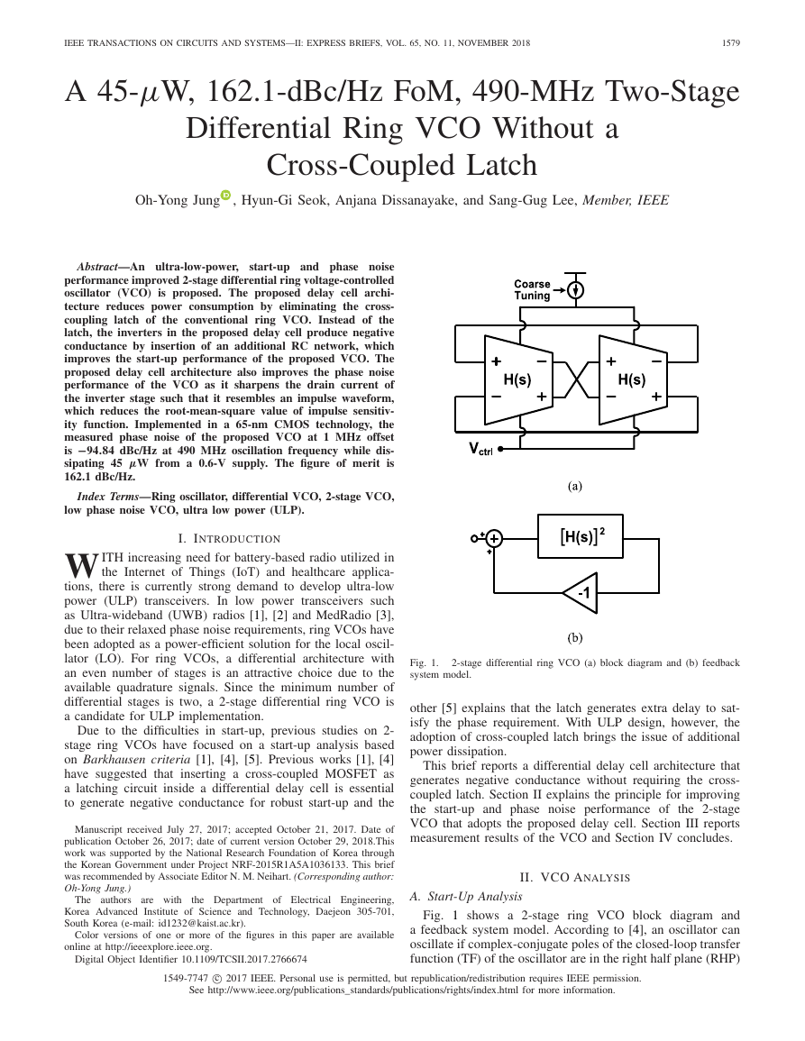
Fig. 1.
system model.
2-stage differential ring VCO (a) block diagram and (b) feedback
other [5] explains that the latch generates extra delay to sat-
isfy the phase requirement. With ULP design, however, the
adoption of cross-coupled latch brings the issue of additional
power dissipation.
This brief reports a differential delay cell architecture that
generates negative conductance without requiring the cross-
coupled latch. Section II explains the principle for improving
the start-up and phase noise performance of the 2-stage
VCO that adopts the proposed delay cell. Section III reports
measurement results of the VCO and Section IV concludes.
II. VCO ANALYSIS
A. Start-Up Analysis
Fig. 1 shows a 2-stage ring VCO block diagram and
a feedback system model. According to [4], an oscillator can
oscillate if complex-conjugate poles of the closed-loop transfer
function (TF) of the oscillator are in the right half plane (RHP)
�
1580
IEEE TRANSACTIONS ON CIRCUITS AND SYSTEMS—II: EXPRESS BRIEFS, VOL. 65, NO. 11, NOVEMBER 2018
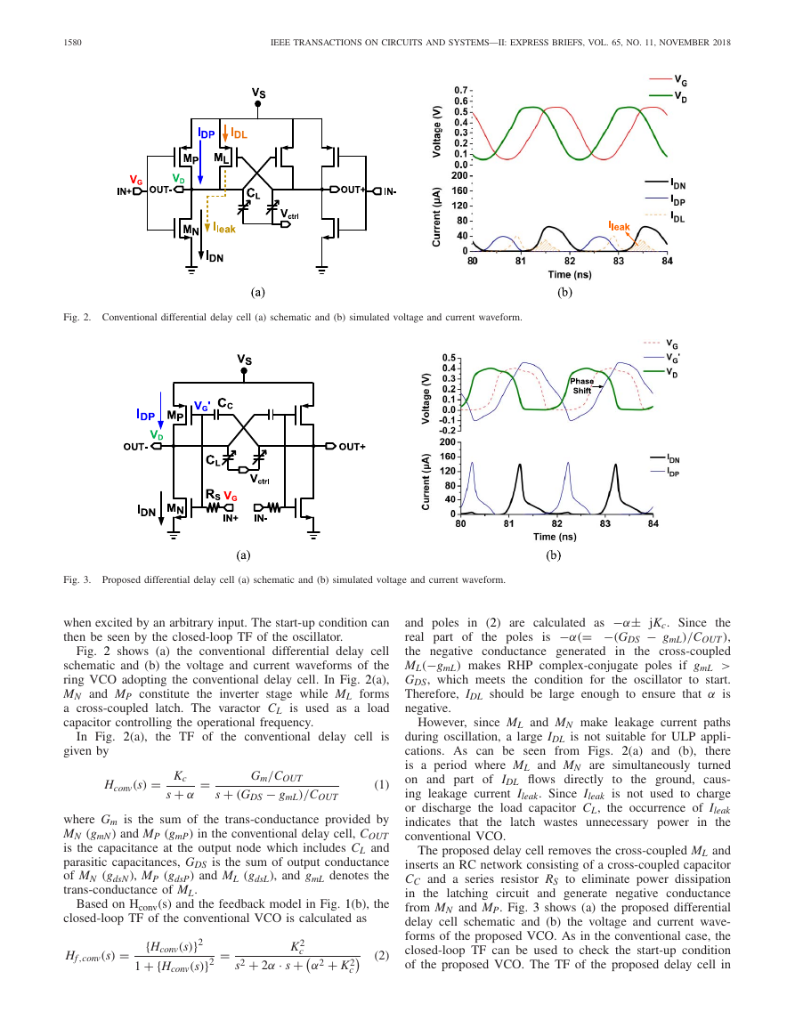
Fig. 2. Conventional differential delay cell (a) schematic and (b) simulated voltage and current waveform.
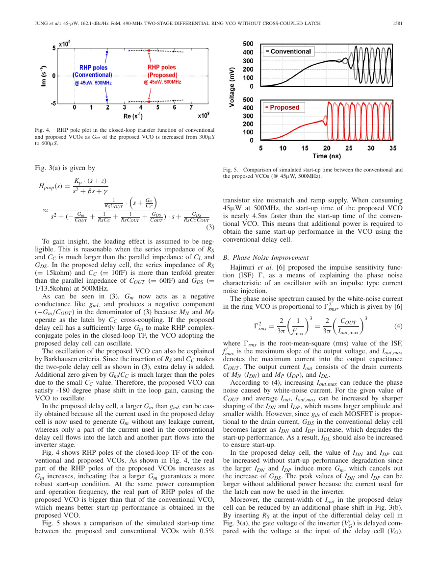
Fig. 3. Proposed differential delay cell (a) schematic and (b) simulated voltage and current waveform.
when excited by an arbitrary input. The start-up condition can
then be seen by the closed-loop TF of the oscillator.
Fig. 2 shows (a) the conventional differential delay cell
schematic and (b) the voltage and current waveforms of the
ring VCO adopting the conventional delay cell. In Fig. 2(a),
MN and MP constitute the inverter stage while ML forms
a cross-coupled latch. The varactor CL is used as a load
capacitor controlling the operational frequency.
is
In Fig. 2(a),
the TF of the conventional delay cell
given by
Hconv(s) = Kc
s + α
=
Gm/COUT
s + (GDS − gmL)/COUT
(1)
where Gm is the sum of the trans-conductance provided by
MN (gmN) and MP (gmP) in the conventional delay cell, COUT
is the capacitance at the output node which includes CL and
parasitic capacitances, GDS is the sum of output conductance
of MN (gdsN), MP (gdsP) and ML (gdsL), and gmL denotes the
trans-conductance of ML.
Based on Hconv(s) and the feedback model in Fig. 1(b), the
closed-loop TF of the conventional VCO is calculated as
Hf ,conv(s) = {Hconv(s)}2
1 + {Hconv(s)}2
=
K2
s2 + 2α · s +
c
α2 + K2
c
(2)
and poles in (2) are calculated as −α± jKc. Since the
the poles is −α(= −(GDS − gmL)/COUT ),
real part of
the negative conductance generated in the cross-coupled
ML(−gmL) makes RHP complex-conjugate poles if gmL >
GDS, which meets the condition for the oscillator to start.
Therefore, IDL should be large enough to ensure that α is
negative.
However, since ML and MN make leakage current paths
during oscillation, a large IDL is not suitable for ULP appli-
cations. As can be seen from Figs. 2(a) and (b),
there
is a period where ML and MN are simultaneously turned
on and part of IDL flows directly to the ground, caus-
ing leakage current Ileak. Since Ileak is not used to charge
or discharge the load capacitor CL, the occurrence of Ileak
indicates that
the latch wastes unnecessary power in the
conventional VCO.
The proposed delay cell removes the cross-coupled ML and
inserts an RC network consisting of a cross-coupled capacitor
CC and a series resistor RS to eliminate power dissipation
in the latching circuit and generate negative conductance
from MN and MP. Fig. 3 shows (a) the proposed differential
delay cell schematic and (b) the voltage and current wave-
forms of the proposed VCO. As in the conventional case, the
closed-loop TF can be used to check the start-up condition
of the proposed VCO. The TF of the proposed delay cell in
�
JUNG et al.: 45-μW, 162.1-dBc/Hz FoM, 490-MHz TWO-STAGE DIFFERENTIAL RING VCO WITHOUT CROSS-COUPLED LATCH
1581
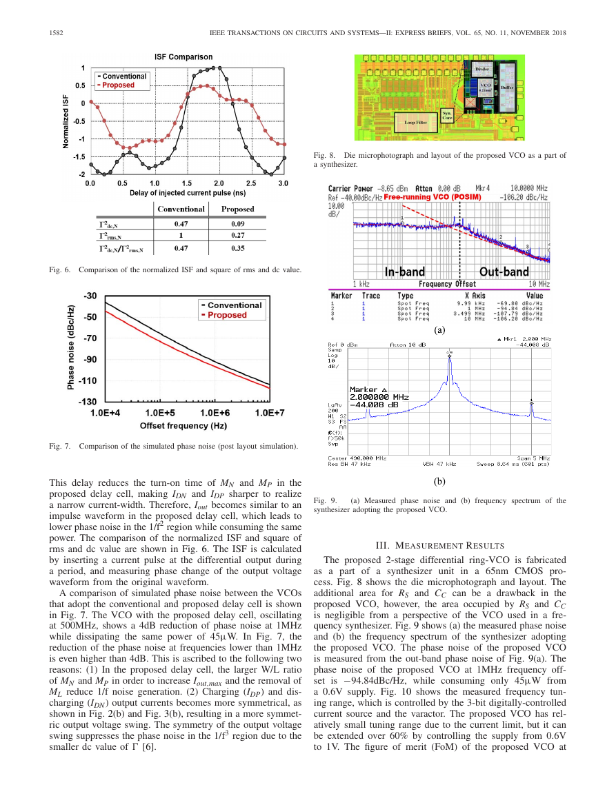
Fig. 4. RHP pole plot in the closed-loop transfer function of conventional
and proposed VCOs as Gm of the proposed VCO is increased from 300µS
to 600µS.
Fig. 3(a) is given by
Hprop(s) = Kp · (s + z)
s2 + βs + γ
≈
s2 + (− Gm
+ 1
RSCC
COUT
RSCOUT
1
·
s + Gm
+ 1
RSCOUT
CC
+ GDS
COUT
) · s + GDS
RSCCCOUT
(3)
To gain insight, the loading effect is assumed to be neg-
ligible. This is reasonable when the series impedance of RS
and CC is much larger than the parallel impedance of CL and
GDS. In the proposed delay cell, the series impedance of RS
(= 15kohm) and CC (= 10fF) is more than tenfold greater
than the parallel impedance of COUT (= 60fF) and GDS (=
1/13.5kohm) at 500MHz.
As can be seen in (3), Gm now acts as a negative
conductance like gmL and produces a negative component
(−Gm/COUT) in the denominator of (3) because MN and MP
operate as the latch by CC cross-coupling. If the proposed
delay cell has a sufficiently large Gm to make RHP complex-
conjugate poles in the closed-loop TF, the VCO adopting the
proposed delay cell can oscillate.
The oscillation of the proposed VCO can also be explained
by Barkhausen criteria. Since the insertion of RS and CC makes
the two-pole delay cell as shown in (3), extra delay is added.
Additional zero given by Gm/CC is much larger than the poles
due to the small CC value. Therefore, the proposed VCO can
satisfy -180 degree phase shift in the loop gain, causing the
VCO to oscillate.
In the proposed delay cell, a larger Gm than gmL can be eas-
ily obtained because all the current used in the proposed delay
cell is now used to generate Gm without any leakage current,
whereas only a part of the current used in the conventional
delay cell flows into the latch and another part flows into the
inverter stage.
Fig. 4 shows RHP poles of the closed-loop TF of the con-
ventional and proposed VCOs. As shown in Fig. 4, the real
part of the RHP poles of the proposed VCOs increases as
Gm increases, indicating that a larger Gm guarantees a more
robust start-up condition. At the same power consumption
and operation frequency, the real part of RHP poles of the
proposed VCO is bigger than that of the conventional VCO,
which means better start-up performance is obtained in the
proposed VCO.
Fig. 5 shows a comparison of the simulated start-up time
between the proposed and conventional VCOs with 0.5%
Fig. 5. Comparison of simulated start-up time between the conventional and
the proposed VCOs (@ 45µW, 500MHz).
transistor size mismatch and ramp supply. When consuming
45µW at 500MHz, the start-up time of the proposed VCO
is nearly 4.5ns faster than the start-up time of the conven-
tional VCO. This means that additional power is required to
obtain the same start-up performance in the VCO using the
conventional delay cell.
B. Phase Noise Improvement
Hajimiri et al. [6] proposed the impulse sensitivity func-
tion (ISF) �, as a means of explaining the phase noise
characteristic of an oscillator with an impulse type current
noise injection.
in the ring VCO is proportional to �2
The phase noise spectrum caused by the white-noise current
rms, which is given by [6]
(4)
�2
rms
= 2
3π
3 = 2
3π
1
f
max
3
COUT
Iout,max
where �rms is the root-mean-square (rms) value of the ISF,
max is the maximum slope of the output voltage, and Iout,max
f
denotes the maximum current
into the output capacitance
COUT. The output current Iout consists of the drain currents
of MN (IDN) and MP (IDP), and IDL.
According to (4), increasing Iout,max can reduce the phase
noise caused by white-noise current. For the given value of
COUT and average Iout, Iout,max can be increased by sharper
shaping of the IDN and IDP, which means larger amplitude and
smaller width. However, since gds of each MOSFET is propor-
tional to the drain current, GDS in the conventional delay cell
becomes larger as IDN and IDP increase, which degrades the
start-up performance. As a result, IDL should also be increased
to ensure start-up.
In the proposed delay cell, the value of IDN and IDP can
be increased without start-up performance degradation since
the larger IDN and IDP induce more Gm, which cancels out
the increase of GDS. The peak values of IDN and IDP can be
larger without additional power because the current used for
the latch can now be used in the inverter.
Moreover, the current-width of Iout in the proposed delay
cell can be reduced by an additional phase shift in Fig. 3(b).
By inserting RS at the input of the differential delay cell in
Fig. 3(a), the gate voltage of the inverter (V
G) is delayed com-
pared with the voltage at the input of the delay cell (VG).
�
1582
IEEE TRANSACTIONS ON CIRCUITS AND SYSTEMS—II: EXPRESS BRIEFS, VOL. 65, NO. 11, NOVEMBER 2018
Fig. 8. Die microphotograph and layout of the proposed VCO as a part of
a synthesizer.
Fig. 6. Comparison of the normalized ISF and square of rms and dc value.
Fig. 7. Comparison of the simulated phase noise (post layout simulation).
This delay reduces the turn-on time of MN and MP in the
proposed delay cell, making IDN and IDP sharper to realize
a narrow current-width. Therefore, Iout becomes similar to an
impulse waveform in the proposed delay cell, which leads to
lower phase noise in the 1/f2 region while consuming the same
power. The comparison of the normalized ISF and square of
rms and dc value are shown in Fig. 6. The ISF is calculated
by inserting a current pulse at the differential output during
a period, and measuring phase change of the output voltage
waveform from the original waveform.
A comparison of simulated phase noise between the VCOs
that adopt the conventional and proposed delay cell is shown
in Fig. 7. The VCO with the proposed delay cell, oscillating
at 500MHz, shows a 4dB reduction of phase noise at 1MHz
while dissipating the same power of 45µW. In Fig. 7, the
reduction of the phase noise at frequencies lower than 1MHz
is even higher than 4dB. This is ascribed to the following two
reasons: (1) In the proposed delay cell, the larger W/L ratio
of MN and MP in order to increase Iout,max and the removal of
ML reduce 1/f noise generation. (2) Charging (IDP) and dis-
charging (IDN) output currents becomes more symmetrical, as
shown in Fig. 2(b) and Fig. 3(b), resulting in a more symmet-
ric output voltage swing. The symmetry of the output voltage
swing suppresses the phase noise in the 1/f3 region due to the
smaller dc value of � [6].
Fig. 9.
synthesizer adopting the proposed VCO.
(a) Measured phase noise and (b) frequency spectrum of the
III. MEASUREMENT RESULTS
The proposed 2-stage differential ring-VCO is fabricated
as a part of a synthesizer unit
in a 65nm CMOS pro-
cess. Fig. 8 shows the die microphotograph and layout. The
additional area for RS and CC can be a drawback in the
proposed VCO, however, the area occupied by RS and CC
is negligible from a perspective of the VCO used in a fre-
quency synthesizer. Fig. 9 shows (a) the measured phase noise
and (b) the frequency spectrum of the synthesizer adopting
the proposed VCO. The phase noise of the proposed VCO
is measured from the out-band phase noise of Fig. 9(a). The
phase noise of the proposed VCO at 1MHz frequency off-
is −94.84dBc/Hz, while consuming only 45µW from
set
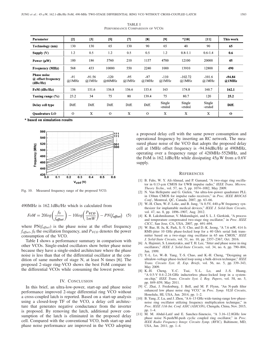
a 0.6V supply. Fig. 10 shows the measured frequency tun-
ing range, which is controlled by the 3-bit digitally-controlled
current source and the varactor. The proposed VCO has rel-
atively small tuning range due to the current limit, but it can
be extended over 60% by controlling the supply from 0.6V
to 1V. The figure of merit (FoM) of the proposed VCO at
�
JUNG et al.: 45-μW, 162.1-dBc/Hz FoM, 490-MHz TWO-STAGE DIFFERENTIAL RING VCO WITHOUT CROSS-COUPLED LATCH
1583
TABLE I
PERFORMANCE COMPARISON OF VCOS
a proposed delay cell with the same power consumption and
operational frequency by inserting an RC network. The mea-
sured phase noise of the VCO that adopts the proposed delay
cell at 1MHz offset frequency is -94.84dBc/Hz at 490MHz,
operating over a frequency range of 428MHz-552MHz, and
the FoM is 162.1dBc/Hz while dissipating 45µW from a 0.6V
supply.
REFERENCES
[1] B. Fahs, W. Y. Ali-Ahmad, and P. Gamand, “A two-stage ring oscilla-
tor in 0.13-µm CMOS for UWB impulse radio,” IEEE Trans. Microw.
Theory Techn., vol. 57, no. 5, pp. 1074–1082, May 2009.
[2] N. Van Helleputte and G. Gielen, “An ultra-low-power quadrature PLL
in 130nm CMOS for impulse radio receivers,” in Proc. IEEE BIOCAS
Conf., Montreal, QC, Canada, 2007, pp. 63–66.
[3] W.-H. Chen, W.-F. Loke, and B. Jung, “A 0.5V, 440-µW frequency syn-
thesizer for implantable medical devices,” IEEE J. Solid-State Circuits,
vol. 47, no. 8, pp. 1896–1907, Aug. 2012.
[4] K. R. Lakshmikumar, V. Mukundagiri, and S. L. J. Gierkink, “A process
and temperature compensated two-stage ring oscillator,” in Proc. IEEE
CICC, San Jose, CA, USA, 2007, pp. 691–694.
[5] W. Bae, H. Ju, K. Park, S.-Y. Cho, and D.-K. Jeong, “A 7.6 mW, 414 fs
RMS-jitter 10 GHz phase-locked loop for a 40 Gb/s serial link trans-
mitter based on a two-stage ring oscillator in 65 nm CMOS,” IEEE
J. Solid-State Circuits, vol. 51, no. 10, pp. 2357–2367, Oct. 2016.
[6] A. Hajimiri, S. Limotyrakis, and T. H. Lee, “Jitter and phase noise in ring
oscillators,” IEEE J. Solid-State Circuits, vol. 34, no. 6, pp. 790–804,
Jun. 1999.
[7] Y.-L. Lo, W.-B. Yang, T.-S. Chao, and K.-H. Cheng, “Designing an
ultralow-voltage phase-locked loop using a bulk-driven technique,” IEEE
Trans. Circuits Syst. II, Exp. Briefs, vol. 56, no. 5, pp. 339–343,
May 2009.
[8] K.-H. Cheng, Y.-C.
J.-S. Huang,
“A 0.5-V 0.4–2.24-GHz inductorless phase-locked loop in a system-
on-chip,” IEEE Trans. Circuits Syst. I, Reg. Papers, vol. 58, no. 5,
pp. 849–859, May 2011.
Tsai, Y.-L.
and
Lo,
Fig. 10. Measured frequency range of the proposed VCO.
490MHz is 162.1dBc/Hz which is calculated from
− PN
foffset
FoM = 20log
− 10log
(5)
f0
foffset
PVCO
1mW
where PN(foffset) is the phase noise at the offset frequency
foffset, f0 the oscillation frequency, and PVCO denotes the power
consumption of the VCO.
Table I shows a performance summary in comparison with
other VCOs. Single-ended oscillators show better phase noise
because they have a single-ended architecture where the phase
noise is less than that of the differential oscillator at the con-
dition of same number of stage N, at least N times [6]. The
proposed 2-stage ring-VCO shows the best FoM compare to
the differential VCOs while consuming the lowest power.
IV. CONCLUSION
In this brief, an ultra-low-power, start-up and phase noise
performance improved 2-stage differential ring VCO without
a cross-coupled latch is reported. Based on a start-up analysis
using a closed-loop TF of the VCO, a delay cell architec-
ture that generates negative conductance from the inverter
is proposed. By removing the latch, additional power con-
sumption of the latch is eliminated in the proposed delay
cell. Compared with the conventional VCO, both start-up and
phase noise performance are improved in the VCO adopting
[9] C. Zhai, J. Fredenburg, J. Bell, and M. P. Flynn, “An N-path filter
enhanced low phase noise ring VCO,” in Proc. Symp. VLSI Circuits,
Honolulu, HI, USA, Jun. 2014, pp. 1–2.
[10] B. Yang, Z. Lu, and J. Zhou, “A 6–13 GHz wide-tuning-range low-phase-
noise ring oscillator utilizing frequency multiplication technique,” in
Proc. IEEE 11th Int. Conf. ASIC (ASICON), Chengdu, China, Nov. 2015,
pp. 1–4.
[11] M. M. Abdul-Latif and E. Sanchez-Sinencio, “A 3.16–12.8GHz low
phase noise N-push/M-push cyclic coupled ring oscillator,” in Proc.
IEEE Radio Frequency Integr. Circuits Symp. (RFIC), Baltimore, MD,
USA, Jun. 2011, pp. 1–4.
�


 2023年江西萍乡中考道德与法治真题及答案.doc
 2012年重庆南川中考生物真题及答案.doc
 2013年江西师范大学地理学综合及文艺理论基础考研真题.doc
 2020年四川甘孜小升初语文真题及答案I卷.doc
 2020年注册岩土工程师专业基础考试真题及答案.doc
 2023-2024学年福建省厦门市九年级上学期数学月考试题及答案.doc
 2021-2022学年辽宁省沈阳市大东区九年级上学期语文期末试题及答案.doc
 2022-2023学年北京东城区初三第一学期物理期末试卷及答案.doc
 2018上半年江西教师资格初中地理学科知识与教学能力真题及答案.doc
 2012年河北国家公务员申论考试真题及答案-省级.doc
 2020-2021学年江苏省扬州市江都区邵樊片九年级上学期数学第一次质量检测试题及答案.doc
 2022下半年黑龙江教师资格证中学综合素质真题及答案.doc