D Available in the Texas Instruments
NanoStar and NanoFree Packages
D Supports 5-V VCC Operation
D Inputs Accept Voltages to 5.5 V
D Max tpd of 3.8 ns at 3.3 V
D Low Power Consumption, 10-µA Max ICC
D ±24-mA Output Drive at 3.3 V
SN74LVC1G00
SINGLE 2ĆINPUT POSITIVEĆNAND GATE
SCES212T − APRIL 1999 − REVISED JUNE 2005
D Ioff Supports Partial-Power-Down Mode
Operation
D Latch-Up Performance Exceeds 100 mA Per
JESD 78, Class II
D ESD Protection Exceeds JESD 22
− 2000-V Human-Body Model (A114-A)
− 200-V Machine Model (A115-A)
− 1000-V Charged-Device Model (C101)
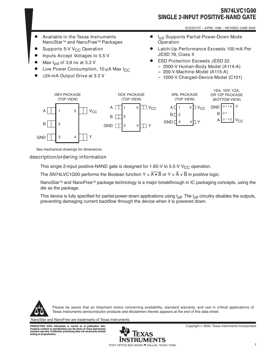
DBV PACKAGE
(TOP VIEW)
DCK PACKAGE
(TOP VIEW)
DRL PACKAGE
(TOP VIEW)
A
B
GND
1
2
3
5
4
VCC
Y
A
B
GND
1
2
3
5
4
VCC
Y
A
B
GND
1
2
3
5
4
VCC
Y
YEA, YEP, YZA,
OR YZP PACKAGE
(BOTTOM VIEW)
GND
B
A
3
4
2
1
5
Y
VCC
See mechanical drawings for dimensions.
description/ordering information
This single 2-input positive-NAND gate is designed for 1.65-V to 5.5-V VCC operation.
The SN74LVC1G00 performs the Boolean function Y = A • B or Y = A + B in positive logic.
NanoStar and NanoFree package technology is a major breakthrough in IC packaging concepts, using the
die as the package.
This device is fully specified for partial-power-down applications using Ioff. The Ioff circuitry disables the outputs,
preventing damaging current backflow through the device when it is powered down.
Please be aware that an important notice concerning availability, standard warranty, and use in critical applications of
Texas Instruments semiconductor products and disclaimers thereto appears at the end of this data sheet.
NanoStar and NanoFree are trademarks of Texas Instruments.
information
PRODUCTION DATA
is current as of publication date.
Products conform to specifications per the terms of Texas Instruments
standard warranty. Production processing does not necessarily include
testing of all parameters.
Copyright 2005, Texas Instruments Incorporated
POST OFFICE BOX 655303 • DALLAS, TEXAS 75265
1
�
SN74LVC1G00
SINGLE 2ĆINPUT POSITIVEĆNAND GATE
SCES212T − APRIL 1999 − REVISED JUNE 2005
TA
−40°C to 85°C
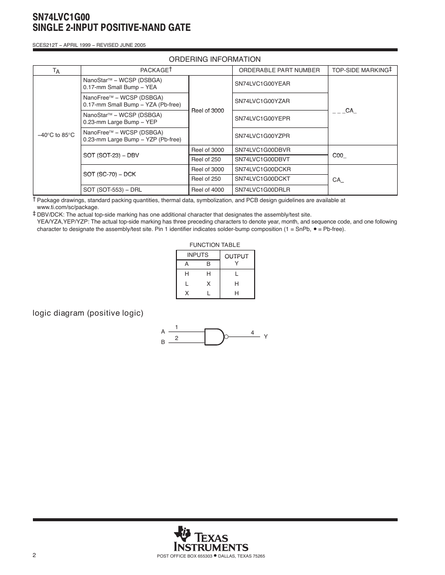
ORDERING INFORMATION
PACKAGE†
ORDERABLE PART NUMBER
TOP-SIDE MARKING‡
NanoStar − WCSP (DSBGA)
0.17-mm Small Bump − YEA
NanoFree − WCSP (DSBGA)
0.17-mm Small Bump − YZA (Pb-free)
NanoStar − WCSP (DSBGA)
0.23-mm Large Bump − YEP
NanoFree − WCSP (DSBGA)
0.23-mm Large Bump − YZP (Pb-free)
SOT (SOT-23) − DBV
SOT (SOT-23) − DBV
SOT (SC-70) − DCK
SOT (SC-70) − DCK
Reel of 3000
Reel of 3000
SN74LVC1G00YEAR
SN74LVC1G00YZAR
SN74LVC1G00YEPR
SN74LVC1G00YZPR
Reel of 3000
Reel of 250
Reel of 3000
Reel of 250
SN74LVC1G00DBVR
SN74LVC1G00DBVT
SN74LVC1G00DCKR
SN74LVC1G00DCKT
_ _ _CA_
_ _ _CA_
C00_
C00_
CA_
CA_
SOT (SOT-553) − DRL
Reel of 4000
SN74LVC1G00DRLR
† Package drawings, standard packing quantities, thermal data, symbolization, and PCB design guidelines are available at
www.ti.com/sc/package.
‡ DBV/DCK: The actual top-side marking has one additional character that designates the assembly/test site.
YEA/YZA,YEP/YZP: The actual top-side marking has three preceding characters to denote year, month, and sequence code, and one following
character to designate the assembly/test site. Pin 1 identifier indicates solder-bump composition (1 = SnPb, • = Pb-free).
OUTPUT
OUTPUT
Y
FUNCTION TABLE
INPUTS
B
A
H
H
X
L
X
L
L
H
H
logic diagram (positive logic)
1
2
A
B
4
Y
2
POST OFFICE BOX 655303 • DALLAS, TEXAS 75265
�
SCES212T − APRIL 1999 − REVISED JUNE 2005
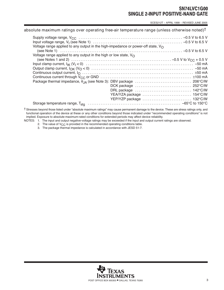
absolute maximum ratings over operating free-air temperature range (unless otherwise noted)†
SN74LVC1G00
SINGLE 2ĆINPUT POSITIVEĆNAND GATE
Supply voltage range, VCC
Input voltage range, VI (see Note 1)
Voltage range applied to any output in the high-impedance or power-off state, VO
. . . . . . . . . . . . . . . . . . . . . . . . . . . . . . . . . . . . . . . . . . . . . . . . . . . . . . . . .
. . . . . . . . . . . . . . . . . . . . . . . . . . . . . . . . . . . . . . . . . . . . . . . . .
(see Note 1)
. . . . . . . . . . . . . . . . . . . . . . . . . . . . . . . . . . . . . . . . . . . . . . . . . . . . . . . . . . . . . . . . . . .
−0.5 V to 6.5 V
−0.5 V to 6.5 V
−0.5 V to 6.5 V
Voltage range applied to any output in the high or low state, VO
(see Notes 1 and 2)
. . . . . . . . . . . . . . . . . . . . . . . . . . . . . . . . . . . . . . . . . . . . . . . . . . . . . . .
Input clamp current, IIK (VI < 0)
Output clamp current, IOK (VO < 0)
Continuous output current, IO
Continuous current through VCC or GND
Package thermal impedance, θJA (see Note 3): DBV package
DCK package
DRL package
YEA/YZA package
YEP/YZP package
−0.5 V to VCC + 0.5 V
−50 mA
−50 mA
±50 mA
±100 mA
206°C/W
252°C/W
142°C/W
154°C/W
132°C/W
−65°C to 150°C
† Stresses beyond those listed under “absolute maximum ratings” may cause permanent damage to the device. These are stress ratings only, and
functional operation of the device at these or any other conditions beyond those indicated under “recommended operating conditions” is not
implied. Exposure to absolute-maximum-rated conditions for extended periods may affect device reliability.
. . . . . . . . . . . . . . . . . . . . . . . . . . . . . . . . . . . . . . . . . . . . . . . . . . . . . . . . . . .
. . . . . . . . . . . . . . . . . . . . . . . . . . . . . . . . . . . . . . . . . . . . . . . . . . . . . . . .
. . . . . . . . . . . . . . . . . . . . . . . . . . . . . . . . . . . . . . . . . . . . . . . . . . . . . . . . . . . . .
. . . . . . . . . . . . . . . . . . . . . . . . . . . . . . . . . . . . . . . . . . . . . . . . . .
. . . . . . . . . . . . . . . . . . . . . . . . . . . . . . .
. . . . . . . . . . . . . . . . . . . . . . . . . . . . . . .
. . . . . . . . . . . . . . . . . . . . . . . . . . . . . . .
. . . . . . . . . . . . . . . . . . . . . . . . . . .
. . . . . . . . . . . . . . . . . . . . . . . . . . .
. . . . . . . . . . . . . . . . . . . . . . . . . . . . . . . . . . . . . . . . . . . . . . . . . . .
Storage temperature range, Tstg
NOTES: 1. The input and output negative-voltage ratings may be exceeded if the input and output current ratings are observed.
2. The value of VCC is provided in the recommended operating conditions table.
3. The package thermal impedance is calculated in accordance with JESD 51-7.
POST OFFICE BOX 655303 • DALLAS, TEXAS 75265
3
�
SN74LVC1G00
SINGLE 2ĆINPUT POSITIVEĆNAND GATE
SCES212T − APRIL 1999 − REVISED JUNE 2005
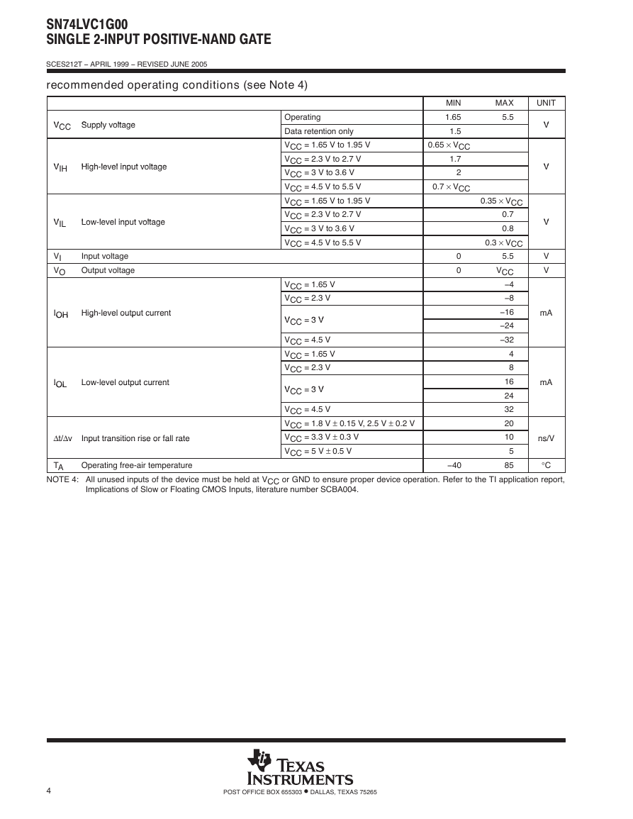
recommended operating conditions (see Note 4)
VCC Supply voltage
VCC Supply voltage
VIH
VIH
High-level input voltage
High-level input voltage
VIL
VIL
VI
VO
Low-level input voltage
Low-level input voltage
Input voltage
Output voltage
IOH
IOH
High-level output current
High-level output current
IOL
IOL
Low-level output current
Low-level output current
∆t/∆v
∆t/∆v
TA
Input transition rise or fall rate
Input transition rise or fall rate
Operating free-air temperature
Operating
Data retention only
VCC = 1.65 V to 1.95 V
VCC = 2.3 V to 2.7 V
VCC = 3 V to 3.6 V
VCC = 4.5 V to 5.5 V
VCC = 1.65 V to 1.95 V
VCC = 2.3 V to 2.7 V
VCC = 3 V to 3.6 V
VCC = 4.5 V to 5.5 V
VCC = 1.65 V
VCC = 2.3 V
VCC = 3 V
VCC = 3 V
VCC = 4.5 V
VCC = 1.65 V
VCC = 2.3 V
VCC = 3 V
VCC = 3 V
VCC = 4.5 V
VCC = 1.8 V ± 0.15 V, 2.5 V ± 0.2 V
VCC = 3.3 V ± 0.3 V
VCC = 5 V ± 0.5 V
MIN
1.65
1.5
0.65 × VCC
1.7
2
0.7 × VCC
MAX
5.5
0.35 × VCC
0.7
0.8
0.3 × VCC
0
0
−40
5.5
VCC
−4
−8
−16
−24
−32
4
8
16
24
32
20
10
5
85
UNIT
V
V
V
V
V
V
V
V
mA
mA
mA
mA
ns/V
ns/V
°C
NOTE 4: All unused inputs of the device must be held at VCC or GND to ensure proper device operation. Refer to the TI application report,
Implications of Slow or Floating CMOS Inputs, literature number SCBA004.
4
POST OFFICE BOX 655303 • DALLAS, TEXAS 75265
�
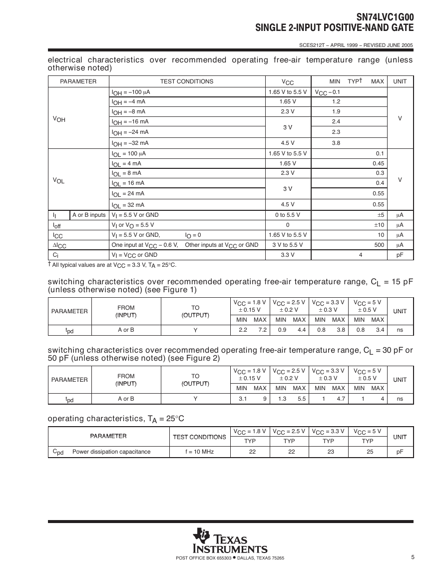
electrical characteristics over recommended operating free-air temperature range (unless
otherwise noted)
SN74LVC1G00
SINGLE 2ĆINPUT POSITIVEĆNAND GATE
SCES212T − APRIL 1999 − REVISED JUNE 2005
PARAMETER
TEST CONDITIONS
V
VOH
V
VOL
IOH = −100 mA
IOH = −4 mA
IOH = −8 mA
IOH = −16 mA
IOH = −24 mA
IOH = −32 mA
IOL = 100 mA
IOL = 4 mA
IOL = 8 mA
IOL = 16 mA
IOL = 24 mA
IOL = 32 mA
A or B inputs VI = 5.5 V or GND
II
Ioff
ICC
∆ICC
Ci
† All typical values are at VCC = 3.3 V, TA = 25°C.
VI or VO = 5.5 V
VI = 5.5 V or GND,
One input at VCC − 0.6 V, Other inputs at VCC or GND
VI = VCC or GND
IO = 0
VCC
1.65 V to 5.5 V
1.65 V
2.3 V
3 V
3 V
4.5 V
1.65 V to 5.5 V
1.65 V
2.3 V
3 V
3 V
4.5 V
0 to 5.5 V
0
1.65 V to 5.5 V
3 V to 5.5 V
3.3 V
MIN TYP† MAX
UNIT
VCC − 0.1
1.2
1.9
2.4
2.3
3.8
V
V
V
V
mA
mA
mA
mA
pF
0.1
0.45
0.3
0.4
0.55
0.55
±5
±10
10
500
4
switching characteristics over recommended operating free-air temperature range, CL = 15 pF
(unless otherwise noted) (see Figure 1)
PARAMETER
PARAMETER
tpd
FROM
(INPUT)
(INPUT)
A or B
TO
(OUTPUT)
(OUTPUT)
Y
VCC = 1.8 V
VCC = 2.5 V
VCC = 3.3 V
± 0.2 V
± 0.15 V
MIN MAX MIN MAX MIN MAX MIN MAX
3.4
2.2
± 0.3 V
± 0.5 V
7.2
0.9
4.4
0.8
3.8
0.8
VCC = 5 V
UNIT
UNIT
ns
switching characteristics over recommended operating free-air temperature range, CL = 30 pF or
50 pF (unless otherwise noted) (see Figure 2)
PARAMETER
PARAMETER
tpd
FROM
(INPUT)
(INPUT)
A or B
TO
(OUTPUT)
(OUTPUT)
Y
operating characteristics, TA = 25°C
VCC = 1.8 V
VCC = 2.5 V
VCC = 3.3 V
± 0.2 V
± 0.15 V
MIN MAX MIN MAX MIN MAX MIN MAX
4
3.1
± 0.3 V
± 0.5 V
1.3
5.5
4.7
9
1
1
VCC = 5 V
PARAMETER
PARAMETER
TEST CONDITIONS
TEST CONDITIONS
Cpd
Power dissipation capacitance
f = 10 MHz
VCC = 1.8 V VCC = 2.5 V VCC = 3.3 V
VCC = 5 V
TYP
22
TYP
22
TYP
23
TYP
25
UNIT
UNIT
ns
UNIT
UNIT
pF
POST OFFICE BOX 655303 • DALLAS, TEXAS 75265
5
�
SN74LVC1G00
SINGLE 2ĆINPUT POSITIVEĆNAND GATE
SCES212T − APRIL 1999 − REVISED JUNE 2005
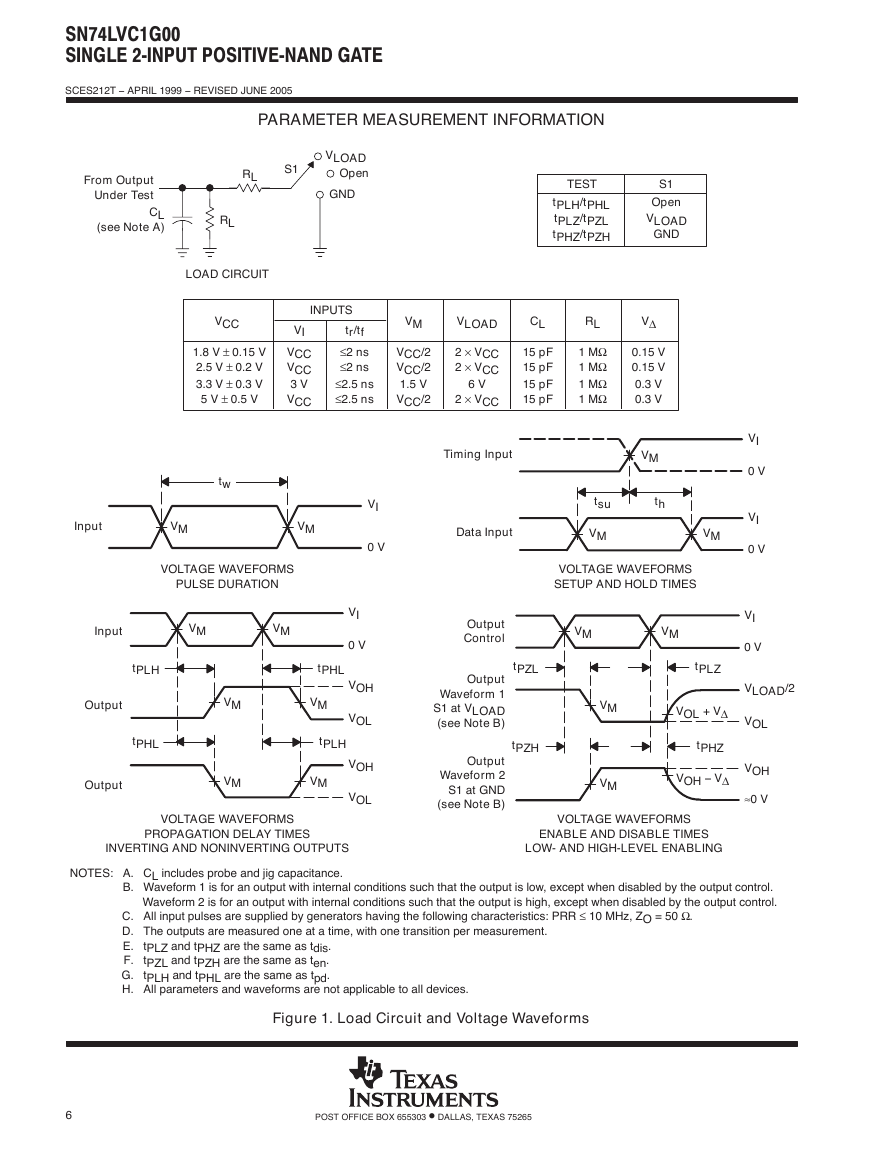
PARAMETER MEASUREMENT INFORMATION
S1
RL
VLOAD
Open
GND
From Output
Under Test
CL
(see Note A)
RL
TEST
tPLH/tPHL
tPLZ/tPZL
tPHZ/tPZH
S1
Open
VLOAD
GND
LOAD CIRCUIT
VCC
1.8 V ± 0.15 V
2.5 V ± 0.2 V
3.3 V ± 0.3 V
5 V ± 0.5 V
INPUTS
VI
VCC
VCC
3 V
VCC
tr/tf
≤2 ns
≤2 ns
≤2.5 ns
≤2.5 ns
VM
VCC/2
VCC/2
1.5 V
VCC/2
VLOAD
2 × VCC
2 × VCC
6 V
2 × VCC
CL
15 pF
15 pF
15 pF
15 pF
RL
1 MΩ
1 MΩ
1 MΩ
1 MΩ
tw
Input
VM
VM
Timing Input
Data Input
VI
0 V
tsu
VM
V∆
0.15 V
0.15 V
0.3 V
0.3 V
VM
th
VOLTAGE WAVEFORMS
PULSE DURATION
Input
VM
VM
tPLH
tPHL
Output
Output
VM
VM
VI
0 V
VOH
VOL
VOH
VOL
tPHL
VM
tPLH
VM
Output
Control
Output
Waveform 1
S1 at VLOAD
(see Note B)
Output
Waveform 2
S1 at GND
(see Note B)
tPZL
tPZH
VM
VI
0 V
VI
0 V
VI
0 V
VOLTAGE WAVEFORMS
SETUP AND HOLD TIMES
VM
VM
tPLZ
VOL + V∆
tPHZ
VOH − V∆
VLOAD/2
VOL
VOH
≈0 V
VM
VM
VOLTAGE WAVEFORMS
PROPAGATION DELAY TIMES
INVERTING AND NONINVERTING OUTPUTS
VOLTAGE WAVEFORMS
ENABLE AND DISABLE TIMES
LOW- AND HIGH-LEVEL ENABLING
NOTES: A. CL includes probe and jig capacitance.
B. Waveform 1 is for an output with internal conditions such that the output is low, except when disabled by the output control.
Waveform 2 is for an output with internal conditions such that the output is high, except when disabled by the output control.
C. All input pulses are supplied by generators having the following characteristics: PRR ≤ 10 MHz, ZO = 50 Ω.
D. The outputs are measured one at a time, with one transition per measurement.
E.
F.
G.
H. All parameters and waveforms are not applicable to all devices.
tPLZ and tPHZ are the same as tdis.
tPZL and tPZH are the same as ten.
tPLH and tPHL are the same as tpd.
Figure 1. Load Circuit and Voltage Waveforms
6
POST OFFICE BOX 655303 • DALLAS, TEXAS 75265
�
SN74LVC1G00
SINGLE 2ĆINPUT POSITIVEĆNAND GATE
SCES212T − APRIL 1999 − REVISED JUNE 2005
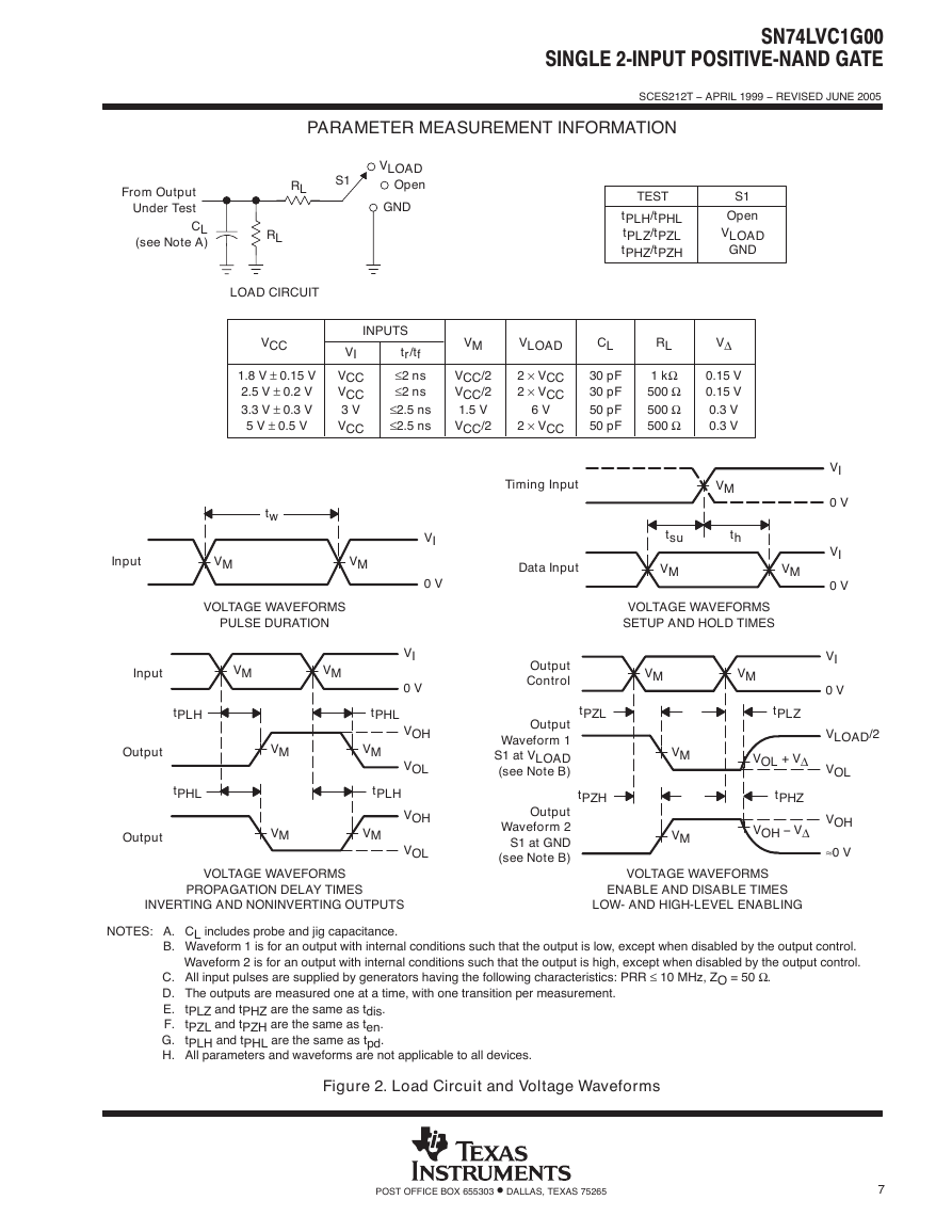
PARAMETER MEASUREMENT INFORMATION
S1
RL
VLOAD
Open
GND
From Output
Under Test
CL
(see Note A)
RL
TEST
tPLH/tPHL
tPLZ/tPZL
tPHZ/tPZH
S1
Open
VLOAD
GND
LOAD CIRCUIT
VCC
1.8 V ± 0.15 V
2.5 V ± 0.2 V
3.3 V ± 0.3 V
5 V ± 0.5 V
INPUTS
VI
VCC
VCC
3 V
VCC
tr/tf
≤2 ns
≤2 ns
≤2.5 ns
≤2.5 ns
VM
VCC/2
VCC/2
1.5 V
VCC/2
VLOAD
2 × VCC
2 × VCC
6 V
2 × VCC
CL
30 pF
30 pF
50 pF
50 pF
RL
1 kΩ
500 Ω
500 Ω
500 Ω
tw
Input
VM
VM
Timing Input
Data Input
VI
0 V
tsu
VM
V∆
0.15 V
0.15 V
0.3 V
0.3 V
VM
th
VOLTAGE WAVEFORMS
PULSE DURATION
Input
VM
VM
tPLH
tPHL
Output
Output
VM
VM
VI
0 V
VOH
VOL
VOH
VOL
tPHL
VM
tPLH
VM
Output
Control
Output
Waveform 1
S1 at VLOAD
(see Note B)
Output
Waveform 2
S1 at GND
(see Note B)
tPZL
tPZH
VM
VI
0 V
VI
0 V
VI
0 V
VOLTAGE WAVEFORMS
SETUP AND HOLD TIMES
VM
VM
tPLZ
VOL + V∆
tPHZ
VOH − V∆
VLOAD/2
VOL
VOH
≈0 V
VM
VM
VOLTAGE WAVEFORMS
PROPAGATION DELAY TIMES
INVERTING AND NONINVERTING OUTPUTS
VOLTAGE WAVEFORMS
ENABLE AND DISABLE TIMES
LOW- AND HIGH-LEVEL ENABLING
NOTES: A. CL includes probe and jig capacitance.
B. Waveform 1 is for an output with internal conditions such that the output is low, except when disabled by the output control.
Waveform 2 is for an output with internal conditions such that the output is high, except when disabled by the output control.
C. All input pulses are supplied by generators having the following characteristics: PRR ≤ 10 MHz, ZO = 50 Ω.
D. The outputs are measured one at a time, with one transition per measurement.
E.
F.
G.
H. All parameters and waveforms are not applicable to all devices.
tPLZ and tPHZ are the same as tdis.
tPZL and tPZH are the same as ten.
tPLH and tPHL are the same as tpd.
Figure 2. Load Circuit and Voltage Waveforms
POST OFFICE BOX 655303 • DALLAS, TEXAS 75265
7
�
www.ti.com
10-Oct-2005
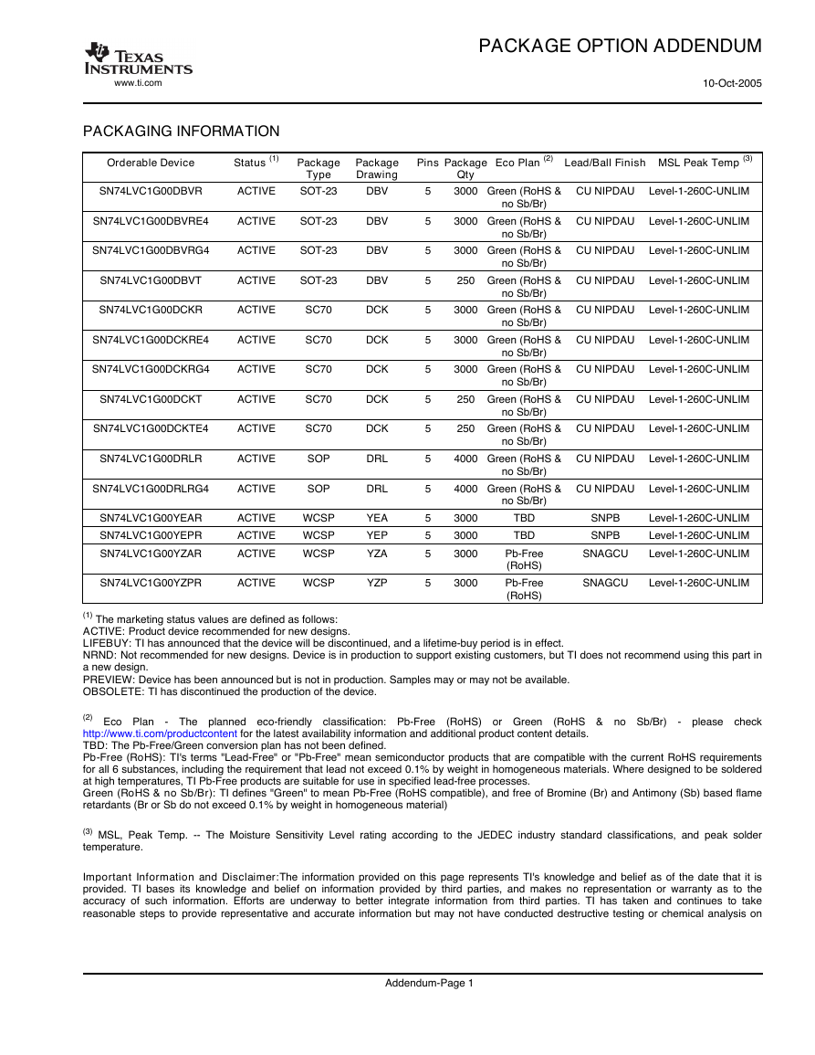
PACKAGE OPTION ADDENDUM
PACKAGING INFORMATION
Orderable Device
Status (1)
SN74LVC1G00DBVR
ACTIVE
Package
Type
SOT-23
Package
Drawing
DBV
SN74LVC1G00DBVRE4
ACTIVE
SOT-23
DBV
SN74LVC1G00DBVRG4
ACTIVE
SOT-23
DBV
SN74LVC1G00DBVT
ACTIVE
SOT-23
DBV
SN74LVC1G00DCKR
ACTIVE
SC70
SN74LVC1G00DCKRE4
ACTIVE
SC70
SN74LVC1G00DCKRG4
ACTIVE
SC70
SN74LVC1G00DCKT
ACTIVE
SC70
SN74LVC1G00DCKTE4
ACTIVE
SC70
SN74LVC1G00DRLR
ACTIVE
SN74LVC1G00DRLRG4
ACTIVE
SN74LVC1G00YEAR
SN74LVC1G00YEPR
SN74LVC1G00YZAR
ACTIVE
ACTIVE
ACTIVE
SOP
SOP
WCSP
WCSP
WCSP
SN74LVC1G00YZPR
ACTIVE
WCSP
DCK
DCK
DCK
DCK
DCK
DRL
DRL
YEA
YEP
YZA
YZP
Pins Package
Eco Plan (2) Lead/Ball Finish MSL Peak Temp (3)
Qty
3000 Green (RoHS &
5
5
5
5
5
5
5
5
5
5
5
5
5
5
5
CU NIPDAU Level-1-260C-UNLIM
no Sb/Br)
3000 Green (RoHS &
CU NIPDAU Level-1-260C-UNLIM
no Sb/Br)
3000 Green (RoHS &
CU NIPDAU Level-1-260C-UNLIM
no Sb/Br)
250 Green (RoHS &
CU NIPDAU Level-1-260C-UNLIM
no Sb/Br)
3000 Green (RoHS &
CU NIPDAU Level-1-260C-UNLIM
no Sb/Br)
3000 Green (RoHS &
CU NIPDAU Level-1-260C-UNLIM
no Sb/Br)
3000 Green (RoHS &
CU NIPDAU Level-1-260C-UNLIM
no Sb/Br)
250 Green (RoHS &
CU NIPDAU Level-1-260C-UNLIM
no Sb/Br)
250 Green (RoHS &
CU NIPDAU Level-1-260C-UNLIM
no Sb/Br)
4000 Green (RoHS &
CU NIPDAU Level-1-260C-UNLIM
no Sb/Br)
4000 Green (RoHS &
CU NIPDAU Level-1-260C-UNLIM
3000
3000
3000
3000
no Sb/Br)
TBD
TBD
Pb-Free
(RoHS)
Pb-Free
(RoHS)
SNPB
SNPB
SNAGCU
Level-1-260C-UNLIM
Level-1-260C-UNLIM
Level-1-260C-UNLIM
SNAGCU
Level-1-260C-UNLIM
(1) The marketing status values are defined as follows:
ACTIVE: Product device recommended for new designs.
LIFEBUY: TI has announced that the device will be discontinued, and a lifetime-buy period is in effect.
NRND: Not recommended for new designs. Device is in production to support existing customers, but TI does not recommend using this part in
a new design.
PREVIEW: Device has been announced but is not in production. Samples may or may not be available.
OBSOLETE: TI has discontinued the production of the device.
classification: Pb-Free (RoHS) or Green (RoHS & no Sb/Br)
(2) Eco Plan - The planned eco-friendly
http://www.ti.com/productcontent for the latest availability information and additional product content details.
TBD: The Pb-Free/Green conversion plan has not been defined.
Pb-Free (RoHS): TI's terms "Lead-Free" or "Pb-Free" mean semiconductor products that are compatible with the current RoHS requirements
for all 6 substances, including the requirement that lead not exceed 0.1% by weight in homogeneous materials. Where designed to be soldered
at high temperatures, TI Pb-Free products are suitable for use in specified lead-free processes.
Green (RoHS & no Sb/Br): TI defines "Green" to mean Pb-Free (RoHS compatible), and free of Bromine (Br) and Antimony (Sb) based flame
retardants (Br or Sb do not exceed 0.1% by weight in homogeneous material)
- please check
(3) MSL, Peak Temp. -- The Moisture Sensitivity Level rating according to the JEDEC industry standard classifications, and peak solder
temperature.
Important Information and Disclaimer:The information provided on this page represents TI's knowledge and belief as of the date that it is
provided. TI bases its knowledge and belief on information provided by third parties, and makes no representation or warranty as to the
accuracy of such information. Efforts are underway to better integrate information from third parties. TI has taken and continues to take
reasonable steps to provide representative and accurate information but may not have conducted destructive testing or chemical analysis on
Addendum-Page 1
�


 2023年江西萍乡中考道德与法治真题及答案.doc
 2012年重庆南川中考生物真题及答案.doc
 2013年江西师范大学地理学综合及文艺理论基础考研真题.doc
 2020年四川甘孜小升初语文真题及答案I卷.doc
 2020年注册岩土工程师专业基础考试真题及答案.doc
 2023-2024学年福建省厦门市九年级上学期数学月考试题及答案.doc
 2021-2022学年辽宁省沈阳市大东区九年级上学期语文期末试题及答案.doc
 2022-2023学年北京东城区初三第一学期物理期末试卷及答案.doc
 2018上半年江西教师资格初中地理学科知识与教学能力真题及答案.doc
 2012年河北国家公务员申论考试真题及答案-省级.doc
 2020-2021学年江苏省扬州市江都区邵樊片九年级上学期数学第一次质量检测试题及答案.doc
 2022下半年黑龙江教师资格证中学综合素质真题及答案.doc