19-4110; Rev 0; 4/08
1µA, 4-Bump UCSP/SOT23,
Precision Current-Sense Amplifier
General Description
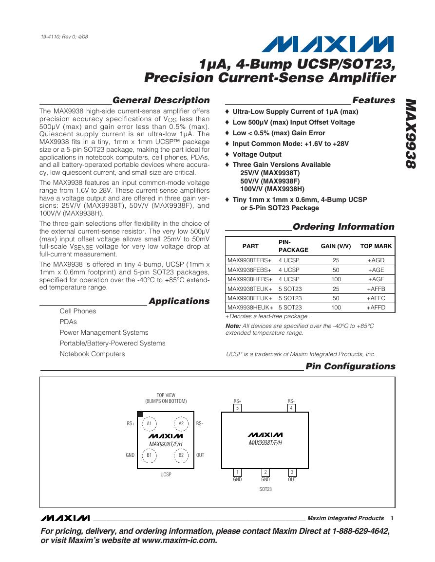
The MAX9938 high-side current-sense amplifier offers
precision accuracy specifications of VOS less than
500μV (max) and gain error less than 0.5% (max).
Quiescent supply current is an ultra-low 1μA. The
MAX9938 fits in a tiny, 1mm x 1mm UCSP™ package
size or a 5-pin SOT23 package, making the part ideal for
applications in notebook computers, cell phones, PDAs,
and all battery-operated portable devices where accura-
cy, low quiescent current, and small size are critical.
The MAX9938 features an input common-mode voltage
range from 1.6V to 28V. These current-sense amplifiers
have a voltage output and are offered in three gain ver-
sions: 25V/V (MAX9938T), 50V/V (MAX9938F), and
100V/V (MAX9938H).
The three gain selections offer flexibility in the choice of
the external current-sense resistor. The very low 500μV
(max) input offset voltage allows small 25mV to 50mV
full-scale VSENSE voltage for very low voltage drop at
full-current measurement.
The MAX9938 is offered in tiny 4-bump, UCSP (1mm x
1mm x 0.6mm footprint) and 5-pin SOT23 packages,
specified for operation over the -40°C to +85°C extend-
ed temperature range.
Applications
Cell Phones
PDAs
Power Management Systems
Portable/Battery-Powered Systems
Notebook Computers
Features
o Ultra-Low Supply Current of 1µA (max)
o Low 500µV (max) Input Offset Voltage
o Low < 0.5% (max) Gain Error
o Input Common Mode: +1.6V to +28V
o Voltage Output
o Three Gain Versions Available
25V/V (MAX9938T)
50V/V (MAX9938F)
100V/V (MAX9938H)
o Tiny 1mm x 1mm x 0.6mm, 4-Bump UCSP
or 5-Pin SOT23 Package
M
A
X
9
9
3
8
Ordering Information
PART
PIN-
PACKAGE
GAIN (V/V)
TOP MARK
MAX9938TEBS+ 4 UCSP
MAX9938FEBS+ 4 UCSP
MAX9938HEBS+ 4 UCSP
MAX9938TEUK+ 5 SOT23
MAX9938FEUK+ 5 SOT23
MAX9938HEUK+ 5 SOT23
+Denotes a lead-free package.
Note:All devices are specified over the -40°C to +85°C
extended temperature range.
25
50
100
25
50
100
+AGD
+AGE
+AGF
+AFFB
+AFFC
+AFFD
UCSP is a trademark of Maxim Integrated Products, Inc.
Pin Configurations
TOP VIEW
(BUMPS ON BOTTOM)
RS+
5
RS-
4
RS+
A1
A2
RS-
MAX9938T/F/H
MAX9938T/F/H
GND
B1
B2
OUT
UCSP
1
GND
2
GND
SOT23
3
OUT
________________________________________________________________ Maxim Integrated Products 1
For pricing, delivery, and ordering information,please contact Maxim Directat 1-888-629-4642,
or visit Maxim’s website at www.maxim-ic.com.
�
8
3
9
9
X
A
M
1µA, 4-Bump UCSP/SOT23,
Precision Current-Sense Amplifier
ABSOLUTE MAXIMUM RATINGS
RS+, RS- to GND....................................................-0.3V to +30V
OUT to GND .............................................................-0.3V to +6V
RS+ to RS- ...........................................................................±30V
Short-Circuit Duration: OUT to GND ..........................Continuous
Continuous Input Current (Any Pin)..................................±20mA
Continuous Power Dissipation (TA = +70°C)
4-Bump UCSP (derate 3.0mW/°C above +70°C).........238mW
5-Pin SOT23 (derate 3.9mW/°C above +70°C)............312mW
Operating Temperature Range ...........................-40°C to +85°C
Junction Temperature......................................................+150°C
Storage Temperature Range ............................-65°C to +150°C
Bump Temperature (soldering) Reflow............................+235°C
Lead Temperature (soldering, 10s) .................................+300°C
Stresses beyond those listed under “Absolute Maximum Ratings” may cause permanent damage to the device. These are stress ratings only, and functional
operation of the device at these or any other conditions beyond those indicated in the operational sections of the specifications is not implied. Exposure to
absolute maximum rating conditions for extended periods may affect device reliability.
ELECTRICAL CHARACTERISTICS
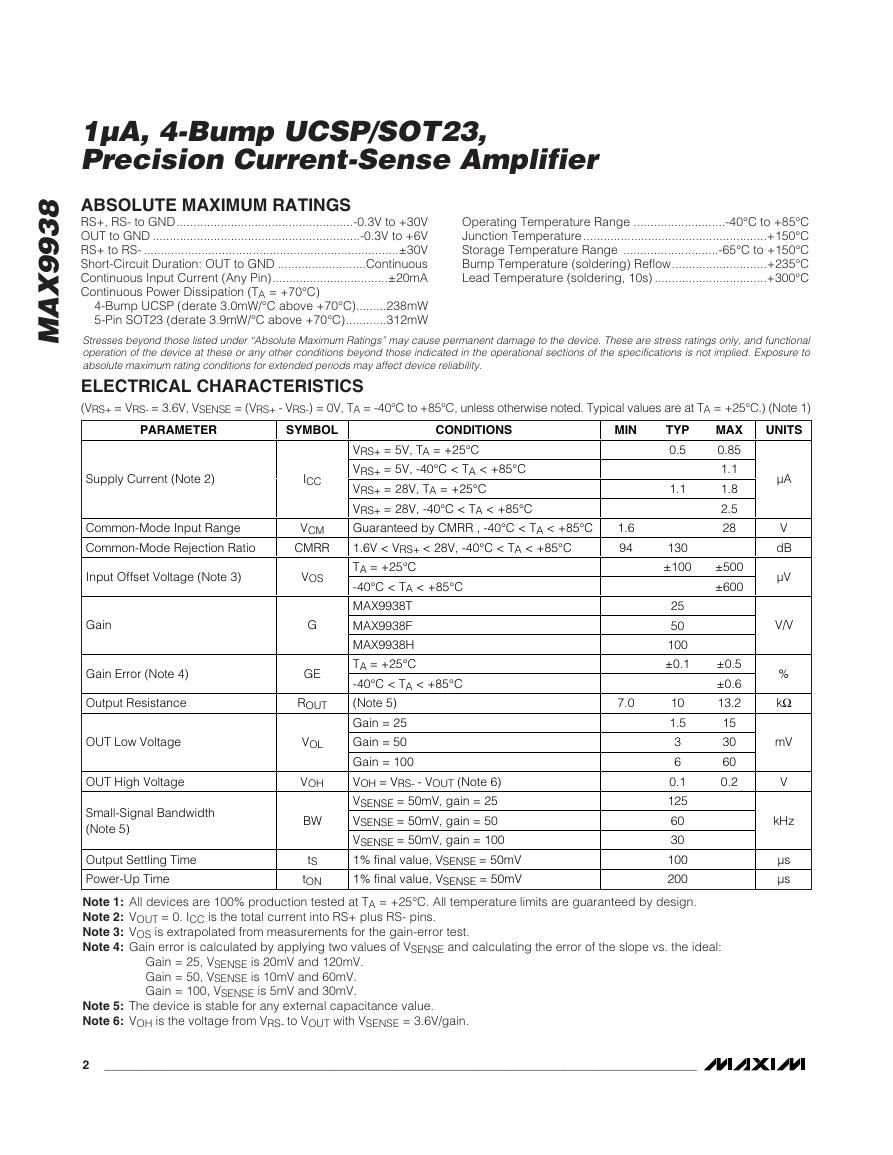
(VRS+ = VRS- = 3.6V, VSENSE = (VRS+ - VRS-) = 0V, TA = -40°C to +85°C, unless otherwise noted. Typical values are at TA = +25°C.) (Note 1)
PARAMETER
SYMBOL
CONDITIONS
MIN
Supply Current (Note 2)
Common-Mode Input Range
Common-Mode Rejection Ratio
Input Offset Voltage (Note 3)
Gain
Gain Error (Note 4)
Output Resistance
OUT Low Voltage
OUT High Voltage
Small-Signal Bandwidth
(Note 5)
Output Settling Time
Power-Up Time
VRS+ = 5V, TA = +25°C
VRS+ = 5V, -40°C < TA < +85°C
VRS+ = 28V, TA = +25°C
VRS+ = 28V, -40°C < TA < +85°C
Guaranteed by CMRR , -40°C < TA < +85°C
1.6V < VRS+ < 28V, -40°C < TA < +85°C
TA = +25°C
-40°C < TA < +85°C
MAX9938T
MAX9938F
MAX9938H
TA = +25°C
-40°C < TA < +85°C
(Note 5)
Gain = 25
Gain = 50
Gain = 100
VOH = VRS- - VOUT (Note 6)
VSENSE = 50mV, gain = 25
VSENSE = 50mV, gain = 50
VSENSE = 50mV, gain = 100
1% final value, VSENSE = 50mV
1% final value, VSENSE = 50mV
ICC
VCM
CMRR
VOS
G
GE
ROUT
VOL
VOH
BW
tS
tON
1.6
94
7.0
TYP
0.5
1.1
130
±100
25
50
100
±0.1
10
1.5
3
6
0.1
125
60
30
100
200
MAX
0.85
1.1
1.8
2.5
28
±500
±600
±0.5
±0.6
13.2
15
30
60
0.2
UNITS
μA
V
dB
μV
V/V
%
kΩ
mV
V
kHz
μs
μs
Note 1: All devices are 100% production tested at TA = +25°C. All temperature limits are guaranteed by design.
Note 2: VOUT = 0. ICC is the total current into RS+ plus RS- pins.
Note 3: VOS is extrapolated from measurements for the gain-error test.
Note 4: Gain error is calculated by applying two values of VSENSE and calculating the error of the slope vs. the ideal:
Gain = 25, VSENSE is 20mV and 120mV.
Gain = 50, VSENSE is 10mV and 60mV.
Gain = 100, VSENSE is 5mV and 30mV.
Note 5: The device is stable for any external capacitance value.
Note 6: VOH is the voltage from VRS- to VOUT with VSENSE = 3.6V/gain.
2
_______________________________________________________________________________________
�
M
A
X
9
9
3
8
1µA, 4-Bump UCSP/SOT23,
Precision Current-Sense Amplifier
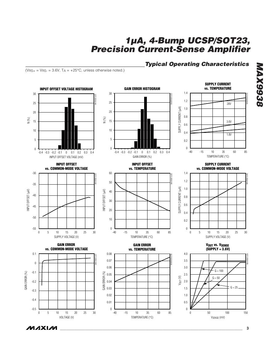
Typical Operating Characteristics
(VRS+ = VRS- = 3.6V, TA = +25°C, unless otherwise noted.)
INPUT OFFSET VOLTAGE HISTOGRAM
GAIN ERROR HISTOGRAM
30
25
20
15
10
5
0
-30
-35
-40
-45
-50
-55
0.1
0
-0.1
-0.2
-0.3
-0.4
-0.5
)
%
(
N
)
V
μ
(
T
E
S
F
F
O
T
U
P
N
I
)
%
(
R
O
R
R
E
N
A
G
I
30
25
20
15
10
5
0
60
50
40
30
20
10
0
)
%
(
N
)
V
μ
(
T
E
S
F
F
O
T
U
P
N
I
1
0
c
o
t
8
3
9
9
X
A
M
4
0
c
o
t
8
3
9
9
X
A
M
-0.4 -0.3 -0.2 -0.1
0
0.1
0.2
0.3
0.4
INPUT OFFSET VOLTAGE (mV)
INPUT OFFSET
vs. COMMON-MODE VOLTAGE
0
5
15
10
20
SUPPLY VOLTAGE (V)
25
30
GAIN ERROR
vs. COMMON-MODE VOLTAGE
7
0
c
o
t
8
3
9
9
X
A
M
0.08
0.07
0.06
0.05
0.04
0.03
0.02
0.01
)
%
(
R
O
R
R
E
N
A
G
I
-0.4 -0.3 -0.2 -0.1
0
0.1
GAIN ERROR (%)
0.2
0.3
0.4
INPUT OFFSET
vs. TEMPERATURE
2
0
c
o
t
8
3
9
9
X
A
M
5
0
c
o
t
8
3
9
9
X
A
M
)
A
μ
(
T
N
E
R
R
U
C
Y
L
P
P
U
S
)
A
μ
(
T
N
E
R
R
U
C
Y
L
P
P
U
S
-40
-15
10
35
60
85
TEMPERATURE (°C)
GAIN ERROR
vs. TEMPERATURE
8
0
c
o
t
8
3
9
9
X
A
M
)
V
(
T
U
O
V
0
5
10
15
20
25
30
VOLTAGE (V)
0
-40
-15
10
35
60
85
TEMPERATURE (°C)
1.4
1.2
1.0
0.8
0.6
0.4
0.2
0
1.4
1.2
1.0
0.8
0.6
0.4
0.2
0
4.0
3.5
3.0
2.5
2.0
1.5
1.0
0.5
0
SUPPLY CURRENT
vs. TEMPERATURE
3
0
c
o
t
8
3
9
9
X
A
M
28V
3.6V
1.8V
-40
-15
10
35
60
85
TEMPERATURE (°C)
SUPPLY CURRENT
vs. COMMON-MODE VOLTAGE
6
0
c
o
t
8
3
9
9
X
A
M
0
5
15
10
20
SUPPLY VOLTAGE (V)
25
30
VOUT vs. VSENSE
(SUPPLY = 3.6V)
9
0
c
o
t
8
3
9
9
X
A
M
G = 100
G = 50
G = 25
0
50
100
150
VSENSE (mV)
_______________________________________________________________________________________ 3
�
1µA, 4-Bump UCSP/SOT23,
Precision Current-Sense Amplifier
8
3
9
9
X
A
M
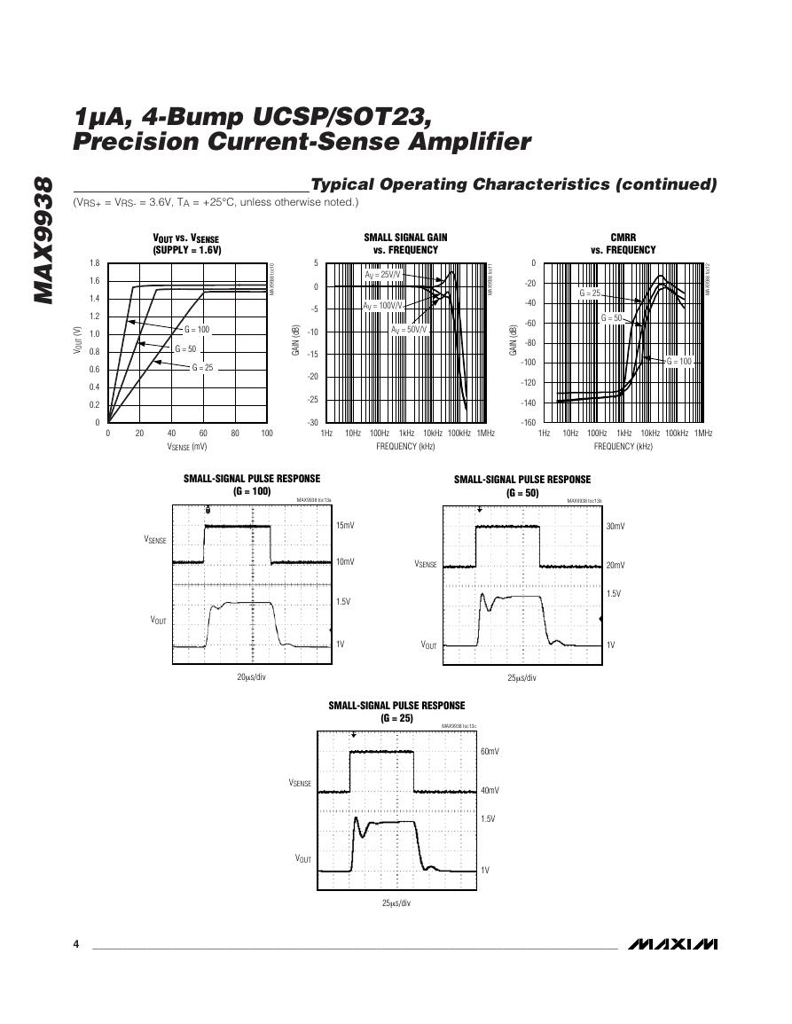
(VRS+ = VRS- = 3.6V, TA = +25°C, unless otherwise noted.)
Typical Operating Characteristics (continued)
)
V
(
T
U
O
V
1.8
1.6
1.4
1.2
1.0
0.8
0.6
0.4
0.2
0
VOUT vs. VSENSE
(SUPPLY = 1.6V)
G = 100
G = 50
G = 25
0
1
c
o
t
8
3
9
9
X
A
M
)
B
d
(
I
N
A
G
0
20
40
60
VSENSE (mV)
80
100
5
0
-5
-10
-15
-20
-25
-30
SMALL SIGNAL GAIN
vs. FREQUENCY
AV = 25V/V
AV = 100V/V
AV = 50V/V
1
1
c
o
t
8
3
9
9
X
A
M
1Hz
10Hz
100Hz
1kHz
10kHz
100kHz
1MHz
FREQUENCY (kHz)
)
B
d
(
I
N
A
G
0
-20
-40
-60
-80
-100
-120
-140
-160
CMRR
vs. FREQUENCY
G = 25
G = 50
2
1
c
o
t
8
3
9
9
X
A
M
G = 100
1Hz
10Hz
100Hz
1kHz
10kHz
100kHz
1MHz
FREQUENCY (kHz)
SMALL-SIGNAL PULSE RESPONSE
(G = 100)
MAX9938 toc13a
15mV
10mV
1.5V
1V
VSENSE
VOUT
VSENSE
VOUT
SMALL-SIGNAL PULSE RESPONSE
(G = 50)
MAX9938 toc13b
30mV
20mV
1.5V
1V
20μs/div
25μs/div
SMALL-SIGNAL PULSE RESPONSE
(G = 25)
MAX9938 toc13c
60mV
40mV
1.5V
1V
VSENSE
VOUT
25μs/div
4
_______________________________________________________________________________________
�
1µA, 4-Bump UCSP/SOT23,
Precision Current-Sense Amplifier
Typical Operating Characteristics (continued)
(VRS+ = VRS- = 3.6V, TA = +25°C, unless otherwise noted.)
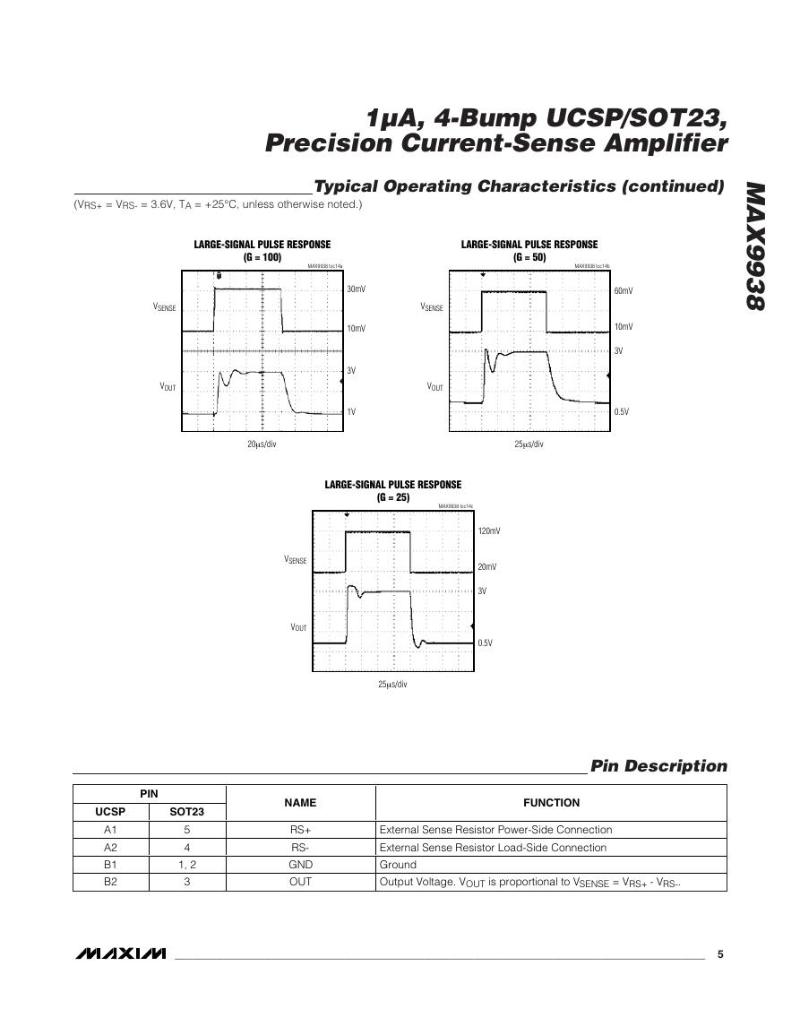
LARGE-SIGNAL PULSE RESPONSE
(G = 100)
M
A
X
9
9
3
8
MAX9938 toc14a
30mV
10mV
3V
1V
VSENSE
VOUT
LARGE-SIGNAL PULSE RESPONSE
(G = 50)
MAX9938 toc14b
60mV
10mV
3V
0.5V
20μs/div
25μs/div
LARGE-SIGNAL PULSE RESPONSE
(G = 25)
MAX9938 toc14c
120mV
20mV
3V
0.5V
25μs/div
Pin Description
FUNCTION
External Sense Resistor Power-Side Connection
External Sense Resistor Load-Side Connection
Ground
Output Voltage. VOUT is proportional to VSENSE = VRS+ - VRS-.
VSENSE
VOUT
NAME
RS+
RS-
GND
OUT
VSENSE
VOUT
PIN
UCSP
SOT23
A1
A2
B1
B2
5
4
1, 2
3
_______________________________________________________________________________________ 5
�
1µA, 4-Bump UCSP/SOT23,
Precision Current-Sense Amplifier
8
3
9
9
X
A
M
VBATT = 1.6V TO 28V
ILOAD
RSENSE
RS+
R1
RS-
R1
Typical Operating Circuit
VDD = 3.3V
LOAD
MAX9938
OUT
μC
ADC
P
ROUT
10kΩ
GND
Detailed Description
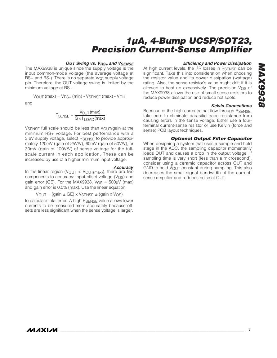
The MAX9938 unidirectional high-side, current-sense
amplifier features a 1.6V to 28V input common-mode
range. This feature allows the monitoring of current out
of a battery with a voltage as low as 1.6V. The
MAX9938 monitors current through a current-sense
resistor and amplifies the voltage across that resistor.
The MAX9938 is a unidirectional current-sense amplifier
that has a well-established history. An op amp is used
to force the current through an internal gain resistor at
RS+, which has a value of R1, such that its voltage drop
equals the voltage drop across an external sense resis-
tor, RSENSE. There is an internal resistor at RS- with the
Table 1. Internal Gain Setting Resistors
(Typical Values)
GAIN
(V/V)
100
50
25
R1
(Ω)
100
200
400
ROUT
(kΩ)
10
10
10
same value as R1 to minimize offset voltage. The cur-
rent through R1 is sourced by a high-voltage p-channel
FET. Its source current is the same as its drain current,
which flows through a second gain resistor, ROUT. This
produces an output voltage, VOUT, whose magnitude is
ILOAD x RSENSE x ROUT/R1. The gain accuracy is
based on the matching of the two gain resistors R1 and
ROUT (see Table 1). Total gain = 25V/V for the
MAX9938T, 50V/V for the MAX9938F, and 100V/V for
the MAX9938H. The output is protected from input
overdrive by use of an output current limiting circuit of
7mA (typical) and a 6V clamp protection circuit.
Applications Information
Choosing the Sense Resistor
Choose RSENSE based on the following criteria:
Voltage Loss
A high RSENSE value causes the power-source voltage
to drop due to IR loss. For minimal voltage loss, use the
lowest RSENSE value.
6
_______________________________________________________________________________________
�
1µA, 4-Bump UCSP/SOT23,
Precision Current-Sense Amplifier
OUT Swing vs. VRS+and VSENSE
The MAX9938 is unique since the supply voltage is the
input common-mode voltage (the average voltage at
RS+ and RS-). There is no separate VCC supply voltage
pin. Therefore, the OUT voltage swing is limited by the
minimum voltage at RS+.
VOUT (max) = VRS+ (min) - VSENSE (max) - VOH
and
R
SENSE
=
(max)
V
OUT
×
G I
LOAD
(max)
VSENSE full scale should be less than VOUT/gain at the
minimum RS+ voltage. For best performance with a
3.6V supply voltage, select RSENSE to provide approxi-
mately 120mV (gain of 25V/V), 60mV (gain of 50V/V), or
30mV (gain of 100V/V) of sense voltage for the full-
scale current in each application. These can be
increased by use of a higher minimum input voltage.
Accuracy
In the linear region (VOUT < VOUT(max)), there are two
components to accuracy: input offset voltage (VOS) and
gain error (GE). For the MAX9938, VOS = 500μV (max)
and gain error is 0.5% (max). Use the linear equation:
VOUT = (gain ± GE) x VSENSE ± (gain x VOS)
to calculate total error. A high RSENSE value allows lower
currents to be measured more accurately because off-
sets are less significant when the sense voltage is larger.
M
A
X
9
9
3
8
Efficiency and Power Dissipation
At high current levels, the I2R losses in RSENSE can be
significant. Take this into consideration when choosing
the resistor value and its power dissipation (wattage)
rating. Also, the sense resistor’s value might drift if it is
allowed to heat up excessively. The precision VOS of
the MAX9938 allows the use of small sense resistors to
reduce power dissipation and reduce hot spots.
Kelvin Connections
Because of the high currents that flow through RSENSE,
take care to eliminate parasitic trace resistance from
causing errors in the sense voltage. Either use a four-
terminal current-sense resistor or use Kelvin (force and
sense) PCB layout techniques.
Optional Output Filter Capacitor
When designing a system that uses a sample-and-hold
stage in the ADC, the sampling capacitor momentarily
loads OUT and causes a drop in the output voltage. If
sampling time is very short (less than a microsecond),
consider using a ceramic capacitor across OUT and
GND to hold VOUT constant during sampling. This also
decreases the small-signal bandwidth of the current-
sense amplifier and reduces noise at OUT.
_______________________________________________________________________________________ 7
�
1µA, 4-Bump UCSP/SOT23,
Precision Current-Sense Amplifier
8
3
9
9
X
A
M
ILOAD
RSENSE
VBATT = 1.6V TO 28V
TO WALL-CUBE/
CHARGER
RS+
R1
RS-
R1
RS+
R1
RS-
R1
LOAD
P
P
MAX9938
OUT
MAX9938
VDD = 3.3V
OUT
ROUT
10kΩ
GND
ROUT
10kΩ
GND
μC
ADC
ADC
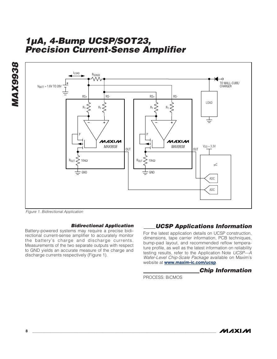
Figure 1. Bidirectional Application
Bidirectional Application
Battery-powered systems may require a precise bidi-
rectional current-sense amplifier to accurately monitor
the battery’s charge and discharge currents.
Measurements of the two separate outputs with respect
to GND yields an accurate measure of the charge and
discharge currents respectively (Figure 1).
UCSP Applications Information
For the latest application details on UCSP construction,
dimensions, tape carrier information, PCB techniques,
bump-pad layout, and recommended reflow tempera-
ture profile, as well as the latest information on reliability
testing results, refer to the Application Note UCSP—A
Wafer-Level Chip-Scale Package available on Maxim’s
website at www.maxim-ic.com/ucsp.
Chip Information
PROCESS: BiCMOS
8
_______________________________________________________________________________________
�


 V2版本原理图(Capacitive-Fingerprint-Reader-Schematic_V2).pdf
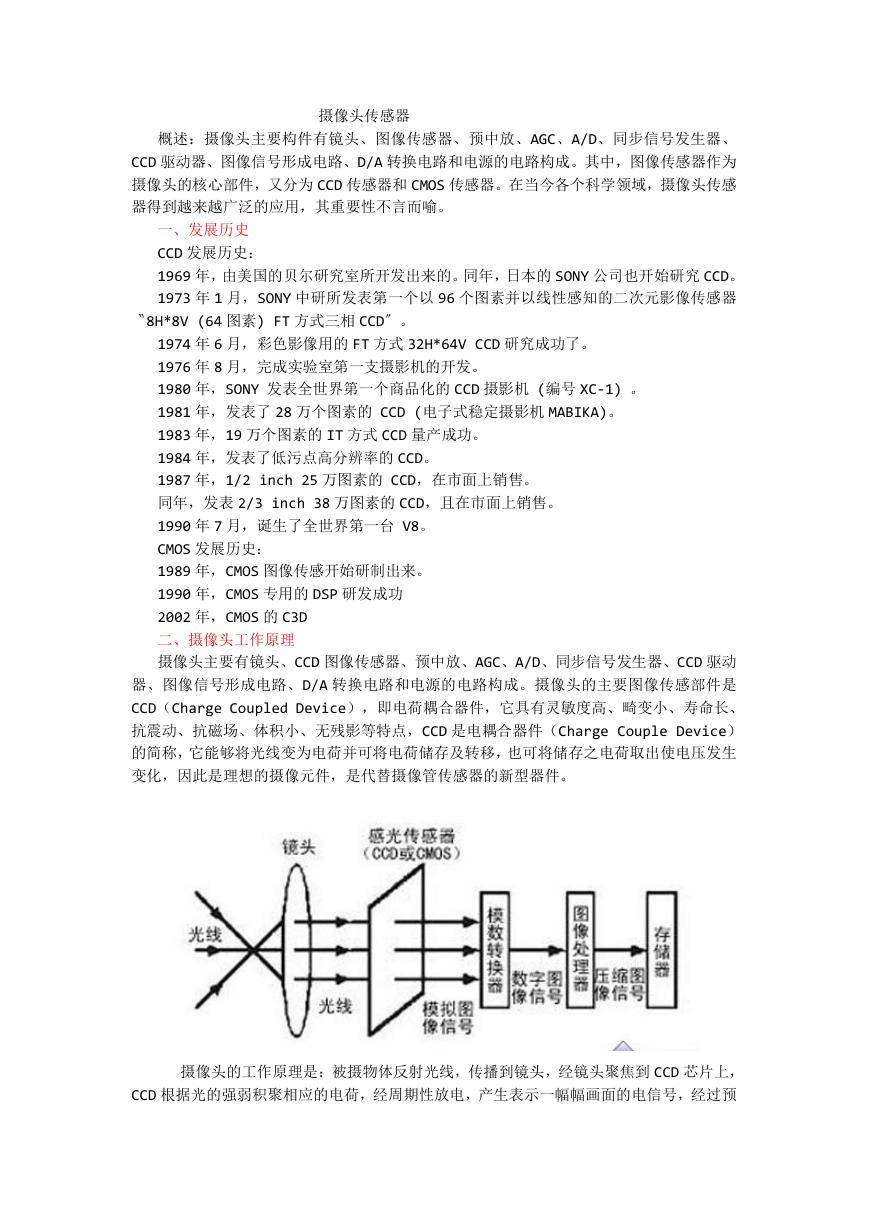 摄像头工作原理.doc
 VL53L0X简要说明(En.FLVL53L00216).pdf
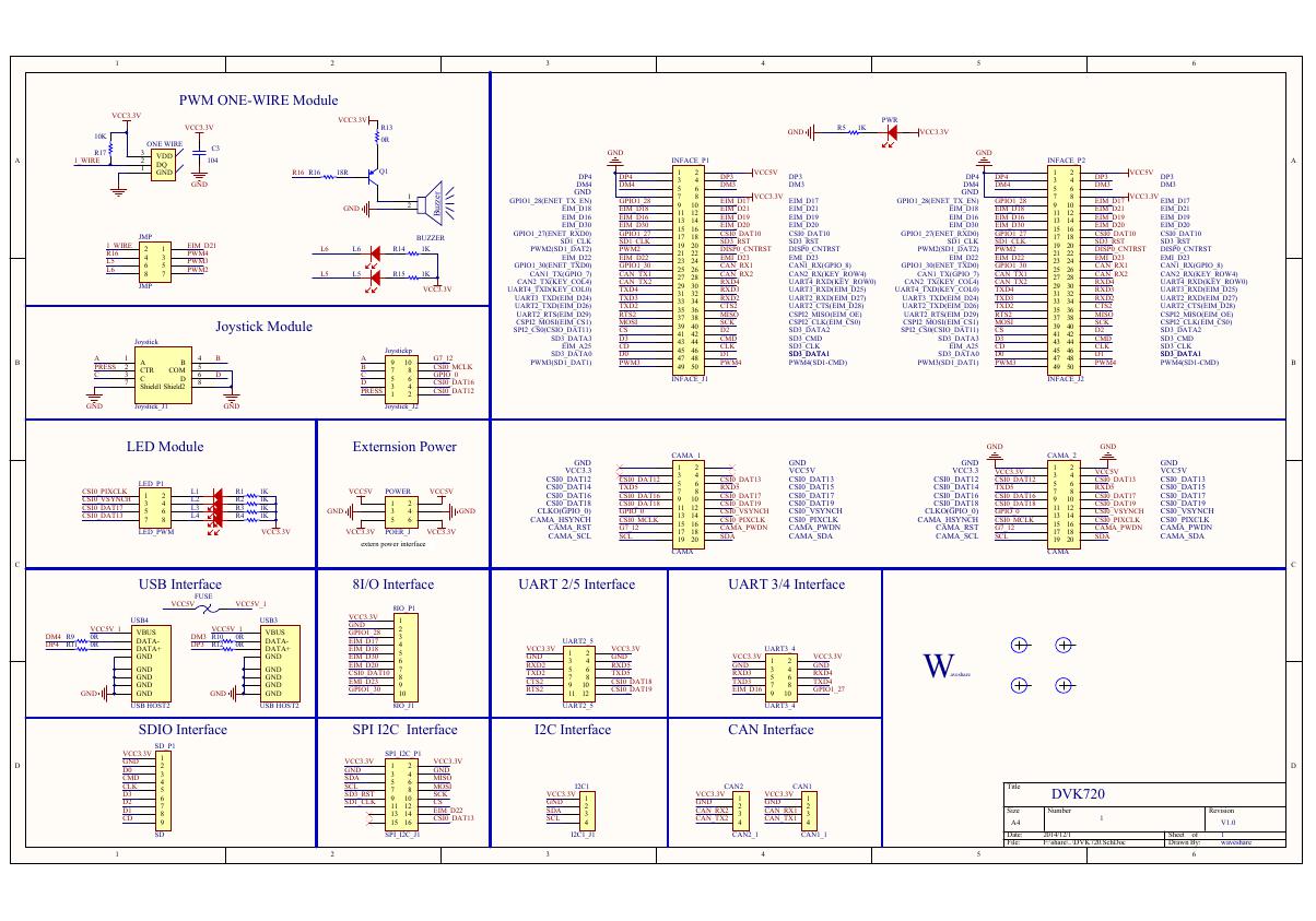 原理图(DVK720-Schematic).pdf
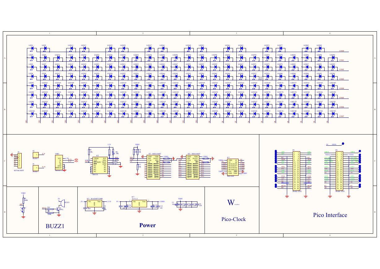 原理图(Pico-Clock-Green-Schdoc).pdf
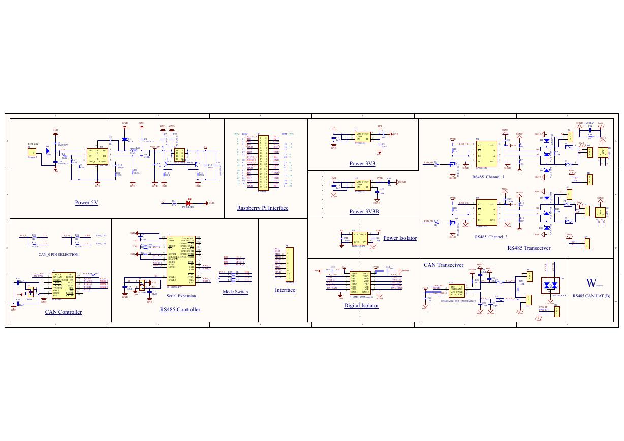 原理图(RS485-CAN-HAT-B-schematic).pdf
 File:SIM7500_SIM7600_SIM7800 Series_SSL_Application Note_V2.00.pdf
 ADS1263(Ads1262).pdf
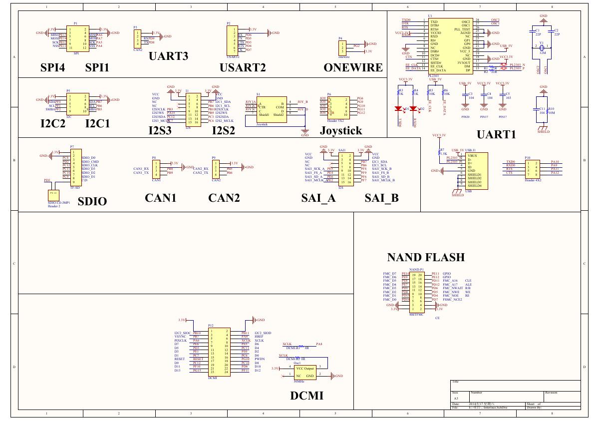 原理图(Open429Z-D-Schematic).pdf
 用户手册(Capacitive_Fingerprint_Reader_User_Manual_CN).pdf
 CY7C68013A(英文版)(CY7C68013A).pdf
 TechnicalReference_Dem.pdf