DATA SHEET
NVIDIA Jetson Orin NX Series
Ampere GPU + Arm® Cortex®-A78AE CPU + LPDDR5
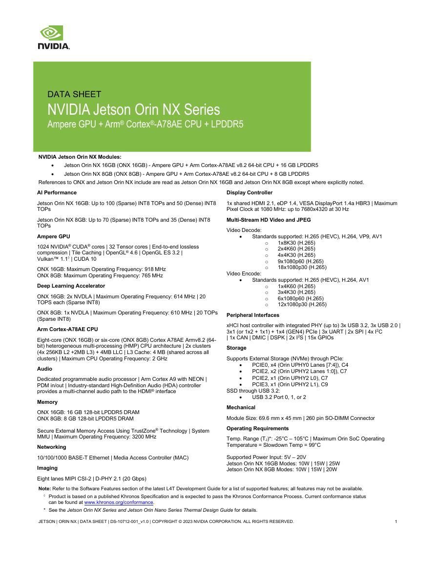
NVIDIA Jetson Orin NX Modules:
•
•
Jetson Orin NX 16GB (ONX 16GB) - Ampere GPU + Arm Cortex-A78AE v8.2 64-bit CPU + 16 GB LPDDR5
Jetson Orin NX 8GB (ONX 8GB) - Ampere GPU + Arm Cortex-A78AE v8.2 64-bit CPU + 8 GB LPDDR5
Video Encode:
•
Standards supported: H.265 (HEVC), H.264, AV1
1x4K60 (H.265)
3x4K30 (H.265)
6x1080p60 (H.265)
12x1080p30 (H.265)
1x8K30 (H.265)
2x4K60 (H.265)
4x4K30 (H.265)
9x1080p60 (H.265)
18x1080p30 (H.265)
Display Controller
1x shared HDMI 2.1, eDP 1.4, VESA DisplayPort 1.4a HBR3 | Maximum
Pixel Clock at 1080 MHz: up to 7680x4320 at 30 Hz
Multi-Stream HD Video and JPEG
Video Decode:
References to ONX and Jetson Orin NX include are read as Jetson Orin NX 16GB and Jetson Orin NX 8GB except where explicitly noted.
AI Performance
Jetson Orin NX 16GB: Up to 100 (Sparse) INT8 TOPs and 50 (Dense) INT8
TOPs
Jetson Orin NX 8GB: Up to 70 (Sparse) INT8 TOPs and 35 (Dense) INT8
TOPs
Ampere GPU
1024 NVIDIA® CUDA® cores | 32 Tensor cores | End-to-end lossless
compression | Tile Caching | OpenGL® 4.6 | OpenGL ES 3.2 |
Vulkan™ 1.1◊ | CUDA 10
ONX 16GB: Maximum Operating Frequency: 918 MHz
ONX 8GB: Maximum Operating Frequency: 765 MHz
Deep Learning Accelerator
ONX 16GB: 2x NVDLA | Maximum Operating Frequency: 614 MHz | 20
TOPS each (Sparse INT8)
ONX 8GB: 1x NVDLA | Maximum Operating Frequency: 610 MHz | 20 TOPs
(Sparse INT8)
Arm Cortex-A78AE CPU
Eight-core (ONX 16GB) or six-core (ONX 8GB) Cortex A78AE Armv8.2 (64-
bit) heterogeneous multi-processing (HMP) CPU architecture | 2x clusters
(4x 256KB L2 +2MB L3) + 4MB LLC | L3 Cache: 4 MB (shared across all
clusters) | Maximum CPU Operating Frequency: 2 GHz
Audio
Dedicated programmable audio processor | Arm Cortex A9 with NEON |
PDM in/out | Industry-standard High-Definition Audio (HDA) controller
provides a multi-channel audio path to the HDMI® interface
Memory
ONX 16GB: 16 GB 128-bit LPDDR5 DRAM
ONX 8GB: 8 GB 128-bit LPDDR5 DRAM
Secure External Memory Access Using TrustZone® Technology | System
MMU | Maximum Operating Frequency: 3200 MHz
Networking
10/100/1000 BASE-T Ethernet | Media Access Controller (MAC)
Imaging
Eight lanes MIPI CSI-2 | D-PHY 2.1 (20 Gbps)
Note: Refer to the Software Features section of the latest L4T Development Guide for a list of supported features; all features may not be available.
◊ Product is based on a published Khronos Specification and is expected to pass the Khronos Conformance Process. Current conformance status
can be found at www.khronos.org/conformance.
* See the Jetson Orin NX Series and Jetson Orin Nano Series Thermal Design Guide for details.
Mechanical
Module Size: 69.6 mm x 45 mm | 260 pin SO-DIMM Connector
Operating Requirements
Temp. Range (TJ)*: -25°C – 105°C | Maximum Orin SoC Operating
Temperature = Slowdown Temp = 99°C
Supported Power Input: 5V – 20V
Jetson Orin NX 16GB Modes: 10W | 15W | 25W
Jetson Orin NX 8GB Modes: 10W | 15W | 20W
Peripheral Interfaces
xHCI host controller with integrated PHY (up to) 3x USB 3.2, 3x USB 2.0 |
3x1 (or 1x2 + 1x1) + 1x4 (GEN4) PCIe | 3x UART | 2x SPI | 4x I2C
| 1x CAN | DMIC | DSPK | 2x I2S | 15x GPIOs
Storage
Supports External Storage (NVMe) through PCIe:
PCIE0, x4 (Orin UPHY0 Lanes [7:4]), C4
PCIE2, x2 (Orin UPHY2 Lanes 1:0]), C7
PCIE2, x1 (Orin UPHY2 L0), C7
PCIE3, x1 (Orin UPHY2 L1), C9
SSD through USB 3.2:
USB 3.2 Port 0, 1, or 2
•
Standards supported: H.265 (HEVC), H.264, VP9, AV1
o
o
o
o
o
o
o
o
o
•
•
•
•
•
JETSON | ORIN NX | DATA SHEET | DS-10712-001_v1.0 | COPYRIGHT © 2023 NVIDIA CORPORATION. ALL RIGHTS RESERVED.
1
�
Jetson Orin NX System-on-Module
Ampere GPU + A78AE Cortex CPU + LPDDR5
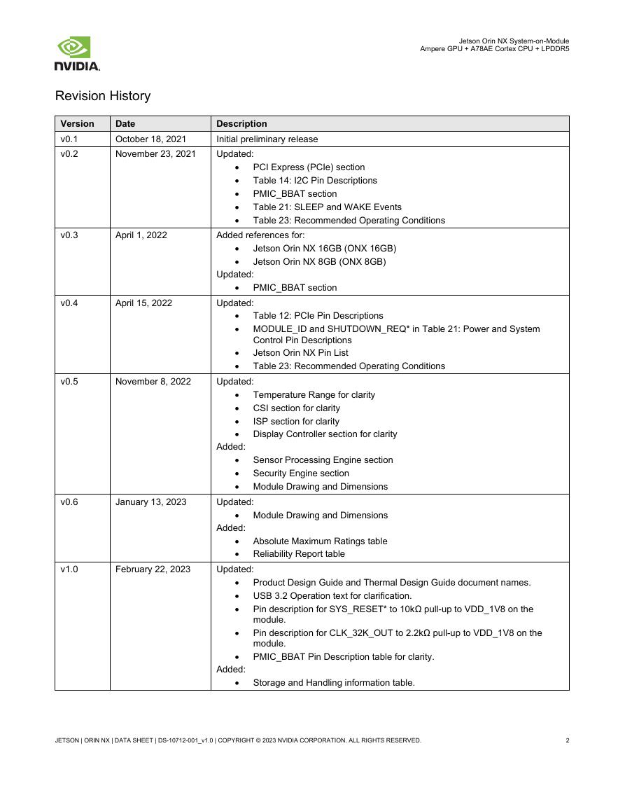
Revision History
Version
v0.1
v0.2
Date
October 18, 2021
November 23, 2021
Description
Initial preliminary release
Updated:
Table 14: I2C Pin Descriptions
• PCI Express (PCIe) section
•
• PMIC_BBAT section
•
•
Table 21: SLEEP and WAKE Events
Table 23: Recommended Operating Conditions
v0.3
April 1, 2022
Added references for:
•
•
Jetson Orin NX 16GB (ONX 16GB)
Jetson Orin NX 8GB (ONX 8GB)
Updated:
• PMIC_BBAT section
v0.4
April 15, 2022
Updated:
Table 12: PCIe Pin Descriptions
•
• MODULE_ID and SHUTDOWN_REQ* in Table 21: Power and System
Control Pin Descriptions
Jetson Orin NX Pin List
Table 23: Recommended Operating Conditions
•
•
v0.5
November 8, 2022
Updated:
Temperature Range for clarity
•
• CSI section for clarity
•
ISP section for clarity
• Display Controller section for clarity
Added:
• Sensor Processing Engine section
• Security Engine section
• Module Drawing and Dimensions
v0.6
January 13, 2023
Updated:
• Module Drawing and Dimensions
Added:
• Absolute Maximum Ratings table
• Reliability Report table
v1.0
February 22, 2023
Updated:
• Product Design Guide and Thermal Design Guide document names.
• USB 3.2 Operation text for clarification.
• Pin description for SYS_RESET* to 10kΩ pull-up to VDD_1V8 on the
module.
• Pin description for CLK_32K_OUT to 2.2kΩ pull-up to VDD_1V8 on the
module.
• PMIC_BBAT Pin Description table for clarity.
Added:
• Storage and Handling information table.
JETSON | ORIN NX | DATA SHEET | DS-10712-001_v1.0 | COPYRIGHT © 2023 NVIDIA CORPORATION. ALL RIGHTS RESERVED.
2
�
Jetson Orin NX System-on-Module
Ampere GPU + A78AE Cortex CPU + LPDDR5
Table of Contents
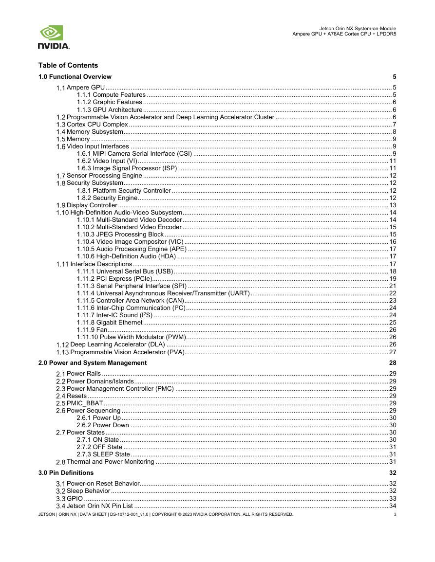
1.0 Functional Overview
5
Ampere GPU ................................................................................................................................................................ 5
1.1.1 Compute Features ......................................................................................................................................... 5
1.1.2 Graphic Features ........................................................................................................................................... 6
1.1.3 GPU Architecture ........................................................................................................................................... 6
Programmable Vision Accelerator and Deep Learning Accelerator Cluster ................................................................. 6
Cortex CPU Complex ................................................................................................................................................... 7
Memory Subsystem ...................................................................................................................................................... 8
Memory ........................................................................................................................................................................ 9
Video Input Interfaces .................................................................................................................................................. 9
1.6.1 MIPI Camera Serial Interface (CSI) ............................................................................................................... 9
1.6.2 Video Input (VI) ............................................................................................................................................ 11
1.6.3 Image Signal Processor (ISP) ...................................................................................................................... 11
Sensor Processing Engine ......................................................................................................................................... 12
Security Subsystem .................................................................................................................................................... 12
1.8.1 Platform Security Controller ......................................................................................................................... 12
1.8.2 Security Engine ............................................................................................................................................ 12
Display Controller ....................................................................................................................................................... 13
High-Definition Audio-Video Subsystem ................................................................................................................... 14
1.10.1 Multi-Standard Video Decoder ................................................................................................................... 14
1.10.2 Multi-Standard Video Encoder ................................................................................................................... 15
1.10.3 JPEG Processing Block ............................................................................................................................. 15
1.10.4 Video Image Compositor (VIC) .................................................................................................................. 16
1.10.5 Audio Processing Engine (APE) ................................................................................................................ 17
1.10.6 High-Definition Audio (HDA) ...................................................................................................................... 17
Interface Descriptions ............................................................................................................................................... 17
1.11.1 Universal Serial Bus (USB) ........................................................................................................................ 18
1.11.2 PCI Express (PCIe) .................................................................................................................................... 19
1.11.3 Serial Peripheral Interface (SPI) ................................................................................................................ 21
1.11.4 Universal Asynchronous Receiver/Transmitter (UART) ............................................................................. 22
1.11.5 Controller Area Network (CAN) .................................................................................................................. 23
1.11.6 Inter-Chip Communication (I2C) ................................................................................................................. 24
1.11.7 Inter-IC Sound (I2S) ................................................................................................................................... 24
1.11.8 Gigabit Ethernet ......................................................................................................................................... 25
1.11.9 Fan ............................................................................................................................................................. 26
1.11.10 Pulse Width Modulator (PWM) ................................................................................................................. 26
Deep Learning Accelerator (DLA) ............................................................................................................................ 26
Programmable Vision Accelerator (PVA).................................................................................................................. 27
28
Power Rails ................................................................................................................................................................ 29
Power Domains/Islands .............................................................................................................................................. 29
Power Management Controller (PMC) ....................................................................................................................... 29
Resets ........................................................................................................................................................................ 29
PMIC_BBAT ............................................................................................................................................................... 29
Power Sequencing ..................................................................................................................................................... 29
2.6.1 Power Up ..................................................................................................................................................... 30
2.6.2 Power Down ................................................................................................................................................ 30
Power States .............................................................................................................................................................. 30
2.7.1 ON State ...................................................................................................................................................... 30
2.7.2 OFF State .................................................................................................................................................... 31
2.7.3 SLEEP State ................................................................................................................................................ 31
Thermal and Power Monitoring .................................................................................................................................. 31
32
Power-on Reset Behavior........................................................................................................................................... 32
Sleep Behavior ........................................................................................................................................................... 32
GPIO .......................................................................................................................................................................... 33
Jetson Orin NX Pin List .............................................................................................................................................. 34
3
2.0 Power and System Management
3.0 Pin Definitions
JETSON | ORIN NX | DATA SHEET | DS-10712-001_v1.0 | COPYRIGHT © 2023 NVIDIA CORPORATION. ALL RIGHTS RESERVED.
�
Jetson Orin NX System-on-Module
Ampere GPU + A78AE Cortex CPU + LPDDR5
4.0 DC Characteristics
37
Operating and Absolute Maximum Ratings ................................................................................................................ 37
Storage and Handling ................................................................................................................................................. 38
Digital Logic ................................................................................................................................................................ 38
39
40
5.0 Environmental and Mechanical Screening
6.0 Module Drawing and Dimensions
JETSON | ORIN NX | DATA SHEET | DS-10712-001_v1.0 | COPYRIGHT © 2023 NVIDIA CORPORATION. ALL RIGHTS RESERVED.
4
�
Jetson Orin NX System-on-Module
Ampere GPU + A78AE Cortex CPU + LPDDR5
1.0 Functional Overview
NVIDIA® Jetson Orin™ NX brings AI supercomputer performance to the edge in a compact system-on-module (SOM) which is
smaller than a credit card. Jetson Orin NX is built around a low-power version of the NVIDIA Orin SoC, combining the NVIDIA
Ampere™ GPU architecture with 64-bit operating capability, integrated advanced multi-function video and image processing,
and NVIDIA Deep Learning Accelerators.
Compute performance up to 100 (Sparse) INT8 TOPs and 50 (Dense) INT8 TOPs enables the Jetson Orin NX to run multiple
neural networks in parallel and process data from multiple high-resolution sensors simultaneously. It also offers a unique
combination of performance and power advantages with a rich set of I/Os, from high-speed CSI and PCIe to low-speed I2Cs
and GPIOs, allowing embedded and edge computing devices that demand increased performance but are constrained by size,
weight, and power budgets.
Ampere GPU
The NVIDIA Ampere GPU introduces a new design for the Streaming Multiprocessor (SM) that dramatically improves
performance per watt and performance per area, along with supporting Tensor Cores and TensorRT Cores. Ampere GPUs
improve on the previous NVIDIA Turing™ generation; and are software compatible so that the same APIs are used.
The NVIDIA Ampere Architecture GPU has several enhancements for compute and graphics capability that include:
2x CUDA floating-point performance: higher compute math speed.
• Sparsity: fine grained structured sparsity doubles throughput and reduces memory usage.
•
• SM architecture improves bandwidth to the L1 cache and shared memory and reduces L1 miss latency.
•
Improved async compute and post-L2 cache compression compared to NVIDIA Turing.
1.1.1 Compute Features
Ampere introduces third-generation NVIDIA Tensor Cores which offer a wider range of precisions including TensorFloat-32
(TF32), bfloat16, FP16, and INT8, all of which provide unmatched versatility and performance.
TensorFloat-32 (TF32) is a new format that uses the same 10-bit Mantissa as half-precision (FP16) math and is shown to have
more than sufficient margin for the precision requirements of AI workloads. In addition, since the TF32 adopts the same 8-bit
exponent as FP32 it can support the same numeric range.
Ampere adds support for structured sparsity. Not all the parameters of modern AI networks are needed for accurate
predictions and inference, some can be converted to zeros to make the models “sparse” without compromising accuracy. The
Tensor Cores in Ampere can provide up to 2x higher performance for inference of sparse models.
Ampere supports Compute Data Compression which can accelerate unstructured sparsity and other compressible data
patterns. Compression in L2 provides up to a 4x improvement in DRAM read/write bandwidth, up to 4x improvement in L2 read
bandwidth, and up to a 2x improvement in L2 capacity.
Ampere also supports many other enhancements for higher compute throughput.
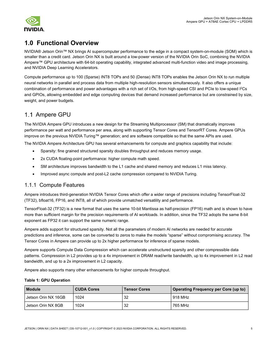
Table 1: GPU Operation
Module
Jetson Orin NX 16GB
Jetson Orin NX 8GB
CUDA Cores
1024
1024
Tensor Cores
32
32
Operating Frequency per Core (up to)
918 MHz
765 MHz
JETSON | ORIN NX | DATA SHEET | DS-10712-001_v1.0 | COPYRIGHT © 2023 NVIDIA CORPORATION. ALL RIGHTS RESERVED.
5
�
1.1.2 Graphic Features
Ampere graphics capabilities include:
Jetson Orin NX System-on-Module
Ampere GPU + A78AE Cortex CPU + LPDDR5
Tiled Caching
• End-to-end lossless compression, including Post-L2 compression, enabling compression of M stores.
•
• OpenGL 4.6+, Vulkan 1.2+, CUDA 10.2+
• Adaptive Scalable Texture Compression (ASTC) LDR profile supported
• Modern Graphics features:
o Ray Tracing
o DL Inferencing
o Mesh Shaders
o Sampler Feedback
o Variable Rate Shading
o Texture LOD in compute programs
2x, 4x, 8x MSAA with color and Z compression
Iterated blend, ROP OpenGL-ES blend modes
2D BLIT from 3D class avoids channel switch
2D color compression
•
•
•
• Constant color render SM bypass
•
• Non-power-of-2 and 3D textures, FP16 texture filtering
•
• Geometry and Vertex attribute instancing
• Parallel pixel processing
• Early-z reject: Fast rejection of occluded pixels acts as multiplier on pixel shader and texture performance while saving
FP16 shader support
power and bandwidth
• Video protection region
1.1.3 GPU Architecture
There are multiple texture processing clusters (TPC) units within a graphics processing cluster (GPC). Each TPC includes two
SMs, a Polymorph Engine, two Texture Units, and a Ray Tracing core (RTcore). Each GPC includes a Raster Engine (ROP),
which can access all of memory. Each SM is partitioned into four separate processing blocks, each with its own instruction
buffer, scheduler, and 128 CUDA cores.
The GPC is a dedicated hardware block for rasterization, shading, texturing, and compute. The GPU’s core graphics functions
are performed inside the GPC where the SM CUDA cores perform pixel/vertex/geometry shading and physics/compute
calculations. Texture units perform texture filtering and load/store units fetch and save data to memory. Special Function Units
(SFUs) handle transcendental and graphics interpolation instructions. Tensor cores perform matrix multiplies to greatly
accelerate DL inferencing. The RTcore unit assists Ray Tracing by accelerating Bounding Volume Hierarchy (BVH) traversal
and intersection of scene geometry during Ray Tracing.
Finally, the PolyMorph engine handles vertex fetch, tessellation, viewport transform, attribute setup, and stream output. The SM
geometry and pixel processing performance make it highly suitable for rendering advanced user interfaces and complex gaming
applications. The power efficiency of the Ampere GPU enables this performance on devices with power-limited environments.
Programmable Vision Accelerator and Deep Learning Accelerator Cluster
This cluster consists of two primary engines: Programmable Vision Accelerator (PVA) and Deep Learning Accelerator (DLA).
The Orin PVA is the second generation of NVIDIA’s vision DSP architecture. This is an application-specific instruction vector
processor that targets computer-vision along with virtual and mixed reality applications. These are some key areas where PVA
JETSON | ORIN NX | DATA SHEET | DS-10712-001_v1.0 | COPYRIGHT © 2023 NVIDIA CORPORATION. ALL RIGHTS RESERVED.
6
�
Jetson Orin NX System-on-Module
Ampere GPU + A78AE Cortex CPU + LPDDR5
capabilities are a good match for algorithmic domains that need to have a predictable processing capability, at low power and
low latency.
A PVA cluster has the following components:
• Dual Vector Processing Units (VPU) with vector cores, instruction cache, and three vector data memories. Each unit
has seven VLIW slots including both scalar and vector instructions.
384 KBytes of triple-port memory for each VPU.
•
• Dual DMA engines with 5-dimensional addressing capability, each with 16 independent hardware channels, and
sophisticated control to have both hardware and software events trigger the DMA channels.
1 MByte local L2 cache.
•
• Cortex-R5 subsystem for PVA control and task monitoring.
Table 2: PVA Operation
Module
Orin NX 16GB
Orin NX 8GB
PVA
1
1
Maximum Frequency
700 MHz
700 MHz
The DLA is a fixed function engine used to accelerate inference operations on convolutional neural networks (CNNs). Orin
implements the second generation of NVIDIA’s DLA architecture. The DLA supports accelerating CNN layers such as
convolution, deconvolution, activation, pooling, local response normalization, and fully connected layers.
Specific optimizations include:
• Structured Sparsity
• Depth-wise Convolution capability
• A dedicated Hardware Scheduler to maximize efficiency
Table 3: DLA Operation
Module
Orin NX 16GB
Orin NX 8GB
DLA
2
1
Cortex CPU Complex
Maximum Frequency
614 MHz
610 MHz
The CPU cluster is comprised of eight cores of Arm Cortex-A78AE Core processors organized as multiple quad-core clusters.
Clusters contain private L1 and L2 caches per core, a Snoop Control Unit (SCU), and a cluster-level L3 cache (shared by the
four cores), an interconnect fabric and debug support modules (CoreSight).
Features:
• Superscalar, variable-length, out-of-order pipeline.
• Dynamic branch prediction with Branch Target Buffer (BTB) and a branch direction predictor using previous branch
history, a return stack, a static predictor, and an indirect predictor.
• A 1.5K entry, 4-way skewed associative L0 Macro-OP (MOP) cache.
•
•
•
•
32-entry fully-associative L1 instruction TLB with native support for 4KB, 16KB, 64KB, and 2MB page sizes.
32-entry fully-associative L1 data TLB with native support for 4KB, 16KB, 64KB, 2MB, and 512MB page sizes.
4-way set-associative unified 1024-entry Level 2 (L2) TLB in each processor.
L1 caches – separate 64 KB I-cache and 64 KB D-cache for each core.
JETSON | ORIN NX | DATA SHEET | DS-10712-001_v1.0 | COPYRIGHT © 2023 NVIDIA CORPORATION. ALL RIGHTS RESERVED.
7
�
Jetson Orin NX System-on-Module
Ampere GPU + A78AE Cortex CPU + LPDDR5
L2 cache – a unified, 8-way set associative, 256 KB L2 cache per core.
40-bit Physical Address (PA)
•
•
Cortex-A78AE CPU supports:
•
Full implementation of Armv8.2-A architecture instruction set and select instructions from Armv8.3-A, Armv8.4-A, and
Armv8.5-A extensions.
• Embedded Trace Microcell (ETM) based on the ETMv4.2 architecture.
• Performance Monitor Unit (PMU) based on the PMUv3 architecture.
• CoreSight for debugging based on CoreSightv3 architecture.
• Cross Trigger Interface (CTI) for multiprocessor debugging.
• Generic Timer Interface based on Armv8-A architecture and 64-bit count input from external system counter.
• Cryptographic Engine for crypto function support.
•
• Power management with multiple power domains.
Interface to an external Generic Interrupt Controller based on GICv3 architecture.
Table 4: CPU Operation
Module
Orin NX 16GB
Orin NX 8GB
CPU Cores
8
6
Memory Subsystem
CPU Maximum Frequency
2 GHz
2 GHz
16GB 128-bit LPDDR5 DRAM is used on the Jetson Orin NX 16GB, and 8GB 128-bit LPDDR5 DRAM is used in the Jetson
Orin NX 8GB. It supports the following:
• Secure external memory access using TrustZone technology
• System MMU
• Maximum operating frequency: 3200 MHz
The Memory Subsystem (MSS) provides access to local DRAM, SysRAM, and provides a SyncPoint Interface for inter-
processor signaling. The MSS supports full-speed I/O coherence by routing requests through a scalable coherence fabric. It
also supports a comprehensive set of safety and security mechanisms.
Structurally, the MSS consists of:
1 MSS Data Backbone - routes requests from clients to the MSS Hub and responses from MSS Hub to the clients.
2 MSS Hub - receives and arbitrates among client requests, performs SMMU translation, and sends requests to MCF.
3 Memory Controller Fabric (MCF) - performs security checks, feeds I/O coherent requests to the Scalable Coherence
Fabric (SCF), and directs requests to the multiple memory channels.
4 Memory Controller (MC) Channels - row sorter/arbiter and DRAM controllers.
5 DRAM I/O - channel-to-pad fabric, DRAM I/O pads, and PLLs.
Jetson Orin NX provides three independent column address bits to each sub-partition, allowing it access different 32-byte
sectors of a Group of Bytes (GOB) between the sub-partitions. It provides connections between a wide variety of clients,
supporting their bandwidth, latency, quality-of-service needs, and any special ordering requirements that are needed. The
MSS supports a variety of security and safety features and address translation for clients that use virtual addresses.
Features:
•
•
LPDDR5: x64 DRAM chips
128-bit wide data bus
JETSON | ORIN NX | DATA SHEET | DS-10712-001_v1.0 | COPYRIGHT © 2023 NVIDIA CORPORATION. ALL RIGHTS RESERVED.
8
�



 V2版本原理图(Capacitive-Fingerprint-Reader-Schematic_V2).pdf
 摄像头工作原理.doc
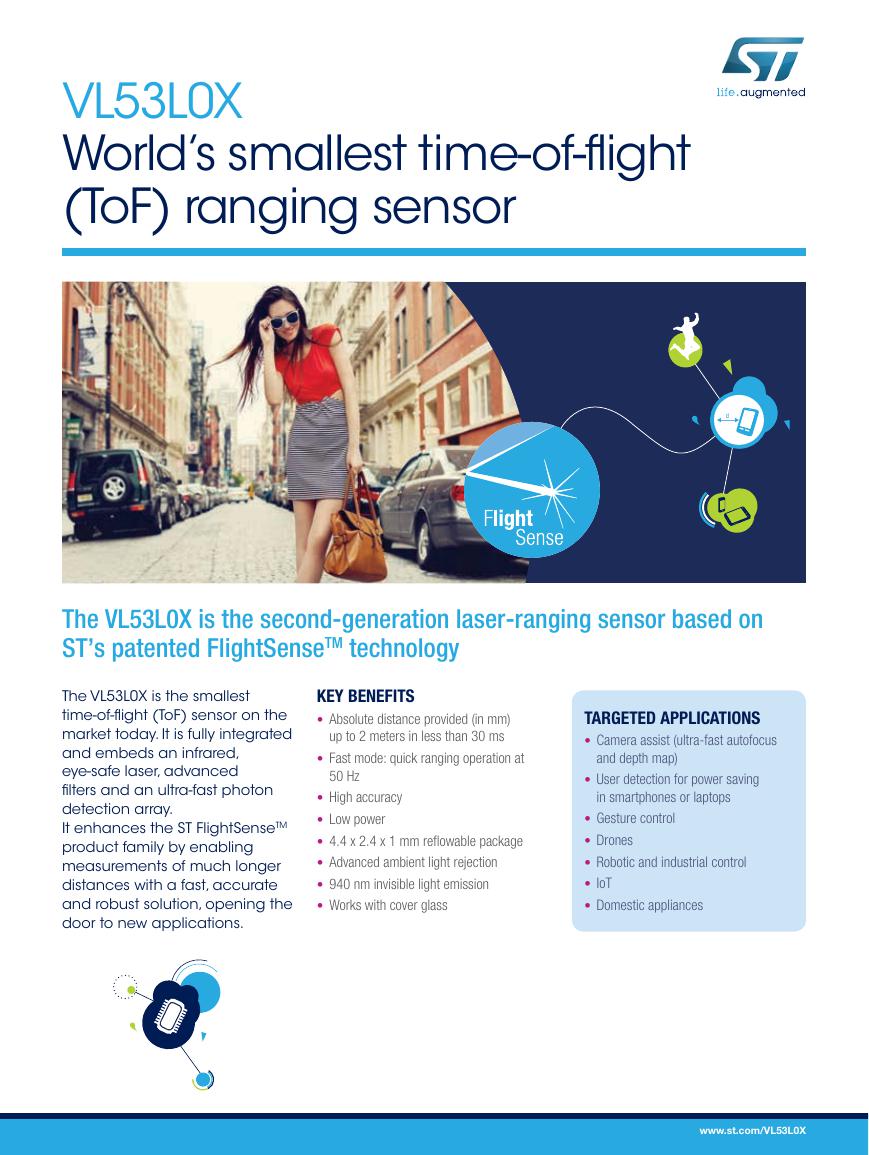 VL53L0X简要说明(En.FLVL53L00216).pdf
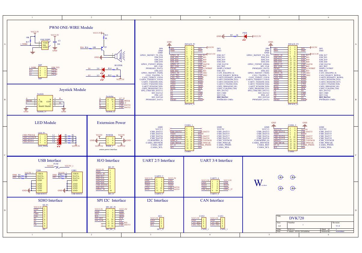 原理图(DVK720-Schematic).pdf
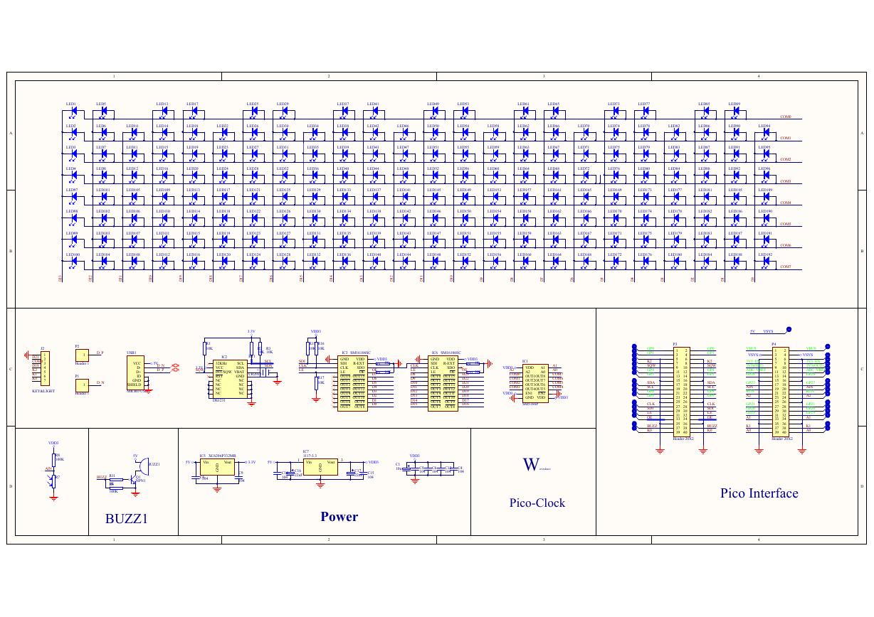 原理图(Pico-Clock-Green-Schdoc).pdf
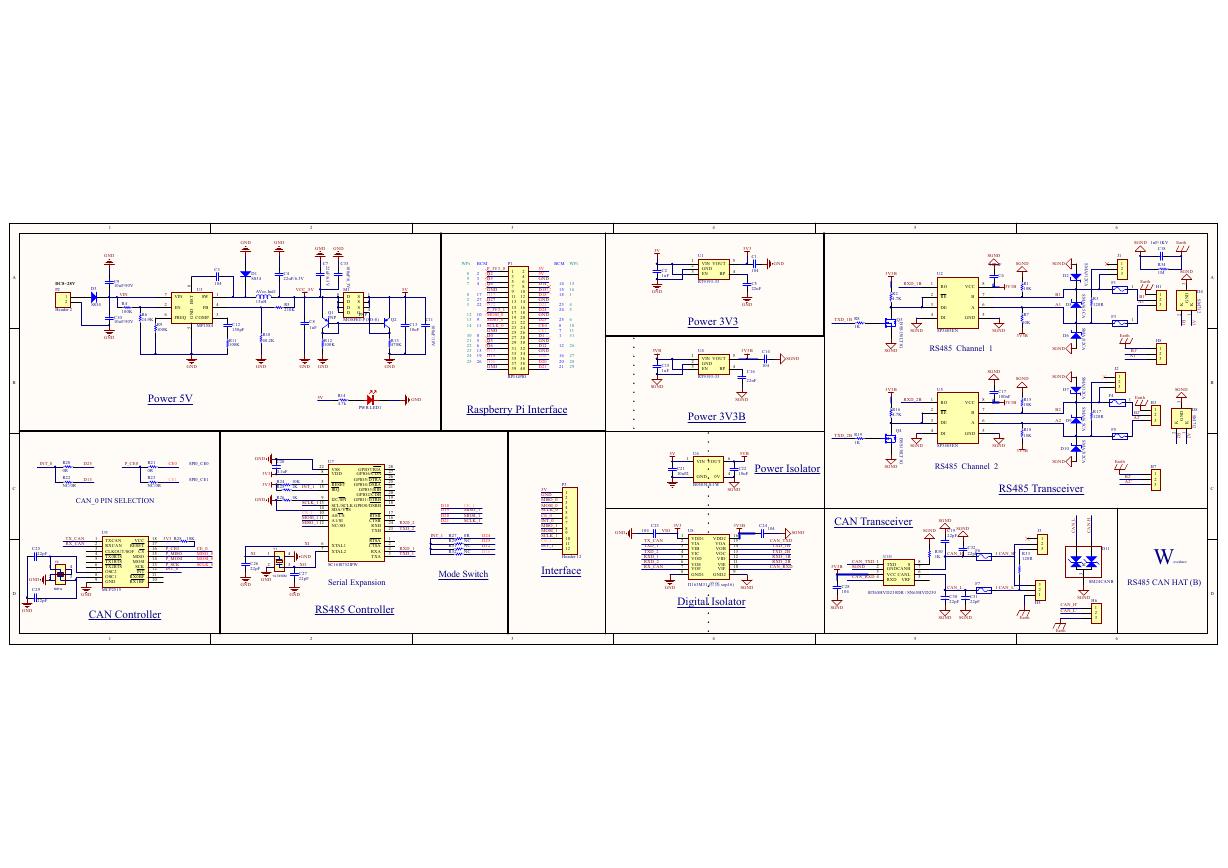 原理图(RS485-CAN-HAT-B-schematic).pdf
 File:SIM7500_SIM7600_SIM7800 Series_SSL_Application Note_V2.00.pdf
 ADS1263(Ads1262).pdf
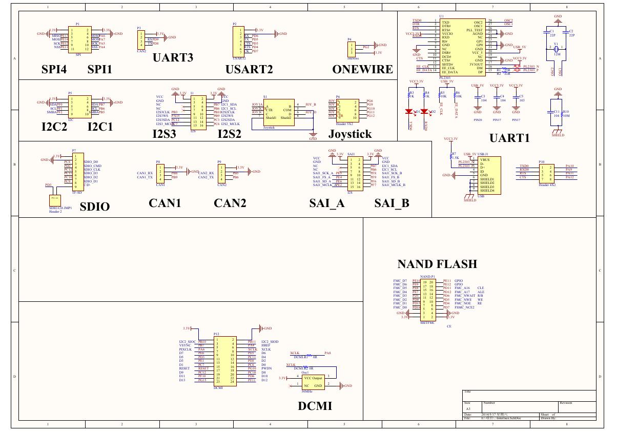 原理图(Open429Z-D-Schematic).pdf
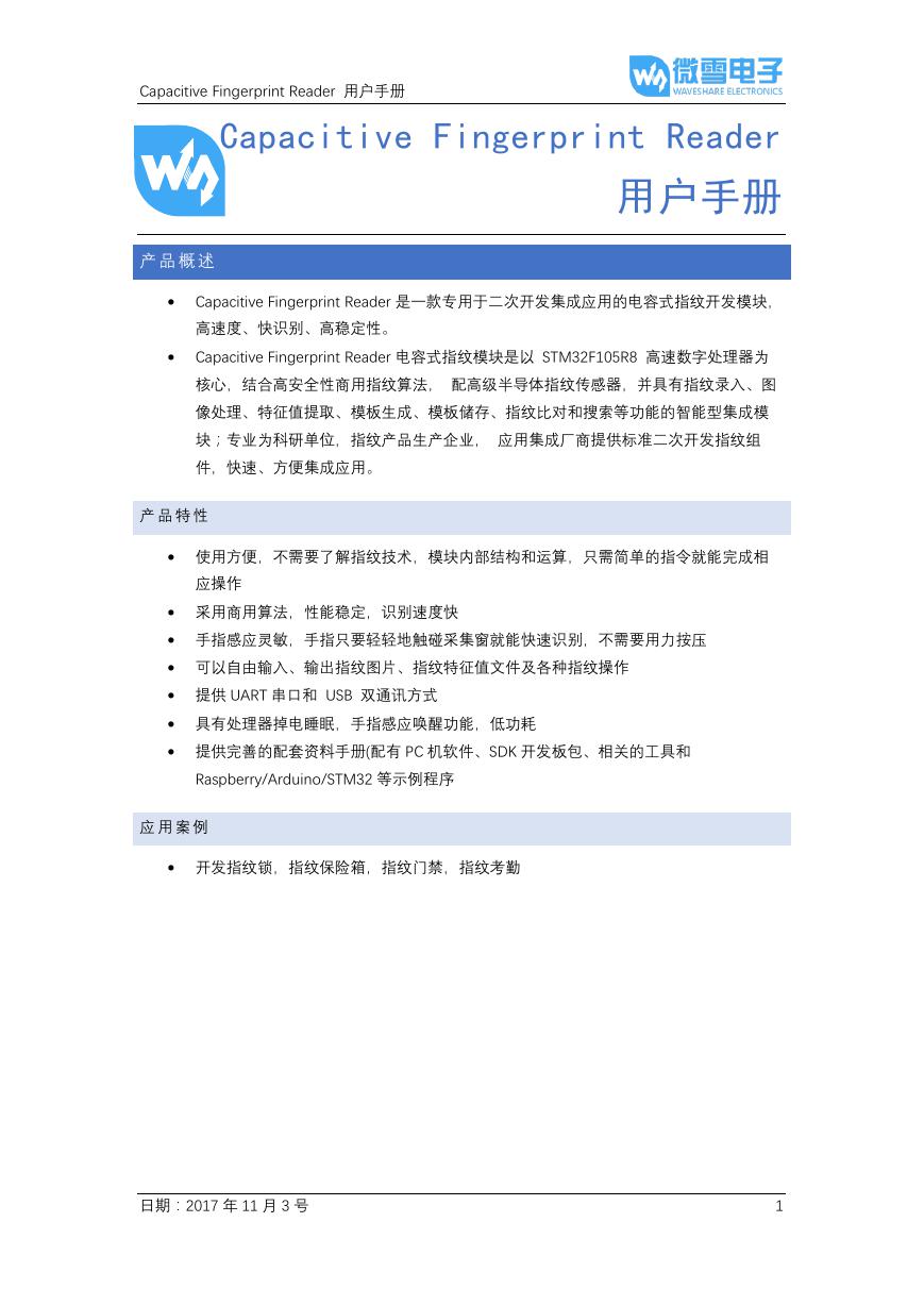 用户手册(Capacitive_Fingerprint_Reader_User_Manual_CN).pdf
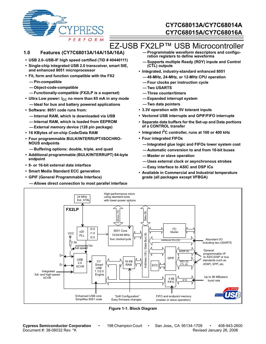 CY7C68013A(英文版)(CY7C68013A).pdf
 TechnicalReference_Dem.pdf